http://dx.doi.org/10.4236/epe.2014.62003
FPGA Implementation of Predictive Hysteresis Current
Control for Grid Connected VSI
Cristina Guzman, Kodjo Agbossou, Alben Cardenas
Hydrogen Research Institute and the Department of Electrical and Computer Engineering of Université du Québec à Trois-Rivières, Trois-Rivières, Canada
Email: [email protected], [email protected], [email protected]
Received October 1, 2013; revised November 1, 2013; accepted November 8, 2013
Copyright © 2014 Cristina Guzman et al. This is an open access article distributed under the Creative Commons Attribution License, which permits unrestricted use, distribution, and reproduction in any medium, provided the original work is properly cited. In accor-dance of the Creative Commons Attribution License all Copyrights © 2014 are reserved for SCIRP and the owner of the intellectual property Cristina Guzman et al. All Copyright © 2014 are guarded by law and by SCIRP as a guardian.
ABSTRACT
Grid connected voltage source inverters (VSIs) are essential for the integration of the distributed energy re-sources. Hysteresis current control (HCC) is a commonly employed method for power control of VSIs. This con-trol method, in contrast with voltage concon-trol, provides good dynamics, good stability and implicit over current protection. However, the most important concern of digital implementation of HCC is related with the sampling period of the measured currents. This paper presents a predictive hysteresis current control (HCC) for grid connected voltage source inverter and its FPGA implementation. Simulation and experimental results are pro-vided to verify the validity of the proposed implementation.
KEYWORDS
Distributed Generation (DG); Interconnected Power Systems; Hysteresis Current Control (HCC); Field Programmable Gate Array (FPGA)
1. Introduction
Modern power systems, looking forward to the Smart Grid concept, involve more and more the integration of the Distributed Energy Resources (DER) mainly based on clean energy sources like wind power (WP) and pho- tovoltaic (PV). The integration of these renewable re- sources to the utility grid becomes essential to improve the reliability and the capability of power systems. In this sense, the green house emissions can be greatly reduced. Voltage source inverters (VSIs) are power electronics circuits widely used to interface the DER with the utility power system.
In general, Grid connected VSIs are normally operated by controlling its output power, and, two possible control schemes can be implemented, either voltage or current control. For the voltage control, the phase angle and am-plitude of the output voltage are controlled according to the desired output power while on the current case; the current injected by the inverter is directly controlled to produce the desired output power. Hysteresis Current Control (HCC) was originally implemented as an analog
controller and it is often used for grid connected inverters configuration considering its fast transient response, good accuracy, implementation simplicity and inherently over-current protection [1-9].
Classic HCC has two main disadvantages, first the variable switching frequency depending on the load characteristics; and second, the degradation of its accu-racy when all digital implementations are required. Sev-eral modifications to the classic method have been intro-duced trying to overcome those problems [4-9]; most of the proposed methods seek for a constant switching fre-quency offering better performance than classic method. Most of the modified strategies of HCC offer better per-formances than the classic one when they are imple-mented using analog logic circuitry. However, when their implementation is made in digital processors like the field programmable gate arrays (FPGAs), without exter-nal aexter-nalog logic, the mean switching frequency is limited by the sampling rate of the analog-to-digital converters (ADCs).
con-trol taking into account the lately increase of FPGAs de-ployment in real-time measurement and control applica-tions. The HCC method introduced in this paper takes advantage of the real-time estimation of the utility volt-age by means of the hardware implemented VF-ADALINE with FLL [10,11]. The estimated signal of the utility voltage is employed to predict with high accuracy the output current of VSI within the sampling period of the measurement system with a higher sampling rate which is defined by the implemented structure of the VF- ADALINE.
The resulting oversampled signal of the VSI output current can then be used to implement, in an FPGA de-vice, the classic or modified HCC strategies with similar performances than the analog implementations.
Simulation and experimental results are presented showing a good accuracy of the all digital implementa-tion of HCC proposed. This predictive HCC has been validated by using a Xilinx FPGA as the digital target and a single phase grid connected VSI as the power elec-tronics application.
2. Hysteresis Current Control
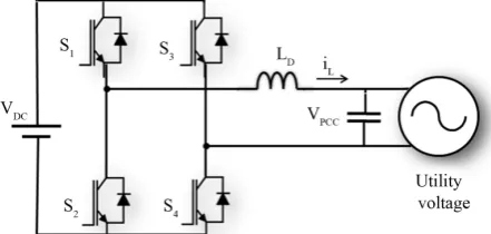
The Figure 1 shows a simplified circuit diagram of sin-gle phase grid connected VSI.
The filter inductor (LD) voltage can be written as func-tion of the output current using
d d L L D i V L t
= (1)
Then, the output current of the VSI can be computed if the inductor voltage (VL) information is available
1 0 1 d T L L D
i V t
L
=
∫
⋅ (2)1 0 0 T L L D V
i t I
L
= + (3)
In the case of grid-connected inverter, the inductor voltage depends on the voltage imposed by the controller (vDC(t)) and by the grid voltage (vPCC(t)). Using a full bridge single phase inverter with two conduction states
Figure 1. Simplified diagram of a single phase grid con-nected VSI.
(s1s4 and s2s3), the VDC can be defined by
( )
if 1 4if 2 3
DC DC
DC
V s s
v t
V s s
+ = −
(4)
The fundamental grid voltage will be
( )
sin( )
PCC PCC
v t =V ωt (5) where ω = 2 πf is the fundamental frequency of grid voltage
The inductor voltage when S1 and S4 are ON and S2
and S3 are OFF can be defined by
( )
sin( )
L DC PCC
v t =V −V ωt (6) If the S1S4 switching period is delimited by the 14
ON
T
and 14
OFF
T instants. The inductor current at the end of the switching period (at 14
OFF
T ) can be obtained by using
(
)
14( )
0 14 1 d OFF OFF T L L D T
i T v t t
L
=
∫
⋅ (7)(
)
(
)
(
)
(
)
14 14
14 0 0
0 cos cos OFF OFF OFF DC L D PCC T D V
i T T T
L V
T T i
L ω ω
ω
= −
+ − +
(8)
In the same way, if S2 and S3 are ON, the expression of the inductor current at the end of the switching period (at
23OFF
T ) can be written as
(
)
(
)
(
)
(
)
023 23 0
23 0 cos cos OFF OFF OFF DC L D PCC T D V
i T T T
L V
T T i
L ω ω
ω
= − −
+ − +
(9)
If all switches are OFF, the inductor current at the TR instant (TR> T0) can be defined as
( )
cos(
)
cos(
0)
0PCC
L R R T
V
i T T T i
L ω ω
ω
= − + (10)
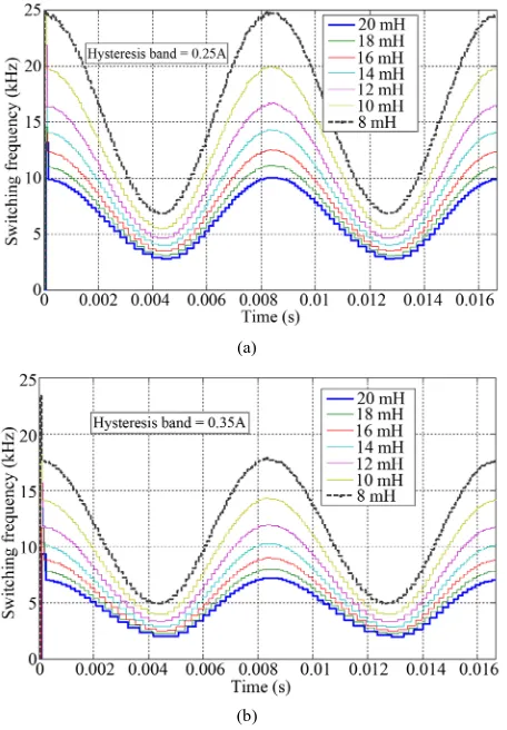
Considering an ideal sampling period (Ts 1 µs) the switching frequency depends on the grid and DC volt-ages, on the hysteresis band and on the filter inductor. Under this condition, the output current always remains within the hysteresis band (h).
Figure 2 shows the evolution of the instantaneous switching frequency during an electric period of 120 V/ 60 Hz grid voltage using different filter inductance (from 8 to 20 mH). The DC voltage is considered constant and set to 200 V. Figure 2(a)) shows the results for a hys-teresis band fixed to 0.25 A and Figure 2(b) is fixed to 0.35 A.
When the sampling period is around a few microsec-onds or tenths of microsecmicrosec-onds the current control error increases as the sampling period increases.
[image:2.595.308.540.130.380.2] [image:2.595.63.284.602.707.2](a)
[image:3.595.61.289.85.413.2](b)
Figure 2. Effect of the filter inductance on the instantaneous switching frequency during an electric period of 12 V/60 Hz grid voltage, a) hysteresis band = 0.25 A and b) hysteresis band = 0.35 A. DC voltage VDC = 200 V. Case of ideal
sam-pling period.
tracking error, during a half electric cycle (8.33 ms), considering different filter inductor and different sam-pling period. Here, the exceeding current tracking error is computed by using
( )
L( )
LREF( )
1CT
i k i k
e k
h
−
= − (11)
where iLREF is the desired current and h is the hysteresis band. eCT represents the exceeding error compared to the one obtained by using an ideal sampling period.
According to these results, the maximum current error can be very important when a low inductance (filter in-ductor) and a long sampling period are employed (TS> 10 µs) two or three times the hysteresis band. It is also to remark that even with a large inductor (see Figures 3(b) and (c)), an exceeding error greater than 0.5 p.u may ap-pears because the sampling and the ideal switching in-stants do not match.
3. Proposed Hysteresis Current Control
Taking into account that the main drawbacks of a digital
(a)
(b)
[image:3.595.310.539.85.578.2](c)
Figure 3. Effect of the filter inductance on the instantaneous current tracking error during a half electric period of 120 V/60 Hz grid voltage. Sampling period a) 5 µs b) 10 µs and b) 20 µs. DC voltage VDC = 200 V, hysteresis band = 0.25 A.
sam-pling rate imposed by the direct digital synthesis module VF-DDS (TDDS) which is higher than the one of the ADCs (TS). Figure 4 shows a simplified diagram of the VF-ADALINE with FLL as proposed in [11].
It is important to highlight that the estimation of the voltage signal is made by adjusting, online, the frequency of the VF-DDS, this feature warrants a very high accu-racy of the online utility voltage tracking.
The estimated signal of voltage (vPCC-E(k)) is then em-ployed to predict the output current of the inverter by using
( )
( )
(
)
( )
if
1 if
L M S
L E
L E DDS DDS
i k T
i k
i k m k T T
− −
−
↑
=
− + ⋅ ↑
(12)
where the –E subscript correspond to the estimated sig-nals and the–M ones to the measured sigsig-nals; ↑TS is the rising edge of the clock signal of the measurement sys-tem (ADC clock); ↑TDDS is the rising edge of the clock signal of the VF-ADALINE which is also employed as a clock signal for the current controller; and m(k) is the current slope which is defined by
( )
( )
( )
( )
( )
( )
14
23
if
if
Otherwise
DC PCC E D
DC PCC E D
PCC E D
v k v k
S L
v k v k
m k S
L
v k
L
−
−
−
−
− −
= −
(13)
where vDC(k) is the DC voltage of the inverter, and LD is the filter inductor which are known values. S14 and S23
signals correspond to the gating pulses ON state. As shown in Figure 5, the proposed current control scheme takes into account the effect of the dead time added to the gating signals and as illustrated, h is consid-ered as an input signal. The proposed control scheme can be used with fixed or with variable hysteresis band.
4. Hardware in the Loop Co-Simulation
[image:4.595.312.535.85.232.2]The Figures 4 and 5 schemes have been implemented for
Figure 4. Simplified diagram of VF-ADALINE with FLL for real-time signal estimation [11]. fVpcc-E: Estimated
[image:4.595.92.288.341.426.2]frequency.
Figure 5. Simplified diagram of of the proposed current control scheme.
the Xilinx Virtex-II-Pro (xc2vp30-7ff896) FPGA by us-ing System Generator and MATLAB/Simulink. Also a single phase grid connected VSI has been implemented in order to simulate the behavior of the proposed method and compare it to the classic method.
Further, some hardware-in-the-loop (HIL) co-simula- tions have been carried out as a preliminary validation of the proposed scheme. For these tests, the controller runs step-by-step in the FPGA and the model of the electric system (model of measurement, power electronics, utility source, etc.) runs on the MATLAB/Simulink. The main characteristics of the system are presented in Appendix.
Figure 6 shows a comparison, during 3 ms, of the co- simulation results of the classic HCC and the proposed predictive HCC. In this case, the filter inductance is LD = 12 mH, the voltage and current signals are sampled with
TS = 10 µs and the VF-ADALINE works at TDDS= 1 µs. It is evident the improvement of the current tracking with the predictive method which keeps the current tracking error inside the defined hysteresis band.
Several simulations have been carried out using dif-ferent filter inductances, and then the total harmonic dis-tortion (THD) of the VSI current has been computed for each case. The results are summarized in Table 1, show-ing the advantage of the proposed control scheme as the current THD is improved.
It is important to highlight that a large filter inductor permits a low current distortion (THD < 6%) using the classic HCC. IEEE standards recommend that the har-monic current injection at the point of common coupling of the distributed energy resources with utility must be under 5% [12]. On the other hand, it is well known that a large filter inductor limits the dynamics of VSI and the maximum output power of VSI [13].
5. Experimental Results
[image:4.595.66.284.582.698.2](a)
[image:5.595.60.287.82.364.2](b)
Figure 6. Comparison of the co-simulation results of the current tracking of grid connected VSI using a) classic HCC and b) predictive HCC. Utility voltage is 120 V/60 Hz, Sampling period TS = 10 µs, DC voltage VDC = 195 V, h = 0.3
[image:5.595.309.538.354.695.2]A.
Table 1. Total harmonic distortion of VSI output current when the hysteresis band is fixed to 0.3A and the output power is set to 500 W.
Filter Inductance (mH)
THD (%)
Classic HCC Proposed HCC
8 6.6 3.5
10 6.0 4.5
12 6.1 4.0
14 5.5 3.7
16 5.3 3.7
18 5.2 4.1
20 5.1 3.8
modified including the proposed current predictor and the VF-ADALINE with FLL [11]. Then, the resulting power control scheme has been implemented in a Xilinx xc2vp30-7ff896 FPGA device.
The power control scheme has been implemented con-sidering both the classic and the proposed hysteresis cur-rent controllers in order to compare them.
Several tests have been carried out using a single phase
grid connected VSI with the same characteristics used in simulation (see Appendix). The J-TAG link of the Xilinx development system has been employed (programmed) to send the information of the measured and the reference currents and the measured voltage to the MATLAB/ Simulink user interface as proposed in [10]. The output buffers have been programmed to send the information of each wave with a sampling period of 10 µs. Then, the results are post-processed to plot the corresponding fig-ures.
Figure 7 shows the comparison of the experimental results of current tracking by using the classic and the predictive HCC methods. In this tests, the nominal utility voltage is 120 V/60 Hz, the sampling period is TS = 10 µs, the DC link voltage is 195 V, the hysteresis band is fixed at h = 0.3 A, and the output power of the VSI is set to 500 W. One cycle of the measured utility voltage is plotted in Figure 8.
The trajectories when the classic method is employed are presented in Figures 7(a) and (b) shows the results with the predictive method.
(a)
(b)
[image:5.595.57.286.472.625.2]Figure 8. One cycle of the measured utility voltage.
It is evident that the current tracking is better achieved when the predictive method is employed, and as expected the classic HCC allows a higher error in the current tracking compared to the predictive method (zoomed zones of Figure 7(a)). This behavior is not suitable be-cause produces low frequency components in the output current which are difficult to filter and can also produce resonance if LC or LCL filters are employed.
Figure 9 shows the current waves obtained experi-mentally by means of a digital oscilloscope; Figure 9(a) shows the results with the classic HCC and Figure 9(b) the results with the predictive method. The spectrum of these current waves have been obtained and plotted in Figure 10. The two spectrum plots have been superposed in the same figure.
These experimental results confirm the expected and simulated behavior of predictive HCC; in fact the current spectrums show that the low frequency components are better attenuated with the predictive method. The spectral distribution, which is highly spread in the classic HCC, shows a dominant high frequency in the predictive method like in a constant switching frequency PWM.
It is important to remark that in the experimental tests carried out in this work, the DC link voltage has not been measured and it is supposed to be constant during the test. This assumption is done in order to compare the two control schemes in similar hardware conditions. It is then expected that better results could be obtained if the VDC
measure is introduced in the predictive HCC controller.
6. Conclusions
This paper proposes a new predictive hysteresis current control scheme for grid connected VSI and its hardware implementation using FPGA.
This new approach is based on the oversampled esti-mation of the utility voltage by means of the variable frequency ADALINE with frequency locked loop (VF- ADALINE & FLL) and the prediction of the VSI output current within a sampling period of the measured signal with a higher sampling rate. The predicted current is used
(a)
[image:6.595.61.290.85.225.2](b)
Figure 9. Comparison of current waves obtained experi-mentally by using a) classic and b) predictive HCC methods with fixed hysteresis band (h = 0.3 A). Measurement con-version ratio 5 A/V.
Figure 10. Comparison of current spectrum obtained ex-perimentally by using classic and predictive HCC methods with fixed hysteresis band (h = 0.3 A).
to generate the gating pulses of VSI instead of the meas-ured signal, which is employed as protection and to ad-just the predictor online.
[image:6.595.317.530.455.615.2]possi-bility of fixed or variable hysteresis band operation in order to control the mean switching frequency.
The proposed scheme has been validated by simulation and by experiments using a single phase grid connected VSI and Xilinx FPGA device for the control implemen-tation.
Acknowledgments
This work was supported by the LTE Hydro-Québec, the “Bureau de l’efficacité et de l’innovation énergétiques du Québec” and the Natural Sciences and Engineering Re-search Council of Canada. The authors wish to thank the Xilinx University Program for the hardware, software and technical support.
REFERENCES
[1] P. D. Ziogas, “The Delta Modulation Technique in Static PWM Inverters,” IEEE Transactions on Industry Appli-cations, Vol. IA-17, No. 2, 1981, pp. 199-204.
http://dx.doi.org/10.1109/TIA.1981.4503925
[2] D. M. Brod and D. W. Novotny, “Current Control of VSI- PWM Inverters,” IEEE Transactions on Industry Appli-cations, Vol. IA-21, No. 3, 1985, pp. 562-570.
http://dx.doi.org/10.1109/TIA.1985.349711
[3] M. A. Rahman, T. S. Radwan, A. M. Osheiba and A. E. Lashine, “Analysis of Current Controllers for Voltage- Source Inverter,” IEEE Transactions on Industrial Elec-tronics, Vol. 44, No. 4, 1997, pp. 477-485.
http://dx.doi.org/10.1109/41.605621
[4] W. Stefanutti and P. Mattavelli, “Fully Digital Hysteresis Modulation with Switching-Time Prediction,” IEEE Tran- sactions on Industry Applications, Vol. 42, No. 3, 2006, pp. 763-769.
http://dx.doi.org/10.1109/TIA.2006.873665
[5] Y. Xue, Y. Wu and H. Zhang, “An Adaptive Predictive Current-Controlled PWM Strategy for Single-Phase Grid- Connected Inverters,” 33rd Annual Conference of the IEEE Industrial Electronics Society, 2007. IECON 2007, Taipei, 5-8 November 2007, pp. 1548-1552.
http://dx.doi.org/10.1109/IECON.2007.4460333
[6] P. A. Dahono, “New Hysteresis Current Controller for
Single-Phase Full-Bridge Inverters,” IET Power Elec-tronics, Vol.2, No.5, 2009, pp. 585-594.
http://dx.doi.org/10.1049/iet-pel.2008.0143
[7] C. N.-M. Ho, V. S. P. Cheung and H. S.-H. Chung, “Con-stant Frequency Hysteresis Current Control of Grid-Con- nected VSI without Bandwidth Control,” IEEE Transac-tions on Power Electronics, Vol. 24, No. 11, 2009, pp. 2484-2495.
http://dx.doi.org/10.1109/TPEL.2009.2031804
[8] G. Xiao-yun, L. Hui-jin and C. Yu-sheng, “A Novel Cur-rent Control Method for Three-Phase APF Based on Switched Affine System Model and Quadratic Stability,” 2010 Asia-Pacific Power and Energy Engineering Con-ference (APPEEC), Chengdu, 28-31 March 2010, pp. 1-4. http://dx.doi.org/10.1109/APPEEC.2010.5448521
[9] M. A. Elsaharty, M. S. Hamad and H. A. Ashour, “Digital Hysteresis Current Control for Grid-Connected Convert-ers with LCL Filter,” 37th Annual Conference on IEEE Industrial Electronics Society IECON 2011, Melbourne, 7-10 November 2011, pp. 4685-4690.
http://dx.doi.org/10.1109/IECON.2011.6120083
[10] A. Cardenas, C. Guzman and K. Agbossou, “Develop-ment of a FPGA Based Real-Time Power Analysis and Control for Distributed Generation Interface,” IEEE Tran- sactions on Power Systems, Vol. 27, No. 3, 2012, pp. 1343-1353.
http://dx.doi.org/10.1109/TPWRS.2012.2186468
[11] A. Cardenas, C. Guzman and K. Agbossou, “Frequency Locked Loop for Grid-Connected VSI Synchronization and Power Analysis,” 2012 IEEE International Sympo-sium on Industrial Electronics (ISIE), 28-31 May 2012, Hanzhou, pp. 1386-1392.
http://dx.doi.org/10.1109/ISIE.2012.6237293
[12] 1547-IEEE Standard for Interconnecting Distributed Re-sources with Electric Power Systems, IEEE Standards; in Standards Coordinating Committee 21 on Fuel Cells, Pho- tovoltaics, Dispersed Generation, and Energy Storage, 28 July 2003.
[13] M. Ohshima and E. Masada, “The P,Q Controllable Do-main of a Single Phase PWM Converter to Preserve Si-nusoidal AC Current Waveform,” IEEE Transactions on Power Electronics, Vol. 15, No. 3, 2000, pp. 485-494. http://dx.doi.org/10.1109/63.844509
Appendix
1) Simulation and experimental setup parameters AC Power Source: 120 VAC/60 Hz.
Measurement system: Sampling period: TS = 10 μs,
Resolution = 12 bits FPGA system:
Main clock period: TFPGA =10 ns
Multipliers input/output resolution 18 bits/35 bits VF-ADALINE and FLL:
TDDS = 1 µs.
Learning factor = 0.1 Harmonics order = 32
ROM sine table length: 2P = 215 Fundamental frequency: f0 = 60 Hz
FLL gain = 3
FLL updating period = 10 µs 2) Power electronics converter Voltage Source Inverter:
16A, 600V IGBT full bridge (IRAMX16UP60A) Filter inductor and capacitor: LD = 12 mH, C0 = 2 µF.