N A N O E X P R E S S
Open Access
Optimization of the Surface Structure on
Black Silicon for Surface Passivation
Xiaojie Jia
1,2, Chunlan Zhou
1,2*and Wenjing Wang
1,2Abstract
Black silicon shows excellent anti-reflection and thus is extremely useful for photovoltaic applications. However, its high surface recombination velocity limits the efficiency of solar cells. In this paper, the effective minority carrier lifetime of black silicon is improved by optimizing metal-catalyzed chemical etching (MCCE) method, using an Al2O3thin film deposited by atomic layer deposition (ALD) as a passivation layer. Using the spray method to eliminate the impact on the rear side, single-side black silicon was obtained on n-type solar grade silicon wafers. Post-etch treatment with NH4OH/H2O2/H2O mixed solution not only smoothes the surface but also increases the effective minority lifetime from 161 μs of as-prepared wafer to 333 μs after cleaning. Moreover, adding illumination during the etching process results in an improvement in both the numerical value and the uniformity of the effective minority carrier lifetime.
Keywords: Black silicon, MCCE, Passivation, Illumination
Background
Black silicon (b-Si), also called nanostructured surface silicon, shows much lower light reflection losses than conventional random pyramids [1] and thus is an ex-tremely promising material for photovoltaic applications [2]. Up to now, there are three kinds of way to fabricate b-Si: laser texturing [3], reactive ion etching (RIE) [4], and metal-catalyzed chemical etching (MCCE) [5]. Among these, RIE and MCCE techniques have obtained high expectations. However, from the point of view of industry matching and cost-effectiveness, MCCE method is much more suitable for large-scale production, since the conventional texturing process is also based on wet chemical etching [6].
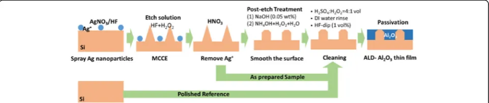
Ye et al. reported a novel nanoscale pseudo-pyramid texture formed by a MCCE technique and an additional NaOH solution treatment [7]: step 1, wafers were dipped into AgNO3/HF mixed solution to grow Ag nanoparti-cles on surface; step 2, wafers were steeped in the HF/
H2O2 mixed solution to do the MCCE process; step 3,
wafers were immersed in dense HNO3 to remove Ag
ions; and step 4, a NaOH solution treatment to reduce
the surface area and convert the microporous layer into a nanoscale pseudo-pyramid texture. This method has been proven as an efficient way to obtain high-efficiency black multi-crystalline (mc) silicon solar cells. Neverthe-less, there still is a room for optimization.
Firstly, etching process increases the surface recom-bination, so it is necessary that only the front side of the wafer is etched while the rear side gets protected. Nor-mally, the rear side can be protected by a mask before step 1 and the mask will be washed off after step 4 [8]. However, the preparation of the mask increases the process steps. Therefore, in our experiments, the spray method was used to deposit the AgNO3/HF mixed solu-tion onto the wafer surface. Since the spray method is applied to only one side of the sample, no preparation of the mask is necessary. Secondly, NaOH solution used in step 4 needs to be washed with HCl solution to remove Na+. If NH4OH/H2O2/H2O in the standard RCA cleaning is used, not only the alkaline treatment can be achieved but also the cleaning step can be omitted. Thirdly, in order to improve the reaction rate and the uniformity of the etching process, it is possible to refer to the photo-induced plating (LIP) technique by adding illumination during the etching process [9]. In the absence of illu-mination, because of the electrochemical potential of the oxidant (H2O2) being much more positive than
* Correspondence:[email protected]
1The Key Laboratory of Solar Thermal Energy and Photovoltaic System,
Institute of Electrical Engineering, Chinese Academy of Science (CAS), Beijing, China
2
University of Chinese Academy of Sciences (UCAS), Beijing, China
the valence band of Si, silver ions act as a catalyst to
rapidly reduce H2O2 and produce copious number of
holes injected into the valence band of Si [10]. If a certain amount of illumination is provided, the num-ber of photo-generated holes can be comparable with or higher than the holes obtained by reducing H2O2, thus accelerating the etching rate [8].
In order to improve the efficiency of solar cells, b-Si needs excellent surface passivation [11]. Although a wide variety of films can be selected, such as SiNx [12] and SiO2[13], the Al2O3thin film deposited by atomic layer deposition (ALD) is the best choice for passivating b-Si [14]. On the one hand, ALD, which has a conformal growth on surface with high aspect ratio features [15] and pinhole-free nature [16], is the natural choice for the coating of nanostructured surfaces. On the other hand, Al2O3is a suitable surface passivation material for silicon-based photovoltaic applications [17]. Al2O3 layer not only enables excellent chemical passivation due to strong coordination of Si and O [18] and selective hy-drogenation leading to a low interface state density after annealing [19], but also, it provides a strong field effect passivation through a high concentration of fixed negative charges [20] that leads to repulsion of charge carriers from the entire surface [21].
Methods
The experiments were performed on double-side polished n-type solar grade crystalline silicon wafers (COMTEC Co. Ltd.) of resistivity 1.7 ~ 13 Ω· cm. Single-side black silicon was fabricated using MCCE method. After spraying
the AgNO3/HF mixed solution (AgNO3in 0.001 mol/L,
HF in 0.24 mol/L) on the front side of wafer to de-posit silver nanoparticles, the wafers were rinsed by deionized (DI) water. Then, steep wafers into the
HF/H2O2 mixed solution for a few minutes to do
the MCCE process. According to different concen-tration ratio of HF and H2O2, the chemical etching solution is divided into two kinds: etch solution A,
HF (2.11 mol/L)/H2O2 (0.36 mol/L), and etch
solu-tion B, HF (0.42 mol/L)/H2O2 (0.18 mol/L). After
that, the wafers were immersed into concentrated
HNO3 solution for 10 min and then rinsed by DI
water to remove silver nanoparticles. In order to smooth the surface, alkaline solutions were used as post-etch treatment. Apart from the NaOH solution (0.05 wt%), NH4OH/H2O2/H2O mixed solution was also used, and the NH4OH content was adjusted
(NH4OH:H2O2:H2O = 0.2:1:5 (J), 0.5:1:5 (K), and
1.0:1:5 (L) (vol)). Schematics of the fabrication flow for the b-Si are shown in Fig. 1, using polished wafer as a reference.
After the post-etch treatments, samples were sequentially washed with H2SO4/H2O2mixed solution (H2SO4:H2O2= 4:1 vol) at 80 °C for 10 min, DI water rinse and HF-dip (1 vol%) at room temperature for 60 s. Al2O3thin film was deposited on both sides of wafers by plasma-enhanced atomic layer deposition (PE-ALD) at 200 °C. Trimethylalu-minium (TMA, Al2(CH3)6) was chosen as aluminum source and plasma oxygen as the oxidant. Polished samples (without b-Si) were also processed as references. The thick-ness of the thin film was about 10 nm, measured by ellipso-metry on polished wafers. The passivation was activated by post-annealing at the temperature of 450 °C for 10 min in ambient air.
In order to evaluate the anti-reflection quality of b-Si, the reflection spectrum was measured in the range of 300 to 1200 nm. The AM1.5G-weighted reflectance (RW) was calculated by Equation (1)
RW ¼
Z 1200
300 R
λ
ð ÞFPhð Þλ dλ Z 1200
300 F Phð Þλ dλ
ð1Þ
whereR(λ) is the measured reflectance andFPh(λ) is the
incident photon flux of the AM1.5G spectrum [22].
Ef-fective minority carrier lifetime maps of samples were measured after annealing using the microwave-detected
photoconductive decay (μ-PCD) (WT-2000, Semilab).
The surface morphology of b-Si was analyzed using high resolution scanning electron microscope (SEM) (Orion NanoFab, Zeiss), in which focused ion beam (FIB) was used to create the cross section.
[image:2.595.58.539.611.713.2]Results and Discussions
Effect of the Etch Solution
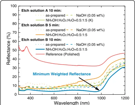
The reflectance spectrums of bare silicon etched by so-lutions A and B with different post-etch treatments are shown in Fig. 2 and the AM1.5G-weighted reflectance in Table 1, using polished wafer as a reference. Black sili-con achieves a reflectance below 10% in the whole visible spectrum as well as in the near UV and near IR regions. As a comparison, the reflectance of polished wafer without anti-reflection coating varies between 30 and 50% in the same wavelength range.
For as-prepared samples, the volume ratio of HF/ H2O2 in etch solutions A and B did not significantly affect the weighted reflectance at the same etching time. In etching for 10 min, samples show weighted reflectance of 8.4 and 8.6%, respectively, which are basically the same. Compared with the sample etched for less time, the value of the weighted reflectance decreases as the etching time increases.
However, samples etched by different solution shows dif-ferent performance after the post-etch treatment, taking samples with an etching time of 10 min as example. In post-etch treated by NaOH mixed solution, all samples show an increasing weighted reflectance, but samples etched by solution A increase more. In post-etch treated by NH4OH/H2O2/H2O mixed solution, sample etched by solution A still shows an increasing of weighted reflectance. However, the weighted reflectance of sample etched by so-lution B decreased after NH4OH/H2O2/H2O post-etching treatment and, finally, obtained the minimum value of weighted reflectance of 6%. This value is evidently better than the ones obtained in industrial alkaline-textured single crystalline silicon wafers or even the inverted pyramids of 15% without antireflection coating [23].
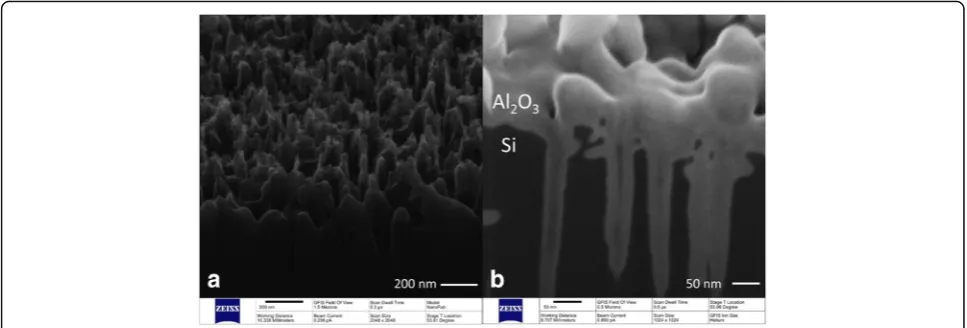
In order to improve the surface passivation of b-Si, a
10-nm Al2O3 thin film coating was deposited by
PE-ALD on both sides of wafers. Figure 3 shows the high resolution cross-sectional SEM picture of b-Si with and without Al2O3coating. Samples were etched by solution B and without any post-etch treatment after Ag+ re-moval. Compared with the samples without coating, a highly conformal Al2O3thin film can be observed on the entire surface of b-Si needles shown in Fig. 3b.
Figure 4 shows the effective minority lifetime for all
samples passivated by ALD-deposited Al2O3 thin film
and post-annealing. Annealing process affects a lot on the passivation quality of Al2O3thin film. The effective minority carrier lifetime of polished wafer was only 10 μs before annealing, and increased to 413 μs after. For the group of as-prepared samples, etching depth determines the values of the effective minority carrier lifetime. Sample etched by solution B for 5 min gives a relatively shallower etching depth and thus gains the highest value in this group. Post-etch treatment increases the effective minority carrier lifetime. For example, for samples etched by solution A for 10 min, the effective minority carrier lifetime was increased from 161μs before to 307 and 333μs after post-etch treatment of NaOH and NH4OH/H2O2/H2O, respectively. Regardless of the concentration of etching solution, the effective minority carrier lifetime is higher in NH4OH/H2O2/H2O post-etch-treated samples than in NaOH post-etch-post-etch-treated samples. Considering samples with high values of effective minority carrier lifetime were achieved through NH4OH/H2O2/ H2O post-etch treatment, NH4OH content in mixed solu-tion will be optimized.
Effect of the NH4OH Content in Post-etch Treatment An NH4OH/H2O2/H2O mixed solution having three different levels of volume ratio was used, in which NH4OH content was adjusted in 0.2:1:5, 0.5:1:5, and 1:1:5. During the preparation of these samples, the
Ag+ concentration in the AgNO3/HF mixed solution
was increased in order to strengthen the degree of
etching to further reduce the reflectance. The
weighted reflectance of as-prepared sample decreased
400 600 800 1000 1200
0 10 20 30 40 50 60 70 80 90 100
)
%(
e
c
n
at
c
elf
e
R
Wavelength (nm)
Etch solution A 10 min:
as-prepared NaOH (0.05 wt%)
NH4OH:H2O2:H2O=0.5:1:5 (K)
Etch solution B 5 min:
as-prepared NaOH (0.05 wt%)
NH4OH:H2O2:H2O=0.5:1:5
Etch solution B 10 min:
as-prepared NaOH (0.05 wt%)
NH4OH:H2O2:H2O=0.5:1:5
Reference (Polished)
Minimum Weighted Reflectance
[image:3.595.305.541.121.217.2]Fig. 2Reflectance spectrums of samples etched by solutions A and B with different post-etch treatments, using polished wafer as a reference
Table 1The AM1.5G-weighted reflectance of samples etched by solutions A and B with different post-etch treatments, using polished wafer as a reference
Weighted reflectance (%)
Post-etch treatment Etch solution
A 10 min B 5 min B 10 min
As-prepared 8.4 13.6 8.6
NaOH (0.05 wt%) 12.0 10.7 9.8
NH4OH:H2O2:H2O = 0.5:1:5 9.9 13.0 6.0
[image:3.595.56.291.509.692.2]from 8.4% of the original AgNO3/HF mixed solution to 6.8% of the new.
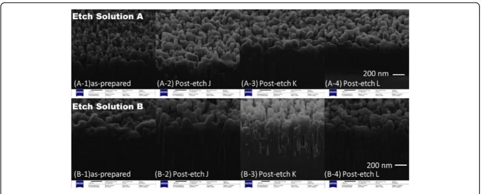
Figure 5 shows the SEM images of samples before and after post-etch treatment. The size of the nanostructure of samples etched by solution A for 10 min is 200 nm, while that of solution B is 500 nm. Post-etch treatment has a great influence on surface morphology. Without the post-etch treatment, the as-prepared samples have rough surfaces with many sharp burrs. After the post-etch treatment, samples’ surfaces become smooth and bright. And the size of the nanostructure is not obvi-ously changed through post-etch treatment. Neverthe-less, changing the NH4OH content in post-etch solution has no significant effect on surface morphology.
The reflectance spectrums of samples as well as the AM1.5G-weighted reflectance are shown in Fig. 6. Al-though the reflectance spectrum has some changes in
the shape of lines, the effect of NH4OH content on the anti-reflection quality of b-Si on solar cells is very small, because the AM1.5G-weighted reflectance is almost un-changed at different NH4OH contents.
However, a decrease of effective surface recombination velocity is observed as a function of the NH4OH content in mixed solution shown in Fig. 7. For black silicon sur-faces, the total recombination caused by nanostructure can be reduced to a flat plane just below the nano-structure using an effective surface recombination velocity [24]. And the value of the effective surface recombination velocity can be calculated from the measured effective minority carrier lifetime according to Equation (2):
1
τeff¼
1
τbþ
SfrontþSBack
W ð2Þ
whereτeffis the measured effective minority carrier lifetime,
τbis the carrier bulk lifetime,Wis the wafer thickness,Sfront
andSBackare the effective surface recombination velocity of
front surface and back surface, respectively. Assuming an
infinite carrier bulk lifetime [25], the effective surface
re-combination velocity can be calculated rather easily. The corresponding surface recombination velocity for polished
reference is Sfront=SBack=Seff= 22 cm/s. In the case of
black silicon, only the front surface has nanostructure, and
the back surface is polished. Equation (2) and infinite
car-rier bulk lifetime assumption are still valid, and the effective surface recombination velocity of back surface can be taken as the value of polished reference. Therefore, the sample that was etched by solution A and post-etch-treated by
NH4OH/H2O2/H2O (volume ratio 1.0:1:5) mixed solution
achieves the minimum effective surface recombination velocity of 38 cm/s. This value is smaller than the 56 cm/s
that Oh et al. [26] reported for their 18.2% efficient metal
etched b-Si solar cell.
Fig. 3The cross-sectional SEM picture of b-Si.aSamples etched by HF/H2O2mixed solution without Al2O3coating.bSamples etched by HF/ H2O2mixed solution with 10 nm Al2O3coating
0 50 100 150 200 250 300 350 400 450 500
Reference (Polished) NH4OH:H2O2:H2O
0.5:1:5 (vol) NaOH
(0.05 wt%)
e
mi
t
efi
l
r
ei
rr
a
c
yti
r
o
ni
M(
s
)
Post-etch Treatment
Etch solution A-10 min B-5 min B-10 min
Reference (Polished) With ALD-Al2O3 (10nm post-annealed)
as prepared
[image:4.595.56.540.88.252.2] [image:4.595.57.290.506.682.2]Post-etch treatment smoothes the surface, and increasing NH4OH content in mixed solution will enhance the smoothness. Technically, this process will usually lead to increased reflectance. But because of the deep structure of nanowires, the effect of increasing NH4OH content on the reflectance is not obvious. However, increasing NH4OH content can greatly improve the effective minority carrier lifetime. This means increasing the NH4OH content in mixed solution can improve the electrical properties of b-Si without sacrificing the optical properties.
Effect of the Illumination in Etching Process
In order to further improve the reaction rate of the etching process, bulb illumination was added on the basis of indoor
lighting during MCCE process in the HF/H2O2 mixed
[image:5.595.56.540.86.281.2]solution. According to the etching principle of MCCE method, the number of holes injected into the valence band of Si has a great influence on the etching rate. In indoor lighting conditions, because the intensity of illumination is low, so the etching rate depends on the concentration of silver ions acting as a catalyst and H2O2acting as an oxidant [8]. However, adding a bulb illumination on the basis of indoor lighting, because the intensity of illumination is high enough to obtain a sufficient number of minority carriers, so the etching rate is accelerated by photo-generated carriers.
Figure 8 compares the cross-sectional SEM images of samples etched for 5 and 10 min, respectively, under the Fig. 5SEM picture of samples etched by solutionsaandb(10 min) with different post-etch treatments
400 600 800 1000 1200
0 10 20 30 40 50 60 70 80 90 100
Weighted Reflectance (%) Post-Etch Treatment
NH4OH:H2O2:H2O
Etch solution A 10 min
Etch solution B 10 min
J 0.2:1:5 9.0 7.9
K 0.5:1:5 7.8 8.4
L 1.0:1:5 7.5 8.1
)
%(
e
c
n
at
c
elf
e
R
Wavelength (nm)
Etch solution A 10 min:
J: NH4OH:H2O2:H2O=0.2:1:5 K: NH4OH:H2O2:H2O=0.5:1:5 L: NH4OH:H2O2:H2O=1.0:1:5
Etch solution B 10 min:
J: NH4OH:H2O2:H2O=0.2:1:5 K: NH4OH:H2O2:H2O=0.5:1:5 L: NH4OH:H2O2:H2O=1.0:1:5
Fig. 6Reflectance of samples etched by solutions A and B with different post-etch treatments
[image:5.595.305.539.496.683.2] [image:5.595.58.290.523.702.2]conditions of indoor lighting illumination and bulb illu-mination. Samples were etched by solution B and with-out any post-etch treatment after Ag+ removal. In the absence of bulb illumination, comparing samples etched for 5 and 10 min in Fig. 8a, c, respectively, the etching depth is increased by extending the etching time. How-ever, when the etching time is 5 min, comparing samples etched without and with bulb illumination in Fig. 8a, b, respectively, the addition of bulb illumination does not increase the etching depth in the same etching time, but makes the nanostructure more compact and uniform. That is, illumination-enhanced wet chemical etching makes the size of nanostructures smaller and the surface of b-Si denser.
Being different with the effect on the surface morph-ology, adding bulb illumination during the etching process
has no obvious influence on samples’ reflectance, as shown in Fig. 9. The weighted reflectance of the three samples is about 7%, without obvious difference. However, the addition of bulb illumination can greatly improve the effective minority carrier lifetime, which increased from 188μs under indoor lighting illumination to 230μs under bulb illumination, as shown in Fig. 10. Moreover, the uni-formity of effective minority carrier lifetime on the whole surface was also improved a lot. This is consistent with the fact that the addition of bulb illumination makes the surface morphology more uniform. In a word, adding bulb illumination in etching process changes little on reflection but increases the effective minority carrier lifetime as well as the uniformity.
Fig. 8Cross-sectional SEM images of samples etched for 5 and 10 min, respectively, under the conditions of indoor lighting illumination and bulb illumination. Samples were etched by solution B and without any post-etch treatment after Ag+removal.aSample etched for 5 min under indoor lighting.bSample etched for 5 min under bulb illumination.cSample etched for 10 min under indoor lighting
400 600 800 1000 1200
0 5 10 15 20 25 30 35
Wavelength (nm)
Etch solution B as-prepared
10 min 5 min
5 min with Illumination
Reflectance (%)
[image:6.595.56.541.87.222.2]Fig. 9Reflectance of samples etched for 5 min and 10 min, respectively, under the conditions of indoor lighting illumination and bulb illumination. Samples were etched by solution B and without any post-etch treatment after Ag+ removal
[image:6.595.306.539.487.664.2] [image:6.595.57.291.502.682.2]Conclusions
Black silicon was fabricated on n-type solar grade silicon wafers using an optimized MCCE method and passivated using an ALD-deposited Al2O3 thin film, post-annealed. Spray method for the deposition of silver ions results in a single-side etching without using masks. After post-etch treatment, b-Si exhibits a low reflectance of 6–10%. The use of NH4OH/H2O2/H2O in place of NaOH as post-etch treatment to smooth the surface not only achieves higher effective minority carrier lifetime of 333μs but also elimi-nates the need for the Na+removal step. At the same time, increasing the NH4OH content in the post-etch solution can improve the effective minority carrier lifetime without significantly increasing the reflectance. Also, an effective surface recombination velocity of 38 cm/s is achieved on sample post-etch treated by NH4OH/H2O2/H2O (volume ratio 1.0:1:5) mixed solution, while the value of polished reference is 22 cm/s. Moreover, by adding illumination during the etching process, the etching rate can be increased, and a finer uniform surface can be obtained, resulting in an improvement in both the numerical value and the uniformity of the effective minority car-rier lifetime.
Acknowledgements
The project was supported by the National High Technology Research and Development Program of China (Grant No. 2015AA050302).
Authors’Contributions
XJ performed the sample characterization, analyzed the results, and wrote the manuscript. CZ carried out the sample preparation and helped in drafting the manuscript. WW participated in the discussion of experimental results and coordination. All authors read and approved the final manuscript.
Competing Interests
The authors declare that they have no competing interests.
Received: 28 November 2016 Accepted: 9 February 2017
References
1. Clapham PB, Hutley MC (1973) Reduction of lens reflexion by the“Moth Eye”Principle. Nature 244:281–282
2. Toor F, Branz HM, Page MR, Jones KM, Yuan H (2011) Multi-scale surface texture to improve blue response of nanoporous black silicon solar cells. Appl Phys Lett 99:103501
3. Her T, Finlay RJ, Wu C, Deliwala S, Mazur E (1998) Microstructuring of silicon with femtosecond laser pulses. Appl Phys Lett 73:1673–1675
4. Yoo J, Gwonjong YU, Junsin YI (2011) Large-area multicrystalline silicon solar cell fabrication using reactive ion etching (RIE). Sol Energy Mater Sol Cells 95:2–6 5. Koynov S, Brandt MS, Stutzmann M (2006) Black nonreflecting silicon
surfaces for solar cells. Appl Phys Lett 88:203107
6. Yue Z, Shen H, Jiang Y, Chen W, Tang Q, Jin J et al (2014) Large-scale black multi-crystalline silicon solar cell with conversion efficiency over 18%. Applied Physics A 116:683–688
7. Ye X, Zou S, Chen K, Li J, Huang J, Cao F et al (2014) 18.45%-efficient multi-crystalline silicon solar cells with novel nanoscale pseudo-pyramid texture. Adv Funct Mater 24:6708–6716
8. Huang Z, Geyer N, Werner P, De Boor J, Gosele U (2011) Metal-assisted chemical etching of silicon: a review. Adv Mater 23:285–308
9. Mette A, Schetter C, Wissen D, Lust S, Glunz SW, Willeke G et al (2006) Increasing the efficiency of screen-printed silicon solar cells by light-induced silver plating. Ieee, New York
10. Chattopadhyay S, Li X, Bohn PW (2002) In-plane control of morphology and tunable photoluminescence in porous silicon produced by metal-assisted electroless chemical etching. J Appl Phys 91:6134–6140
11. Zhong S, Huang Z, Lin X, Zeng Y, Ma Y, Shen W (2015) High-efficiency nanostructured silicon solar cells on a large scale realized through the suppression of recombination channels. Adv Mater 27:555–561 12. Jeong S, Garnett EC, Wang S, Yu Z, Fan S, Brongersma ML et al (2012)
Hybrid silicon nanocone–polymer solar cells. Nano Lett 12:2971–2976 13. Dou B, Jia R, Li H, Chen C, Meng Y, Liu X et al (2012) Research on the
surface passivation of nanostructure-textured crystalline silicon solar cell. Sci China-technological Sci 56:120–124
14. Otto M, Kroll M, Kasebier T, Ziegler J, Sprafke AN, Wehrspohn RB (2013) Passivation of optically black silicon by atomic layer deposited Al2O3. In: Brendel R, Aberle A, Cuevas A, Glunz S, Hahn G, Poortmans J et al (eds) Proceedings of the 3rd International Conference on crystalline silicon photovoltaics, vol 38. Elsevier Science Bv, Amsterdam, pp 862–865 15. Otto M, Kroll M, Kaesebier T, Tuennermann A, Salzer R (2012) Extremely low
surface recombination velocities in black silicon passivated by atomic layer deposition. Appl Phys Lett 100:191603
16. Van Hemmen JL, Heil SB, Klootwijk JH, Roozeboom F, Hodson C, De Sanden MC, Kessels WM (2007) Plasma and thermal ALD of Al2O3in a commercial 200 mm ALD reactor. J Electrochemical Soc 154(7)
17. Dingemans G, Seguin R, Engelhart P, De Sanden MCMV, Kessels WMM (2010) Silicon surface passivation by ultrathin Al2O3films synthesized by thermal and plasma atomic layer deposition. Physica Status Solidi-rapid Research Letters 4:10–12
18. Naumann V, Otto M, Wehrspohn RB, Hagendorf C (2012) Chemical and structural study of electrically passivating Al2O3/Si interfaces prepared by atomic layer deposition. J Vacuum Sci Technol 30(4)
19. Dingemans G, Beyer W, De Sanden MCMV, Kessels WMM (2010) Hydrogen induced passivation of Si interfaces by Al2O3films and SiO2/Al2O3stacks. Appl Phys Lett 97:152106
20. Hoex B, Gielis JJH, De Sanden MCMV, Kessels WMM (2008) On the c-Si surface passivation mechanism by the negative-charge-dielectric Al2O3. J Appl Phys 104:113703
21. Mallorqui AD, Alarconllado E, Mundet IC, Kiani A, Demaurex B, De Wolf S et al (2014) Field-effect passivation on silicon nanowire solar cells. Nano Res 8:673–681
22. Beneking C, Dauwe S, Zippel M, Zippel M (2004) Black Power® technology—a path towards higher efficiency in industrial silicon solar cell production, Presented at the 19th European Photovoltaic Solar Energy Conference and Exhibition
23. Chu AK, Wang JS, Tsai ZY, Lee CK (2009) A simple and cost-effective approach for fabricating pyramids on crystalline silicon wafers. Sol Energy Mater Sol Cells 93:1276–1280
24. Xiong K, Lu S, Jiang DS, Dong, Yang H (2010) Effective recombination velocity of textured surfaces. Appl Phys Lett 96:193107
25. Sproul AB (1994) Dimensionless solution of the equation describing the effect of surface recombination on carrier decay in semiconductors. J Appl Phys 76:2851–2854
26. Oh J, Yuan H, Branz HM (2012) An 18.2%-efficient black-silicon solar cell achieved through control of carrier recombination in nanostructures. Nat Nanotechnol 7:743–748
Submit your manuscript to a
journal and benefi t from:
7Convenient online submission 7Rigorous peer review
7Immediate publication on acceptance 7Open access: articles freely available online 7High visibility within the fi eld
7Retaining the copyright to your article