Temporal Evolution of Anodization Current of Porous
Silicon Samples
Adriana Gutiérrez1,2*, Jairo Giraldo1, Mario Enrique Rodríguez-García3
1Departamento de Física, Universidad Nacional de Colombia-Sede Bogotá, Ciudad Universitaria, Bogotá DC, Colombia; 2Depar- tamento de Física, Universidad Militar Nueva Granada, Bogotá DC, Colombia; 3Centro de Física Aplicada y Tecnología Avanzada, Universidad Nacional Autónoma de México, Querétaro, México.
Email: *[email protected]
Received June 15th, 2013; revised July 14th, 2013; accepted July 25th, 2013
Copyright © 2013 Adriana Gutiérrez et al. This is an open access article distributed under the Creative Commons Attribution License,
which permits unrestricted use, distribution, and reproduction in any medium, provided the original work is properly cited.
ABSTRACT
Temporal evolution of the anodization current of porous silicon samples was studied by means of a model of resistances connected in series that represented the temporal changes of the substrate and of the interface between the substrate and the electrolyte during the porous sample formation process. The porous samples were obtained by means of photoelec-trochemical etching of (100) n-type silicon wafers with different resistivity values, all in the range of 1 - 25 cm. The samples were formed at room temperature in an electrolytic bath composed by a mixture of hydrofluoric acid (48%) and ethanol having a composition ratio of 1:1 in volume under potentiostatic condition (10 V and 20 V) and an etching time of 2 minutes using back illumination provided by a laser beam with a wavelength of 808 nm.
Keywords: Porous Silicon; Electrochemical Etching; Anodization Current
1. Introduction
Porous silicon is a material formed by anodic dissolution of single crystalline silicon in hydrofluoric acid (HF) solu- tions [1]. Recent porous silicon applications include: de- velopment of optical biosensors [2], detection of organic solvents [3], detection of organic vapors (methanol, etha- nol, acetone and water) [4], among others.
The formation of porous silicon was first reported in the late 1950s as a result of electropolishing of silicon. Since then, particularly after 1990 when luminescence of porous silicon was discovered [5], extensive research had been undertaken [6-12]. Some of these investigations have re- vealed that porous silicon has many morphological fea- tures with properties that are very different from those of silicon. Also the formation process of porous silicon is very complex and it depends on many factors such as HF concentration, silicon type, current density, and illumina-tion intensity. However, these studies have not revealed the mystery of the morphology variations and their effect on the thermal and electrical properties of the composite system silicon/porous silicon (Si/PSi).
In this work, a theoretical model that allows to analyze the anodization current as a function of the etching time
of PS samples growth on (100) n-type silicon substrates with different resistivity values ( 1 - 25 cm) is pre- sented.
2. Experimental Setup
Porous silicon samples were obtained by using electro- chemical etching of (100) n-type silicon wafers with dif- ferent nominal resistivity values in the range (1 - 25 cm) (Mittel, Bromont-Ontario, Canada), see table 1 at room temperature in an electrolytic etching bath of 1:1 mixture of hydrofluoric acid (HF 48 wt%) and ethanol (96 wt%).
Most investigations related to porous silicon have been used galvanostatic anodization where the current intensity remains constant; however, the potentiostatic anodization which the anodization voltage is constant does not cause porous ramification during the growth process it assures the formation of the porous silicon with a more perfect and more uniform structure [13]. Furthermore, by means of potentiostatic anodization it is guaranteed that only one electrolytic process occur on the work electrode (silicon), but the reaction speed is generally small [14].
In this work the anodization was done potentiostatically with two voltage values (10 V and 20 V) and the etching time was 2 minutes under back illumination given by a
laser with wavelength of 808nm (LASERMATE GROUP INC. Model LBG 8080250 A5-T). Platinum slab of high purity was used as cathode [15]. Figure 1 is a diagram of the experimental setup used in the sample fabrication.
The current data were collected using a multimeter Keithley 2000 with a GPIB universal serial bus (USB) connected directly to a personal computer.
3. Experimental Results
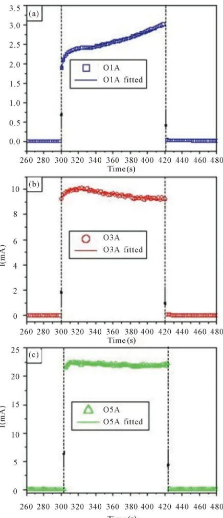
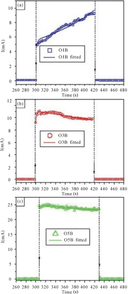
Figures 2 and 3 show the current as a function of etching time for different porous silicon samples that correspond to the wafers O1, O3 and O5. The samples O1A, O3A and O5A (see Figures 2(a)-(c)) were produced with the ano- dization O5voltage equal to 10V, while the samples O1B, O3B and O5B (see Figures 3(a)-(c)) with 20 V.
The current in all graphics of the Figures 2 and 3 shows two different behaviors with the etching time. The first occurs at approximately 20- 30 s and is related to the pore nucleation process. While the second corresponds to the remaining time and it is related to the porous growth process. These results concur to the stages of growth process as proposed by Kwon et al. [16] and Popkirov and Ottow [17]. In addition, it is observed that the current values increase when the substrate nominal resistivity is increased; this fact can be related with the electrochemical process that occurs in the interface between the substrate and the electrolytic solution.
4. Theoretical Model
When an n-type semiconductor is brought into contact with an electrolyte electrons will flow from the semi- conductor to the solution phase. The resulting excess charge in the solid semiconductor does not reside at the surface as it would in a metal, but instead is distributed in a region near the surface called the space charge region [18]. At large scale, the space charge just acts as a series interface resistance [19].
During the pores formation process the effective resis-tance of the substrate changes continuously because the region that is in contact with the electrolytic solution
[image:2.595.315.533.81.587.2]Figure 1. Diagram of the experimental setup.
Figure 2. Current as a function of etching time for three different porous silicon samples using an anodization volt- age of 10 V. (a) sample O1A ( 1 - 5 cm), (b) sample O3A ( 10 - 15 cm), (c) sample O5A ( 20 - 25 cm). The symbols represent the experimental data, whereas the continuous lines the best theoretical fit obtained by means of the Equation (3). : applied voltage on; : applied volt- age off. Dashed vertical lines were included to guide the eye.
[image:2.595.93.250.586.719.2]Figure 3. Current as a function of etching time for three different porous silicon samples using an anodization volt- age of 20 V. (a) sample O1B ( 1 - 5 cm), (b) sample O3B ( 10 - 15 cm), (c) sample O5B ( 20 - 25 cm). The symbols represent the experimental data, whereas the continuous lines the best theoretical fit obtained by means of the Equation (3). : applied voltage on; : applied volt- age off. Dashed vertical lines were included to guide the eye.
In this work the system formed by the substrate and the substrate/electrolyte interface was modeled by means of two resistances connected in series that change in the
time. The temporal variation of the effective resistance of the substrate is proposed as
s s
lm lp t R t
A t
(1)
where S and lm are the resistivity and the thickness of
each substrate (see Table 1), lp(t) is the pore depth and
A(t) is the the chemically active area of the pore tip. The expression (1) is similar to the one presented by Chri- stophersen et al. [22]. Due to the substrate thickness, lm,
is much greater than the pore depth, lp(t), this last one can
be rejected, i.e. lm-lp(t) lm. For A(t) an exponential
growth is proposed, t/S
o
A e , where S is a constant with
time dimensions.
The equivalent resistance of the interface between the substrate and the electrolyte has been modeled by means of a lineal variation with the time,
s el s el
R t R kt. (2)
In the Figures 2 and 3 the fitting of the experimental data have been included (continuous lines) modeling the current as
0
a
m
s t s s el
V I t
l
R k
A e
t
, (3)
with Va the anodization voltage. The obtained values for
the fitting parameters Ao, S, RS/el and k are registered in
Table 2.
[image:3.595.308.538.498.567.2]It is noteworthy that for the grown samples on the sub- strate with low resistivity value (wafer No. 1) the resis-
Table 1. Nominal resistivity and thickness values for the n-type silicon wafers.
Silicon wafer Nominal resistivity (cm)
Thickness lm
(m)
O1 1 - 5 523
O3 10 - 15 530
O5 20 - 25 502
Table 2. Value of the parameters Ao, S, RS/el and k ob- tained by means of the fitting of the current graphs as a function of the etching time.
Anodization voltage
Sample
name Ao (cm
2)
S(s) RS/el() K (/s)
O1A 610−5 2.16 4429.73 −9.13
Va = 10 V O3A 5.3410−3 5.67 979.69 0.97
O5A 5.2910−2 1.72 446.87 0.12
O1B 310−5 1.8 3641.73 −25
Va = 20 V O3B 1.4310−3 1.69 1796.96 2.37
[image:3.595.307.538.617.735.2]tance associated to the interface silicon/electrolyte di- minishes for the two anodization voltages used (see the negative values of the parameter k). In addition, the value of the parameter RS/el for Va = 20V is smaller than the
corresponding to Va = 10V, in contrast with the results
obtained for the other porous samples corresponding to the wafers O3 and O5. These effects maybe can be re- lated to the fact of having for the electrolyte a resistivity value (4 cm) greater than the corresponding value of the wafer (1 cm).
The resistivity of the hydrofluoric acid as a function of the concentration, for concentration values between 0 y 50 wt% 0˚C, is given by [23]
1
0.0104 %
HF cm
c
. (4)
Due to the concentration of the hydrofluoric acid used in the electrolytic solution for the growth of the porous samples studied in this work was of 24 wt%, the resistiv-ity of the electrolyte is obtained as 4 cm.
5. Conclusion
A simple theoretical model for the anodization current as a function of the etching time of porous silicon samples produced on n-type silicon substrates with different re- sistivity values was presented. The system formed by substrate and substrate/electrolyte interface was modeled through two resistances connected in series varying con- tinuously in the time during the anodization process. By means of the fitting of the experimental data of the current as a function of the time with the proposed model, it is obtained that the existence of a correlation is pro- bable between the resistivity values of the substrate and the resistivity of the electrolyte that does that the ef- fective resistance of the substrate/electrolyte interface diminishes for the grown samples on the substrates of smaller resistivity studied in this research.
6. Acknowledgements
This work was partially supported by COLCIENCIAS, Universidad Nacional de Colombia and UNAM. Adriana Gutierrez wishes to thank COLCIENCIAS (Colombia) (Programa de Créditos Condonables para Doctorados Nacionales 2004) and Dirección Nacional de Investigación DINAIN, Universidad Nacional de Colombia (Colombia) for their support.
REFERENCES
[1] X. G. Zhang, “Electrochemistry of Silicon and Its Ox-ides,” Kluwer Academic, Horwell, New York, 2001, p. 353.
[2] V. Torres-Costa, F. Agulló-Rueda,R. J. Martín-Palma and J. M. Martínez-Duart, “Porous Silicon Optical Devices
for Sensing Applications,” Optical Materials, Vol. 27, No.
5, 2005, pp. 1084-1087. doi:10.1016/j.optmat.2004.08.068
[3] M. Archer, M. Christophersen and P. M. Fauchet, “Elec- trical Porous Silicon Chemical Sensor for Detection of Organic Solvents,” Sensors and Actuators B, Vol. 106,
No. 1, 2005, pp. 347-357. doi:10.1016/j.snb.2004.08.016 [4] G. García Salgado, T. Díaz Becerril, H. Juárez Santie-
steban and E. Rosendo Andrés, “Porous Silicon Organic Vapor Sensor,” Optical Materials, Vol. 29, No. 1, 2006,
pp. 51-55. doi:10.1016/j.optmat.2006.03.012
[5] L. T. Canham, “Silicon Quantum Wire Array Fabrication by Electrochemical and Chemical Dissolution of Wafers,”
Applied Physics Letters, Vol. 57, No. 10, 1990, p. 1046.
doi:10.1063/1.103561
[6] V. Lehmann and H. Föll, “Formation Mechanism and Properties of Electrochemically Etched Trenches in n- Type Silicon,” Journal of the Electrochemical Society,
Vol. 137, No. 2, 1990, pp. 653-659. doi:10.1149/1.2086525
[7] R. L. Smith and S. D. Collins, “Porous Silicon Formation Mechanisms,” Journal of Applied Physics, Vol. 71, No. 8,
1992, pp. R1-R22. doi:10.1063/1.350839
[8] M. Ben-Chorin, F. Möller and F. Koch, “Nonlinear Elec- trical Transport in Porous Silicon,” Physical Review B,
Vol.49, No. 4, 1994, pp. 2981-2984. doi:10.1103/PhysRevB.49.2981
[9] O. Bisi, S. Ossicini and L. Pavesi, “Porous Silicon: A Quantum Sponge Structure for Silicon Based Optoelec- tronics,” Surface Science Reports,Vol. 38, No. 1-3, 2000,
pp. 1-126. doi:10.1016/S0167-5729(99)00012-6
[10] S. Lust and C. Levy-Clement, “Chemical Limitations of Macropore Formation on Medium-Doped p-Type Sili- con,” Journal of The Electrochemical Society, Vol. 149,
No. 6, 2002, pp. C338-C344. doi:10.1149/1.1475688 [11] X. Q. Bao, J. L. Lin, J. W. Jiao and Y. L. Wang, “Macro-
pore Density as a Function of HF-Concentration and Bias,”
Electrochimica Acta, Vol. 53, No. 2, 2007, pp. 823-828.
doi:10.1016/j.electacta.2007.07.065
[12] M. Balarin, O. Gamulin, M. Ivanda, M. Kosovic, D. Ris- tic, M. Ristic, S. Music, K. Furic, D. Krilov and J. Brnjas- Kraljevic, “Structural, Optical and Electrical Characteri- zation of Porous Silicon Prepared on Thin Silicon Epi- taxial Layer,” Journal of Molecular Structure, Vol. 924-
926, 2009, pp. 285-290.
doi:10.1016/j.molstruc.2008.10.045
[13] V. Parkhutik, J. M. Martínez-Duart, E. Elizalde Pérez Grueso, R. Díaz Calleja and E. Matveeva, “Método de Formación de Estructuras Luminiscentes de Silicio Po- roso,” Oficina Española de Patentes y Marcas, No. de Publicación: ES 2095793, España , 1997.
[14] J. I. Clavijo and E. Romero, “Efecto de Algunos Pará- metros Experimentales Sobre las Propiedades Ópticas y Morfológicas de Silicio Poroso Obtenido por Anodiza- ción de Silicio Tipo p,” Trabajo de Grado, Universidad Nacional de Colombia, Bogotá DC, 2004.
tial Photoacoustic Cell to Study in Situ the Growing Proc-
ess of Porous Materials,” Review of Scientific Instruments,
Vol. 81, No. 1, 2010, Article ID: 013901. doi:10.1063/1.3271238
[16] D. R. Kwon, S. Ghosh and C. Lee, “Growth and Nuclea- tion of Pores in n-Type Porous Silicon and Related Pho- toluminescence,” Materials Science and Engineering: B, Vol. 103, No. 1, 2003, p. 1-9.
doi:10.1016/S0921-5107(03)00126-0
[17] G. S. Popkirov and S. Ottow, “In Situ Impedance Spec-
troscopy of Silicon Electrodes during the First Stages of Porous Silicon Formation,” Journal of Electroanalytical Chemistry, Vol. 429, No. 1-2, 1997, pp. 47-54.
doi:10.1016/S0022-0728(97)00131-9
[18] X. G. Zhang, “Electrochemistry of Silicon and Its Oxides,” Kluwer Academic, Horwell, New York, 2001.
[19] J.-N. Chazalviel, F. Ozanam, N. Gabouze, S. Fella and R. B. Wehrspohn, “Quantitative Analysis of the Morphology of Macropores on Low-Doped p-Si,” Journal of the Elec- trochemical Society, Vol. 149, No. 10, 2002, pp. C511-
C520. doi:10.1149/1.1507594
[20] G. Barillaro, P. Bruschi and F. Pieri, “Two-Dimensional Macroscopical Simulations of Porous Silicon Growth,”
Computational Materials Science, Vol. 24, 2002, p. 99. [21] M. Ray, S. Ganguly, M. Das, S. M., Hossain and N. R.
Bandyopadhyay, “Genetic Algorithm Based Search of Pa- rameters for Fabrication of Uniform Porous Silicon Na- nostructure,” Computational Materials Science, Vol. 45,
No. 1, 2009, pp. 60-64.
dx.doi.org/10.1016/j.commatsci.2008.03.052
[22] M. Christophersen, S. Langa, J. Carstensen, I. M. Tigin- yanu and H. Föll, “A Comparison of Pores in Silicon and Pores in III-V Compound Materials,” Physica Status So- lidi (a), Vol. 197, No. 1, 2003, pp. 197-203.
doi:10.1002/pssa.200306499
[23] V. Lehmann, “Electrochemistry of Silicon: Instrumenta- tion, Science, Materials and Applications,” Wiley-VCH Verlag GmbH, Weinheim, 2002, p. 115.