International Journal of Emerging Technology and Advanced Engineering
Website: www.ijetae.com (ISSN 2250-2459, ISO 9001:2008 Certified Journal, Volume 7, Issue 4, April 2017)
158
Design of Hexagonal Shaped Microstrip Patch Antenna with
Metamaterial for mm Wave Application
L. Chandiea
1, K. Anusudha
2 1M.Tech, II year student, 2Assistant Professor, Dept. of Electronics Engg., Pondicherry University, Pondicherry, India.
Abstract- The current scenario in today’s wireless applications demands designing of antennas that are compact, robust and uncomplicated to integrate with RF circuit components. Microstrip patch antenna is one such kind which pleases these requirements. The two main performance parameters of an antenna, the gain and the bandwidth being near to the ground for patch antennas is the major drawback. Nominally, the gain range of a patch antenna is 1-2dB. The most candid tactic of aggregating these factors encompasses the use of low dielectric substrate with increased thickness, but this unavoidably leads to generation of surface waves. Consequently, sensible substrate thickness has to be employed. In this paper hexagon shaped patch antenna with metamaterial on the substrate for millimeter wave application is proposed. The analysis is done using Ansoft HFSS software version 15.0. The performance parameters analyzed are bandwidth, gain and return loss.
Keywords: Microstrip antenna; Hexagonal Shape; Metamaterial; Millimeter wave application.
I. INTRODUCTION
Microstrip patch antenna is one amongst widely apprehended antenna types in today’s scenario. Habitually microstrip antenna is as well signposted as patch or microstrip patch antenna. Microstrip antenna finds major application in the microwave frequency range for their compatibility, minimalism and ease of integration, shaping them cool to fabricate either as individual element or as arrays. The theory of the patch antenna was projected in 1953 by Deschamps. On the other hand, real-world antennas were industrialized in the 1970s by Munson and Howell. The exclusive asset of the patch antenna is its Two-Dimensionality. The simplest form of patch antenna entails a ground plane on one side of the substrate and a radiating patch on another side. The feed lines and the radiating elements are commonly photo etched on the substrate. Thus, it possesses precise low contour and printed circuit (photolithographic) technology can be used for fabrication process [1]. There are abundant patterns that can be used as feed to microstrip antennas like co-axial feed, line feed, aperture coupling, proximity coupling etc. Two analysing techniques are primarily employed for any patch antenna. They are namely the cavity model and transmission line model [2]. Microstrip arrays stay inadequate in that they have a tendency to radiate powerfully over a constricted frequency band and are not able to function at higher power levels used in coaxial line, waveguide [3].
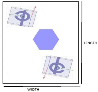
Engineers and scientists have been working for a long time studying other portions of the spectrum that can be used to develop wireless technologies. Millimeter Wave Wireless Technology or also known as (MMWT) presents the potential to offer bandwidth delivery comparable to that of fiber optics, but without the financial and logistic trials of deploying fiber. Millimeter wave generally corresponds to the radio spectrum between 30 GHz to 300 GHz, with wavelength between one and ten millimeters. The Federal Communications Commission (FCC) has allocated four frequency bands: 57 - 64 GHz, 71 -76 GHz, 81 - 86 GHz and 92 - 95 GHz for millimetre Wave Technology. Figure 1 shows a general layout of the proposed microstrip antenna
[image:1.595.358.524.391.546.2]
Figure 1. General layout of proposed antenna
International Journal of Emerging Technology and Advanced Engineering
Website: www.ijetae.com (ISSN 2250-2459, ISO 9001:2008 Certified Journal, Volume 7, Issue 4, April 2017)
159
Major advances in millimetre wave antennas have been made in recent years due to the high competition of users for the bandwidth and for the speed. In the previous work in order to achieve that characteristic, some techniques like cross slots [4], sorting pins, increasing the thickness of the patch [5], use of circular and triangular patches with proper slits [6] and antenna arrays were proposed. But these methods have their own demerits like complexity in design and degrading some effectiveness of the parameters of the antenna. In order to achieve multiband characteristics with higher gain that can be employed for MMW applications, in this work it is proposed to introduce metamaterial on the substrate.
Though relatively new in the world of wireless communication, the history of millimeter wave technology goes back to the 1890‟s when J.C. Bose was experimenting with millimeter wave signals at just about the time when his contemporaries like Marconi were inventing radio communications. Following Bose‟s research, millimeter wave technology remained within the confines of university and government laboratories for almost half a century. The technology started so see its early applications in Radio Astronomy in the 1960‟s, followed by applications in the military in the 70‟s. In the 80‟s, the development of millimetre wave integrated circuits created opportunities for mass manufacturing of millimeter wave products for commercial applications [16].
D. Sanchez-Hernandez and I. Robertson [21]
presented a 60 GHz active patch antenna using a Gunn diode as an oscillator in a reflection amplifier module where the patch acts as the resonant and radiating element as well as the stabilizing component for the oscillator. The tuning bandwidth obtained by varying the DC bias voltage is 62.277 GHz to 63.316 GHz and it is equivalent to a 1.6 % (1.039 GHz) bandwidth. Amar Adane, François Gallé and Christian Person [22] proposed an antenna built on a silicon membrane with an upper BCB (Benzo Cyclo-Buten dielectric material) thin film deposited and excited with U-shape and T-shape microstrip feeder via a dielectric gap which achieved a bandwidth of 13.3 %. A 60 GHz coplanar waveguide (CPW) fed patch antenna A Wideband Microstrip Patch Antenna for 60 GHz Wireless Applications implemented on a high dielectric constant substrate (εr = 9.9, which is close to the dielectric constant of commercial GaAs and CMOS process) was proposed by K. Hettak, G.Y. Delisle, G.A. Morin, S. Toutain and M. Stubbs [23]. This antenna covers from 58.3 GHz to 63 GHz. The hybrid dielectric resonator antenna proposed by Y. Coulibaly, M. Nedil, L. Talbi, T. A. Denidni [24] achieved 14.36 % bandwidth using stacking and superstrate schemes and aperture coupled feeding.
In [25] Duixian Liu, Johannes Akkermans and Brian Floyd proposed a balanced-fed aperture-coupled patch antenna with an air cavity embedded in the PCB stack which has about 7 dBi gain, with at least 12 GHz impedance bandwidth.
Sumanpreet Kaur Sidhu and Jagtar Singh Sivia [7] compared different shapes of patch antenna. From the results it can be inferred that pentagon shape gives higher gain and bandwidth compared to other shapes. A pentagon shaped microstrip patch antenna has been already developed for multiband application [27]. Hence
in this work the 2nd higher resulted hexagon shape has
been used.
Newly, the interest about metamaterial is increasing rapidly. Metamaterials (MTM) are unreal materials that are technically developed to have properties unavailable in nature. In 1967, Victor Georgievich Veselago [17] premeditated about electrodynamics of materials which
has simultaneous negative dielectric permittivity (ε) and
magnetic permeability (μ). As a result of negative ε and μ
metamaterials are known as Double Negative (DNG) materials and are also mentioned as Negative Index Materials due to its negative refractive index.
Metamaterial structure is composed of Split Ring Resonators (SRR) and thin wire elements that generate
negative μ and ε respectively. This structure is named as
resonator because it possessess magnetic resonance at some frequencies. The SRR comprises of two splitted metallic rings with the splits present on opposite sides. It acts as an LC resonator having high quality factor with distributed capacitance and inductance. Primarily four types of metamaterial structures can be used in substrate:
1-D Split Ring structure
Symmetrical Ring structure
Circular Split Ring structure
S structure
Metamaterial structure employed in patch antenna improves its performance parameters by enhancing the electric fields of EM waves propagating in free space. A circular waveguide array antenna with higher gain using metamaterial was proposed in [8]. In comparison with other three metamaterial structures, the Circular Spilt-Ring structure shows better directional beam and is easier to tune its permeability. Hence the proposed antenna makes use of this structure for improving the radiation.
II. WORKING PRINCIPLE
International Journal of Emerging Technology and Advanced Engineering
Website: www.ijetae.com (ISSN 2250-2459, ISO 9001:2008 Certified Journal, Volume 7, Issue 4, April 2017)
160
The field sign on the sides of patch incessantly changes with respect to the instantaneous phase of the applied signal. The electric fields spread out to the boundary of the patch, which are acknowledged as fringing fields, makes the patch to radiate. TM10 mode is the fundamental mode in a rectangle shaped patch. The resonant frequency of a patch antenna is influenced by size of ground plane, patch (impedance) width, metal
(copper) thickness and dielectric constant. The
advantages of patch antenna makes them fit for innumerable solicitations like vehicle based satellite link
[10], radar for missiles and mobile handheld
communication devices or radios, global positioning systems (GPS) [11], telemetry etc,. M. Abbaspour and H. R. Hassani [12] defined a star shaped patch for broadband application.
Incorporating a peculiar structure (metamaterial) on the conductor, makes it is possible to alter the
radiofrequency characteristics. A Smooth-textured
conducting plane (ground plane) possesslow surface impedance, while with addition of peculiar structure it has high surface impedance. This high-impedance surface reflects all the power as in-phase, instead of out-of-phase, allowing to place the radiating element straightaway close to the surface. Put differently, the image current direction is constructive, rather than destructive, permitting the antenna to radiate with increased efficiency.
III. PROPOSED ANTENNA DESIGN
Designing of the hexagon shaped microstrip antenna is
done with HFSS version 15.0 softare. ANSOFT HFSS
software is an industry standard for simulating 3-D, full-wave, electromagnetic fields. Its gold-standard accuracy, advanced solvers and high-performance computing technologies make it an essential tool for engineers tasked with executing accurate and rapid design in high-frequency and high-speed electronic devices and platforms. HFSS offers state-of the-art solver technologies based on finite element, integral equation, asymptotic and advanced hybrid methods to solve a wide range of microwave, RF and high-speed digital applications.
The problem faced in designing a hexagon shaped microstrip patch or any of its derivatives is that there are no available design formulations like other geometric shapes. This is because most of the work has been limited to the rectangular and circular patches. One way of overcoming this is to design by equating surface areas of the desired patch with that of a rectangular patch. This method was employed to obtain the radius of a circular microstrip patch. One reason for this method of equating areas is that the flux through equal surface areas would be equal.
A. Calculating antenna dimension
Formulation would be based on equating the areas of the hexagon patch with that of the rectangular patch. This is the rectangular patch model. The approximate width of the equivalent rectangular patch was calculated by using the
√
⁄ (1)
Where c- velocity of light f- Operating frequency
- Substrate’s relative permittivity
The operating frequency can be obtained by solving the below equation
√
⁄
Where c- velocity of light f- Operating frequency
- Substrate’s relative permittivity h- Thickness of the substrate.
The half of the width of rectangular patch was equated
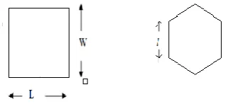
[image:3.595.349.510.448.525.2]to the desired hexagonal patch width l.
Figure 2 Rectangular and hexagonal patch Antenna
Rogers RT/duroid 5880 is used as the substrate for the proposed antenna. Its dielectric constant is 2.2. The patch width is taken as 14.14 mm and the thickness of the substrate is found to be 3mm. The length and breadth of the substrate is taken as 50*50 mm. The area of proposed
design is (50*50=2500 mm2).
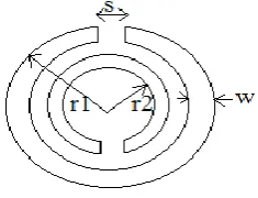
As stated before, the Circular Split Ring metamaterial structure was used for antenna design. Figure 3 shows the structure of a Circular Split Ring metamaterial simulated in HFSS. Its dimensions are determined using the following equations.
L1= (2 ) – S (3)
L2= (2 ) – S (4)
⁄
International Journal of Emerging Technology and Advanced Engineering
Website: www.ijetae.com (ISSN 2250-2459, ISO 9001:2008 Certified Journal, Volume 7, Issue 4, April 2017)
161
Where c- velocity of light
permittivity of the substrate.
f1- lower cut off frequency
f2- upper cut off frequency
[image:4.595.112.230.303.393.2]Same Roger RT/Duroid 5880 substrate is employed for metamaterial also. The dimension of Circular Split Ring on solving its equations is as follows: the radius of outer ring and inner ring are 0.1 and 0.05 mm respectively. The split gap and width are 0.1mm. The wire length, width are 1mm and 0.1mm respectively.
Figure 3 Circular Split Ring structure
[image:4.595.338.553.390.532.2]A partial ground plane was used to observe its effects on the impedance bandwidth of the hexagonal patch antenna when simulation was done. The dimension of the partial ground plane is 50 * 15 mm. No part of the ground plane is overlapped with the patch. This was done to avoid electromagnetic flux interference. The purpose of the ground plane is to overcome the spurious radiation of the particularly long microstrip transmission line in order to concentrate the radiation of the E and H fields onto the patch. This is believed to be able to improve the bandwidth of the patch. Figure 4 shows the layout designed in HFSS after adding metamaterial on the substrate. The total number of metamaterials added is limited to two. The position of the metamaterials is chosen by trial and error method to obtain the maximum gain.
Figure 4 Proposed antenna layout simulated in HFSS
IV. SIMULATION RESULTS
[image:4.595.58.271.611.748.2]The performance parameters such as gain, bandwidth and return loss of the proposed antenna are discussed in this section. The return loss conveys the mismatch. It can be described as, logarithmic ratio of the power reflected by an antenna to the power served from the transmission line to the antenna. The bandwidth states the frequency range over which the antenna can function acceptably. The bandwidth also defines the frequencies where the antenna exhibits an SWR less than 2:1. The radiation pattern designates the absolute power of the field radiated in various directions, at a constant distance from the antenna. Gain of an antenna is specified in reference to a standard antenna. The frequently used reference antennas are the isotropic antenna and the resonant half-wave dipole antenna. The process of computing gain of an antenna by relating it against a standard antenna, which has a standardized gain, is technically referred as gain transfer technique. The results obtained after adding metamaterial is tabulated in table 1.
Table 1.
Results obtained for the proposeddesign
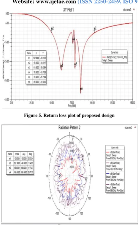
As indicated in Figure 5, the impedance bandwidth of proposed antenna with metamaterial and partial ground covers all the four mm wave bands defined by FCC. It has resonant frequencies at 61.6, 78.6 and 85.6 GHz. From the radiation profile shown in figure 6 it can be inferred that the gain is positive for all the resonant frequencies identified from the return loss pattern. The minimum gain is 3.92 dB and the maximum gain of 25.24 dB occurs at 85.6 GHz shown in Figure 6.
PARAMETER RESULTS
Resonant Frequency(GHz)
85.6
Return Loss(dB)
-41.65
Gain(dB)
25.24
No of mm Wave Band
International Journal of Emerging Technology and Advanced Engineering
Website: www.ijetae.com (ISSN 2250-2459, ISO 9001:2008 Certified Journal, Volume 7, Issue 4, April 2017)
[image:5.595.47.280.121.501.2]162
Figure 5. Return loss plot of proposed design
Figure 6 Radiation pattern for proposed design
V. CONCLUSION
As stated before antennas need to be specifically designed and optimized for the Millimeter Wave Technology (MMWT). At 60 GHz, the rain attenuation is high, and the electromagnetic losses are significant. More importantly, at this exact frequency there is a peak in oxygen absorption. Therefore higher gain wideband antenna is required for MMWT. The gain bandwidth product is a constant, therefore an effort has been made to improve the bandwidth of the patch antenna to use it for mm wave application by adding metamaterial, while ensuring desired radiation pattern. Further, the effects of surface waves and mutual coupling are also minimized by the use of metamaterial. In conclusion, the hexagonal patch antenna with metamaterial on the substrate is capable of operating in all the four mm wave frequency bands of 57 - 64 GHz, 71 -76 GHz, 81 - 86 GHz and 92 - 95 GHz defined by FCC.
The measured radiation pattern at the resonant frequency of 85.6 GHz shows a maximum gain of 22.96 dB which is relatively higher when compared to the normal gain of patch antenna which is around 1-2 dB. Future work may concentrate in reducing the dimensions of the microstrip antenna. In addition, the number of metamaterials used and their position can be varied to obtain better results which can be used for other applications.
REFERENCES
[1] Constantine, A. Balanis, “Antenna Theory Analysis and Design” 2nd Edition, Wiley India (p.) Ltd., 2007.
[2] Gary Breed, “The Fundamentals of Patch Antenna Design and Performance”, High Frequency Electronics, pp. 48-51, March 2009.
[3] L. Stark, “Microwave Theory of Phased-Array Antennas- A Review,” Proc. IEEE, vol. 62, pp. 1661–1701, December 1974. [4] A.Das and B. Datta, “Multi-Band Microstrip Slotted Patch
Antenna for Application in Microwave Communication,” International Journal of Science and Advanced Technology, vol. 2, no. 9, pp. 91–95, 2012.
[5] N. Rao and V. D. Kumar, “Gain and Bandwidth Enhancement of a Microstrip Antenna Using Partial Substrate Removal in Multiple-layer Dielectric Substrate,” Progress in Electromagnetics Research Symposium Proceedings, pp. 1285–1289, 2011. [6] Tignath, L. Shrivastava, and D. Sharma, “Triple Band Square
Patch Antenna,” Science and Technology (CREST) Journals, vol. 01, no. 02, pp. 45–49, 2013.
[7] Sumanpreet Kaur Sidhu, Jagtar Singh Sivia, “Comparison of Different Types of Microstrip Patch Antennas”, International Conference on Advancements in Engineering and Technology (ICAET 2015).
[8] M.Z.M.Zani, M. H. Jusoh, A. A. Sulaiman, N. H. Baba, R. A. Awang, and M. F. Ain, “Circular Patch Antenna On Metamaterial”, IEEE International Conference on Electronic Devices, Systems and Applications (ICEDSA), pp. 313-316, 2010.
[9] Anisha Susan Thomas, Prof. A K Prakash, “A Survey on Microstrip Patch Antenna using Metamaterial”, International Journal of Advanced Research in Electrical, Electronics and Instrumentation Engineering, Vol. 2, Issue 12, December 2013. [10] Schantz, Hans G, “Introduction to Ultra Wideband Antennas”,
IEEEConference on Ultra Wideband Systems and Technologies, November2003.
[11] Elliot, Roberts S, “Antenna Theory and Design”, New Jersey:Wiley – Inter science, John Wiley and Sons.Kumar, Girish. Ray, K.P, 2003.
[12] Kumar, Girish. Ray, K.P,“Broadband Microstrip Antennas”, Massachusetts: Artech House, 2003.
[13] Natarajan, V. Chettiar, E. Chaterjee, D,“An Ultra – Wideband Dual, Stacked, U – Slot Microstrip Antenna”,Antennas and Propagation Society International Symposium. 3. 20 – 25, June 2004.
[14] Pozar, David M. (1992). “Microstrip Antennas”, Proceedings of the IEEE. 80(1), IEEE: 79 – 91, January 1992.
International Journal of Emerging Technology and Advanced Engineering
Website: www.ijetae.com (ISSN 2250-2459, ISO 9001:2008 Certified Journal, Volume 7, Issue 4, April 2017)
163
[16] Adhikari, P., 2008.Understanding Millimeter Wave WirelessCommunication. Loea Corporation, San Diego, California, United States of America
[17] V. G. Veselago, “The Electrodynamics of Substances with Simultaneously Negative Values of ε and μ”, Soviet Physics Uspekhi, Vol 10, No. 4, Jan-Feb 1968.
[18] J. B. Pendry, A. J. Holden, D. J. Robbins, and W. J. Stewart, “Magnetism from Conductors and Enhanced Nonlinear Phenomena”, IEEE Transactions on Microwave Theory and Techniques, Vol. 47, No. 11, November 1999.
[19] W Wang, B.-I. Wu, J. Pacheco, X. Chen, T. Grzegorczyk and J. A. Kong, “A study of using metamaterials as antenna substrate to enhance gain”, PIER 51, pp. 295–328, 2005.
[20] M. S. Alam, M. T. Islam, N. Misran and J. S. Mandeep, “A Wideband Microstrip Patch Antenna for 60 GHz Wireless Applications”, ELEKTRONIKA IR ELEKTROTECHNIKA, ISSN 1392-1215, Vol. 19, No. 9, 2013.
[21] D. Sanchez-Hernandez, I. Robertson, “60 GHz-band active microstrip patch antenna for future mobile systems applications”, Electronics Letters,vol. 30, no. 9, pp. 677–678, 1994.
[22] Adane, F. Gall e, C. Person, “Bandwidth improvements of 60GHz micromachining patch antenna using gap coupled U-microstrip feeder”, in Proc. 4th European Conf. Antennas and Propagation (EuCAP), pp. 1–5, 2010.
[23] K. Hettak, G. Y. Delisle, G. A. Morin, S. Toutain, M. Stubbs, “A novel variant 60-GHz CPW-fed patch antenna for broadband short range wireless communications”, in Proc. IEEE Antennas and Propagation Society Int. Symposium, 2008, pp. 1–4.
[24] Y. Coulibaly, M. Nedil, L. Talbi, T. A. Denidni, “Design of high gain and broadband antennas at 60 GHz for underground communications systems”, Int. J. Antennas and Propagation, pp. 1–7, 2012
[25] D. Liu, J. Akkermans, B. Floyd, “A superstrate patch antenna for 60 GHz applications”, in Proc. 3rd European Conf. Antennas and Propagation (EuCAP), 2009, pp. 2592–2594.
[26] Mahmoud Al Henawy, Marius D. Richter and Martin Schneider, “New Thermoplastic Polymer Substrate for Microstrip Antennas at 60 GHz, German Microwave Conference, 2010.