2017 2nd International Conference on Communications, Information Management and Network Security (CIMNS 2017) ISBN: 978-1-60595-498-1
Error Analysis and Adaptable Error-correct
Scheme for NAND Flash Memory
Yu-qian PAN
1and Zheng-lin LIU
21RECADATA Corporation, Guangu Software Park, Wuhan, China
2Huazhong University of Science and Technology, Wuhan, China
Keywords: NAND flash, Error correction, Error mechanism.
Abstract. With the continuous scaling of NAND flash memory process technology, the traditional
solution for endurance enhancement is incapable of meeting the demands for NAND flash memory reliability. It's necessary to design an effective algorithm to overcome this problem. In this paper, we investigated the error characteristics under various types of flash operations to build a well understanding of the memory failure mechanism. On the foundation of the error analysis, we propose a new adaptive error correction algorithm. The algorithm can extend the lifetime of flash memory by employing error-correct methods adaptively with low hardware resource-cost.
Introduction
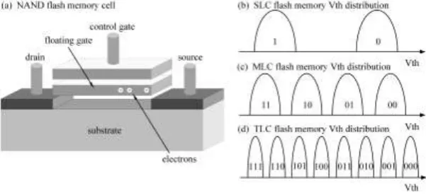
NAND flash memory is a type of non-volatile storage medium which is consist of floating gate (FG) transistors, the data of flash memory cells stored in the floating gate. The cross section of the flash memory cell is illustrated in Figure 1. During the program operation, the charge is injected into the floating gate by applying a high voltage to the control gate [1]. The isolated floating gate enables the retention of the charge for years. According to threshold voltage levels of cells, NAND flash can be divided into single-level cell (SLC) flash memory, multilevel cell (MLC) flash memory and triple-level cell (TLC) flash memory. Vth level distribution is shown in Figure 1.
Y. Cai [2] classified flash errors based on the cause of errors: erase error, program interference error, read error, and retention error. During read operation, the repeat reading operation on pages will result in read error in cells. In addition to the above situation, the occurrence of errors in NAND flash memory can also be determined by temperature [3].
Figure 1. (a) NAND flash memory cell; (b) SLC flash Vth distribution; (c) MLC flash Vth distribution; (d) TLC flash Vth distribution.
[image:1.595.146.447.522.660.2]1. We first describe the characterizations of errors in NAND flash memory under different situations: program disturbs, read disturbs, repeat P/E cycles, retention loss and high/low temperature.
2. We analyze the error mechanisms of four error types: program interference errors, read errors, erase errors and retention errors. And we find two conditions that mainly affect the error rate of flash memory.
3. We propose an adaptive error correction scheme to solve the problem that the ECC codes are unable to correct errors on the basis of error characteristics, an error correcting scheme that employs two types of error-correct methods adaptively to correct the different types of errors in the flash.
Error Characterization of NAND Flash Memory
NAND flash memory cells store data information from different Vth levels. Studying the threshold voltage distribution of error cell can give us a better understanding of error characteristic. The error characterizations also can be observed through raw bit error rate (RBER), which is the bit error rate in flash memory without error correcting scheme.
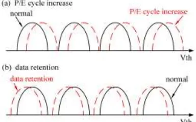
[image:2.595.202.394.410.530.2]Within the Flash lifetime limit, NAND flash memory undergoes a great number of program / erase cycles. After each P/ E cycle, the insulating properties of flash memory tunnel oxide are reduced, and the defects are accumulated in the tunnel oxide layer. Y. Cai[4] concluded that NAND flash threshold voltage distribution would shift to the right when the program/erase cycle increasing, as showed in Figure 2. After the threshold voltage distribution shifted to the right, flash memory read reference voltage keeps in constant; the state will be read as the adjacent state by NAND flash circuit. According to the test results of [5], the bit error rate increases non-linearly with the P/E cycling. Also, when data stored in the flash cell, the errors are more likely to occur in the storage cell over time at higher P/E cycles.
Figure 2.(a) Vth distribution before and after P/E cycles; (b) Vth distribution before and after data retention.
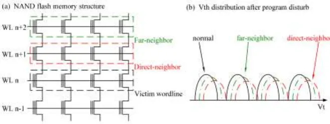
Besides the number of P/E cycles, the error characterizes of flash memory can also be influenced by the data programming location. During programming operations, the bias voltage applied to the cell in one word line may cause the current leak from the tunnel oxide into a nearby memory cell. Errors, in this case, are referred to as program interference errors. The NAND flash structure is shown in Figure 3. Program interference errors will become aggressive when the programming operations are continually applied to a wordline. Vth distribution offset of flash cells in a page caused by the adjacent cells is greater than the far-neighbor cells [6], shown in Figure 3.
During the read operation, high Vpass bias applied on the cells may lead SILC (Stress Induced Leakage Current) effects in other cells, would result in read disturb errors. As the reading cycles increasing, the threshold voltage distribution of cells shifts to the right according to the results of [7]. Y. Cai [7] also indicates that the bit error rate increases roughly linearly with the number of read operations, and the read disturb effects are greater at high P/E cycles.
Figure 3.(a) NAND flash memory structure; (b) Vth distribution after program disturb.
Temperature changes are also one of the important factors that need to be considered for flash memory reliability. In the high-temperature condition, the error rate of data retention error is higher than the error rate at room temperature. In the low temperature, the effects of P/E cycles are greater than the room temperature. We hypothesize that this is because that the number of defects accumulated in the floating gate under low-temperature condition is more than the defects at the room temperature.
Error Mechanism of NAND Flash Memory
In order to find a suitable solution of NAND flash memory reliability problems, it’s crucial to understand the error mechanism of flash memory besides the error characteristics. In NAND flash memory, the error characteristics can be simply represented by the bit error rate and the offset of Vth distribution, but the mechanisms behind these errors are complex. From the perspective of flash memory cells, we next explain the following error mechanisms of NAND flash memory.
Trap-assisted tunneling (TAT). During the P/E cycles, the high electric field stress applied to the tunnel oxide can lead to defects in the oxide layer. These structural defects form a leakage path in the tunnel oxide, and the charge leaks from the floating gate into the substrate. The TAT phenomenon is the origin of leakage current, SILC. The loss of charges in the floating gate causes the Vth distribution of flash memory cell shifts.
Random Telegraph Noise (RTN). Random Telegraph Noise is a low-frequency noise in the MOSFET devices, which can be characterized as a phenomenon that the fluctuations of the transistor drain current and the threshold voltage caused by the capture or emission of electrons at the oxide interface. In NAND flash memory, [1] indicates that Vth fluctuation drifts as the reading operation increases. The Vth fluctuation caused by RTN can be enhanced at high P/E cycles. Therefore, the effect of RTN on Vth can produce read errors especially when the number of P/E cycles increasing.
Disturb. When the density of flash memory cells is high, the continuous programming and reading operations can cause capacitive coupling phenomenon between storage units. When performing a reading operation, the high voltage Vpass is applied to cells that do not need to be read. With the high voltage, these cells gain charges, and the threshold voltage shifts to the positive direction. During the program operation, the program voltage can trigger the parasitic capacitance-coupling between cells in the same word line. The effect of disturbance will be aggressive when flash memory process is scaling down.
Adaptable Error-correct Scheme
In this section, we propose an adaptable error correction scheme to enhance the endurance of NAND flash memory devices. Our scheme is built on the error characterizes and the error mechanisms that we discussed above. This error correction scheme can be implemented into different NAND flash memory, such as the MLC flash memory and the TLC flash memory.
The main error-correct method in NAND flash memory is error-correcting code: LDPC code and BCH code. Recently, with the development of the manufacture process, BCH is unable to meet the error-correct requirement of NAND flash memory. The error correction capability of LDPC code is stronger than BCH code, but the implementation of LDPC can increase the latency of devices and cost a vast resource of hardware. Also, when performance of flash memory degrades, the ECC code can’t manage the errors caused by the various error mechanisms. To overcome these disadvantages of the ECC above, we designed an error-correct scheme on the basis of the error characterizations in the flash memory. By adopting two error-correct methods alternately, our scheme can extend the endurance of flash memory with low latency and resource-cost.
Depending on the discussion above, we can divide the flash memory errors into two parts: the errors occurred while P/E cycles increasing (mainly caused by the disturbs phenomenon between cells and the degradation of oxide) and data retention errors (mainly depending on the time that data stored in flash memory). It can be possible to conclude that the number of P/E cycles and the data storage time are two main conditions which determine the error rate in flash memory.
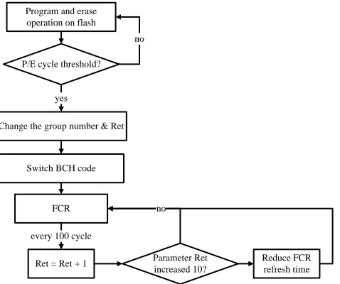
The key idea of the adaptable error correction scheme is to take different error correction strategy for the two kinds of errors above. Error correction methods we apply in this scheme are BCH code and FCR [9]. On consideration of hardware cost efficiency, we choose BCH code instead of LDPC code. The Flash Correct-and-Refresh (FCR) is an error correction technique which periodically reads pages in flash memory and reprograms the data into flash after correcting the errors. We first split the blocks in a flash into n groups. The number n is dependent on the storage size of flash memory. In this paper, we define 128 blocks as a group. And we label these groups according to the order of the block address as group1, group2, …, group n. Meanwhile, in order to quantify the effect of data retention at high P/E cycles, we use a parameter to indicate the effect which is named as Ret. The workflow of the error correction scheme is illustrated in Figure 4.
Program and erase operation on flash
P/E cycle threshold?
Change the group number & Ret yes
no
Switch BCH code
Ret = Ret + 1 Parameter Ret increased 10? every 100 cycle
FCR no
[image:4.595.180.419.502.702.2]Reduce FCR refresh time
Figure 4. Adaptable error correction scheme workflow.
When the P/E cycle number of the group with a minimum serial number reaches the threshold, the number of the group will be changed to the maximum serial number and the serial number of other groups will minus 1. And the BCH code implemented on the block group that reaches threshold value switches to a stronger one. For instance, a BCH code with t=10 shifts to the code with t=12.
As we analyzed before, the retention bit error rate increases faster with the P/E cycling. And this phenomenon becomes aggressive at higher P/E cycles. Based on this effect, after changing the value of group serial numbers, we set the value of parameter Ret to 1. Then the FCR operation is applied to the group with Ret value greater than 1. The parameter Ret plus 1 every 100 P/E cycles. The refresh time switches to the half of the previous one when the parameter Ret increases 10. The steps of this scheme above are executed cyclically through the entire lifetime of NAND flash memory.
Summary
We analyzed the characterizations of different types of errors in the flash memory, and explain the mechanisms behind these errors. On the basis of the analysis, we find two important conditions that mainly affect the error generation in flash memory: the number of P/E cycles and the data retention time. We propose a new adaptable error correction scheme, which is aimed to correct the errors caused by the increasing of P/E cycles and the data retention phenomenon. We hope our solution to enhance the endurance of NAND flash memory is able to be applied in future flash memory based devices.
Acknowledgement
We gratefully acknowledge the assistance of RECADATA Corporation.
References
[1] R. Micheloni, A. Marelli, R. Ravasio, Inside NAND Flash Memories, Springer, New York, 2010. [2] Yu Cai, Erich F. Haratsch, Onur Mutlu, Ken Mai, Error Patterns in MLC NAND Flash Memory: Measurement, Characterization, and Analysis, in: DATE, Dresden, 2012, pp. 521-526.
[3] H. Kameyama, Y. Okuyama, S. Kamohara, K. Kubota, H. Kume, K. Okuyama, Y. Manabe, A. Nozoe, H. Uchida, M. Hidaka, K. Ogura, A New Data Retention Mechanism After Endurance Stress On Flash Memory, in: IRPS, California, 2000, pp. 194-199.
[4] Yu Cai, Erich F. Haratsch, Onur Mutlu, Ken Mai, Threshold Voltage Distribution in NAND Flash Memory: Characterization, Analysis, and Modeling, in: DATE, Grenoble, 2013,pp. 1285-1290. [5] Eitan Yaakobi, Jing Ma, Laura Grupp, Paul H. Siegel, Steven Swanson, Jack K. Wolf, Error characterization and coding schemes for flash memories, in: Proc. Workshop on the Application of Communication Theory to Emerging Memory Technologies, Florida, 2010, pp. 1856-1860.
[6] Yu Cai, Onur Mutlu, Erich F. Haratsch, Ken Mai, Program Interference in MLC NAND Flash Memory: Characterization, Modeling, and Mitigation, in: ICCD, Asheville, 2013, pp. 123-130. [7] Yu Cai, Yixin Luo, Saugata Ghose, Onur Mutlu, Read Disturb Errors in MLC NAND Flash Memory: Characterization, Mitigation, and Recovery, in: DSN, Rio de Janeiro, 2015, pp. 438-449. [8] Yu Cai, Yixin Luo, Erich F. Haratsch, Ken Mai, Onur Mutlu, Data Retention in MLC NAND Flash Memory: Characterization, Optimization, and Recovery, in: HPCA, California, 2015, pp. 551-563.