Frequency Generation Techniques
for Integrated Applications
Thesis by
Roberto Aparicio Joo
In Partial Fulfillment of the Requirements
for the Degree of
Doctor of Philosophy
California Institute of Technology
Pasadena, California
2004
Roberto Aparicio Joo
All Rights Reserved
iii
Acknowledgements
First, I would like to thank my advisor, Prof. Ali Hajimiri, for giving me the invaluable opportunity to study under his tutelage and work in his research group at Caltech. His support, guidance and advice have made this thesis possible.
I am also grateful to Prof. David Rutledge for his support and kind personal assistance. I would like to thank the committee members of my candidacy exam: Prof. Jehoshua Bruck, Prof. Michael Roukes, Prof. Kerry Vahala, and Dr. Sander Weinreb for giving me valuable feedback and insights that I used in the later stages of my work.
I also want to thank my Ph. D. defense committee members, Prof. Jehoshua Bruck, Prof. Yu-Chong Tai, Prof. Kerry Vahala, and Dr. Sander Weinreb, for their time.
I appreciate the financial assistance from the sponsors of my research at Caltech. Conexant Systems (now Skyworks Solutions Inc.) and Jazz semiconductors for chip fabrication, in particular I thank Rahul Magoon, Frank Int’veld, Terry Whistler, and Steve Lloyd of Skyworks Solutions and Marco Racanelli, Arjun Kar-roy, Scott Stetson and Marion Knight of Jazz Semiconductor for consistent support and help. I acknowledge the Fullbright fellowship and Conacyt during my first year as a Ph.D. student, and the IBM Corporation graduate fellowship during my fourth year and the assistance of Dr. Modest Oprysko and Dr. Mehmet Soyuer with that regard. Other sponsors of my research include The Lee Center for Advanced Networking at Caltech, the Caltech Center for Neuromorphic Systems Engineering (CNSE), National Science Foundation (NSF), and Xerox Corporation.
I would not be at this stage of my life if I had not come across some of the most influential persons in my academic life: Professors Alejandro Pedroza Melendez and Domingo Vera Mendoza. What I learned from them goes well beyond pure academics.
I am also thankful to my colleagues and friends at Caltech: Ehsan Afshari, Behnam Analui, Dr. Ichiro Aoki, Diego Benitez, Jim Buckwalter, Xiang Guan, Prof. Donhee Ham, Prof. Hossein Hashemi, Oliver Henry, Daniel Katz, Dr. Scott Kee, Abbas Komijani, Milan Kovacevic, Christopher Lee, Dai Lu, Sam Mandegaran, Anselmo Martinez, Dr. Mathew Morgan, Arun Natarajan, Eric Oestby, Ann Shen, Takahiro Taniguchi, Dr. Ivan Veselic, Niklas Wadefalk, Jean Wang, Christopher White, and Prof. Hui Wu.
I would also like to thank Fr. Andrew Mulcahey and the Legion of Christ for their continuos support and help during the most difficult times of my life.
I am specially grateful to my family, my father Roberto, my sister Masue, my aunt Narda Oliva and uncles Ruben and Rodulfo, for their unconditional support and love.
To my mother Silvia, whose love has never faltered for an instant since the day I was born. It is impossible to express her my gratitude in such a short space. Mama, I love you with all my heart.
v
Faciendi plures libros nullus est finis frequensque meditatio carnis afflictio est. Liber Ecclesiastes 12,12
Abstract
This thesis presents novel oscillator topologies and passive structures that demonstrate improvements in performance compared to existing devices in CMOS. The contributions of this work include the development of original topologies and concepts together with practical implications in the area of integrated frequency generation.
A noise-shifting differential Colpitts oscillator topology is proposed. It is less sensitive to noise generated by the active devices than commonly used integrated oscillator topologies such as NMOS- or PMOS-only, and complementary cross-coupled. This is achieved through cyclostationary noise alignment while providing a fully differential output and large loop gain for reliable start up. An optimization strategy is derived for this oscillator that is used in the implementation of a CMOS prototype. The performance of this oscillator is compared to traditional topologies and previously published integrated oscillators achieving lower phase noise and some of the highest figures of merit, respectively.
A new circular-geometry oscillator topology is introduced. It allows the implementation of slab inductors for high-frequency and low-phase noise oscillator applications. Slab inductors present an attractive alternative for monolitic applications where low loss, low impedance, and high self-resonance integrated inductors are required. A general methodology to ensure the proper oscillation mode when several oscillator cores are coupled in a circular-geometry as well as to achieve a stable dc bias point is offered. Several circular-geometry CMOS integrated oscillator prototypes are presented as a proof of concept and their performances are compared to previously published high frequency oscillators achieving some of the best figures of merit.
vii
This study leads to two new capacitor structures with high lateral-field efficiencies. These new capacitors demonstrate larger capacities, superior matching properties, tighter tolerances, and higher self-resonance frequencies than the standard horizontal parallel plate and previously reported lateral-field capacitors, while maintaining comparable quality factors. These superior qualities are verified by simulation and experimental results.
ix
Table of Contents
Acknowledgements
iii
Abstract ... v
List of Tables ... xi
List of Figures ... xiii
Chapter 1: Introduction
1
1.1 Motivation ... 11.2 Organization of the Dissertation ... 4
Chapter 2: Frequency Generation Fundamentals
7
2.1 Frequency Synthesis Techniques ... 102.2 Coherent Indirect or Phase-Locked-Loop Frequency Synthesis... 12
2.2.1 Phase-Locked-Loop Basics ... 13
2.3 Phase-Locked-Loop Spectral Purity ... 15
2.4 Oscillator Phase Noise ... 19
2.5 Challenges in Integrated Oscillator Design... 23
2.6 Summary ... 23
Chapter 3: A Noise Shifting Colpitts VCO
25
3.1 Oscillator Topology Comparison ... 263.2 Design Evolution... 32
3.3 Design Example ... 36
3.3.1 Inductor and Varactor Optimization ... 36
3.3.2 Process Technology, Design Equations and Constraints ... 40
3.3.3 Graphical Optimization Methods and Inductance Selection ... 46
3.4 Experimental Results ... 51
3.5 Summary ... 57
4.1 On-chip Inductors... 60
4.2 Circular Geometry Oscillators ... 66
4.3 Magnetic Coupling... 69
4.4 Design examples ... 70
4.5 Summary ... 75
Chapter 5: Quadrature Signal Generation
77
5.1 Introduction ... 775.2 IQ Generation by Frequency Division ... 79
5.3 Quadrature Coupled Oscillators... 81
5.3.1 Experimental Results ... 90
5.4 Polyphase Filter Quadrature Signal Generation... 94
5.5 Summary ... 95
Chapter 6: Capacity Limits and Matching Properties of Integrated
Ca-pacitors
97
6.1 Introduction ... 986.2 The Effect of the Density on Other Capacitor Properties ... 101
6.3 Capacity Limits ... 102
6.4 Purely-Lateral Field Capacitive Structures ... 107
6.5 Capacitance Comparison... 112
6.6 Measurement Results ... 119
6.7 Summary ... 127
Chapter 7: Closed Loop Frequency Generation
129
7.1 A 6.6GHz Phase-Locked-Loop for Concurrent Dual-Band Receiver Applications129 7.1.1 Receiver Architecture and Frequency Planning ... 1307.1.2 PLL Building Blocks ... 132
7.1.2.1 Voltage Controlled Oscillator ... 133
7.1.2.2 Frequency Dividers ... 133
7.1.2.3 Phase Detector and Charge Pump ... 134
7.1.2.4 Loop Filter... 136
7.1.3 Experimental Results ... 138
7.2 An Ultra-Low-Power 6.4GHz PLL... 139
7.2.1 System Blocks ... 139
7.2.2 Simulation Results and Power Consumption Comparison... 140
7.3 A Phase-Compensated Fractional-N PLL... 141
7.3.1 Spur Reduction Techniques in Fractional-N Frequency Synthesis ... 142
Table of Contents xi
7.3.2.1 Delay Locked Loop... 147
7.3.2.2 PLL Building Blocks... 148
7.3.3 Simulation Results and Comparison... 149
7.4 Summary ... 150
Chapter 8: Conclusion
151
8.1 Summary ... 1518.2 Recommendations for Future Investigations ... 153
xiii
List of Tables
Chapter 1: Introduction
Chapter 2: Frequency Generation Fundamentals
Chapter 3: A Noise Shifting Colpitts VCO
Table 3.1: Phase noise contribution of each noise source...29
Table 3.2: Oscillator comparison. ...31
Table 3.3: NMOS transistor model values...41
Table 3.4: Initial design variables. ...43
Table 3.5: Reduced set of design variables...47
Table 3.6: Specific design constraints...47
Table 3.7: Component values for the implemented noise shifting differential Col-pitts VCO. ...52
Table 3.8: Oscillator comparison. ...55
Chapter 4: Circular-Geometry Oscillators
Table 4.1: Typical silicon process technology...63Table 4.2: Circular-geometry oscillators performance summary. ...74
Table 4.3: Oscillators above 4GHz comparison. ...75
Chapter 5: Quadrature Signal Generation
Chapter 6: Capacity Limits and Matching Properties of Integrated
Ca-pacitors
Table 6.1: Capacitance comparison. ...119Table 6.2: Measurement results - first set. ...121
Table 6.3: Measurement results - second set (1pF). ...123
Table 6.4: Measurement results - second set (10pF). ...126
Table 7.1: Concurrent receiver frequency planning... 132
Table 7.2: Low power 6.4GHz PLL performance summary... 140
Table 7.3: Fully integrated low-power PLLs comparison... 141
Table 7.4: 3.2GHz phase-compensated PLL performance summary... 150
xv
List of Figures
Chapter 1: Introduction
Figure 1.1: Breakdown of silicon and GaAs technologies in the total and RF
semi-conductor revenue...2
Chapter 2: Frequency Generation Fundamentals
Figure 2.1: Oscillator output spectrums, a) ideal, b) typical. ...7Figure 2.2: Simplified model of a generic transceiver. ...8
Figure 2.3: Downconversion by a noisy oscillator, a) RF spectrum, b) IF spectrum. 9 Figure 2.4: Effect of phase noise in transmitters...9
Figure 2.5: Incoherent frequency synthesis method...10
Figure 2.6: Direct digital synthesis...10
Figure 2.7: Coherent frequency synthesis method. ...11
Figure 2.8: Coherent indirect frequency synthesis or phase-locked-loop. ...12
Figure 2.9: Phase-locked-loop state variable diagram. ...13
Figure 2.10: Frequency representation of oscillator phase noise. ...15
Figure 2.11: Phase-locked-loop feedback system. ...16
Figure 2.12: Phase-locked-loop phase noise transfer characteristics, a) VCO noise, b) reference noise...18
Figure 2.13: ISF and output voltage waveforms of a typical LC oscillator. ...20
Figure 2.14: Drain current and a sample of the channel noise in a MOS transistor.21 Figure 2.15: Oscillator tank voltage vs. bias current of a typical LC oscillator...22
Chapter 3: A Noise Shifting Colpitts VCO
Figure 3.1: NMOS-only cross-coupled oscillator: a) Circuit schematic, b) ISF, NMF and effective ISF waveforms...26Figure 3.2: Complementary cross-coupled oscillator: a) Circuit schematic, b) ISF, NMF and effective ISF waveforms...27
Figure 3.3: Single-ended Colpitts oscillator topology: a) Circuit schematic, b) ISF, NMF and effective ISF waveforms...27
Figure 3.5: Current switching topology evolution a) Timed switch implementation
b) NMOS transistors implementation. ... 34
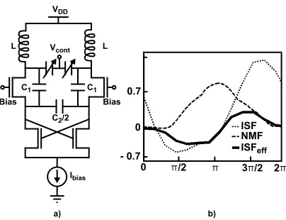
Figure 3.6: Noise shifting differential Colpitts VCO a) Final topology, b) ISF, NMF and effective ISF waveforms for the core transistor... 35
Figure 3.7: Capacitance behavior of a pn-junction varactor... 37
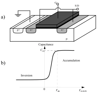
Figure 3.8: MOS varactor a) cross section of a NMOSCAP, b) capacitance behav-ior vs. VG,S/D. ... 38
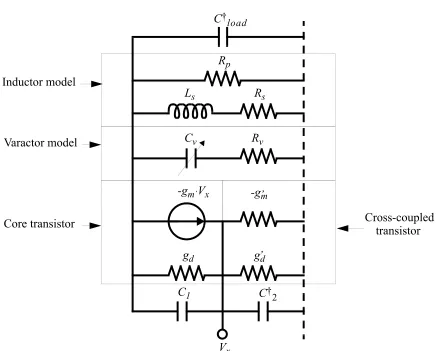
Figure 3.9: NMOS transistor model. ... 41
Figure 3.10: MOS varactor equivalent circuit model ... 42
Figure 3.11: Integrated spiral inductor model. ... 42
Figure 3.12: Equivalent noise shifting differential Colpitts oscillator model... 44
Figure 3.13: Design constraints for C1 = 0.4pF, w’=100mm and Ls= 2.4nH. ... 48
Figure 3.14: Design constraints for C1 = 0.6pF, w’=100mm and Ls= 2.4nH. ... 49
Figure 3.15: Design constraints for C1 = 0.4pF, w’=300mm and Ls= 2.4nH. ... 50
Figure 3.16: Circuit schematic of the implemented noise shifting differential Col-pitts oscillator. ... 51
Figure 3.17: Differential Colpitts oscillator die micrograph. ... 52
Figure 3.18: Differential Colpitts oscillator frequency tuning. ... 53
Figure 3.19: Measured phase noise vs. offset frequency at 1.8GHz ... 54
Figure 3.20: PFN for previously published oscillators... 56
Figure 3.21: PFTN for previously published oscillators. ... 57
Chapter 4: Circular-Geometry Oscillators
Figure 4.1: Different choices of integrated inductors, a) multi-turn spiral, b) sin-gle-turn spiral, c) slab... 61Figure 4.2: Single-turn and slab inductor comparison... 62
Figure 4.3: Inductor comparison vs. inductance value, a) quality factor Q, b) self-resonance frequency... 64
Figure 4.4: Slab inductor terminal connection issues... 65
Figure 4.5: Proposed oscillator topology. ... 66
Figure 4.6: dc latching issues... 67
Figure 4.7: Undesirable oscillation modes, a) block diagram, b) equivalent sche-matic... 68
Figure 4.8: Proposed oscillator topology. ... 69
Figure 4.9: Single-frequency circular-geometry oscillator die micrograph. ... 71
Figure 4.10: Single-frequency Circular-Geometry oscillator phase noise plot at fosc=5.35GHz ... 72
Figure 4.11: Voltage controlled circular-geometry oscillator frequency tuning... 73
Chapter 5: Quadrature Signal Generation
Figure 5.1: Hartley image-reject receiver. ... 78List of Figures xvii
duty cycle mismatch on the quadrature accuracy. ...80
Figure 5.4: Quadrature-coupled LC VCO, a) circuit topology, b) block diagram. 82 Figure 5.5: Quadrature-coupled oscillator system. ...83
Figure 5.6: RC circuit implementation...84
Figure 5.7: Amplitude and phase noise degradation vs. the coupling factor...86
Figure 5.8: Amplitude and phase mismatch vs. the coupling factor for a tank referred capacitor of 2%. ...87
Figure 5.9: Amplitude and phase mismatch vs. the tank referred capacitor for ....88
Figure 5.10: Quadrature NMOS-only cross-coupled oscillator die photo. ...90
Figure 5.11: Quadrature NMOS-only cross-coupled oscillator frequency tuning. ..91
Figure 5.12: Measure phase noise vs. offset frequency at 1.72GHz. ...92
Figure 5.13: RC polyphase network...93
Figure 5.14: Polyphase filter used as quadrature signal generator. ...94
Chapter 6: Capacity Limits and Matching Properties of Integrated
Ca-pacitors
Figure 6.1: Parallel Plate capacitor...99Figure 6.2: Parallel Wires configuration. ...100
Figure 6.3: Dimensions of the metal lines...103
Figure 6.4: Parallel Plate structures normal to the cartesian axis...104
Figure 6.5: Ortho-normal decomposition into lateral and vertical parallel plates... 106 Figure 6.6: Vertical Parallel Plates structure. ...108
Figure 6.7: Vertical Bars structure...109
Figure 6.8: Modified Vertical Bars structure...110
Figure 6.9: Modified Vertical Parallel Plates structure. ...111
Figure 6.10: Manhattan capacitor structures: a) Parallel Wires (PW), b) Woven, c) Woven no Via, and d) Cubes 3-D. ...112
Figure 6.11: Quasi-fractal capacitor structures. ...113
Figure 6.12: Capacitance density vs. minimum lateral dimensions for tox = tmetal = 0.8µm. ...115
Figure 6.13: Field usage efficiencies for , and . ...117
Figure 6.14: Capacitance densities for and . ...118
Figure 6.15: Die micrograph of the first test capacitor for Lmin = Wmin = 0.5mm ... 120 Figure 6.16: Capacitance distribution of the VPP, PW, and HPP structures. ...122
Figure 6.17: Die micrographs of the second test capacitors for Lmin = Wmin = 0.24mm. ...123
Figure 6.18: High-frequency admittance measurement results for the HPP, VB, and VPP structures...125
Figure 7.1: Dual-band receiver architecture. ... 130
Figure 7.2: Frequency allocation and planing for the dual-band receiver. ... 131
Figure 7.3: 6.6GHz PLL block diagram. ... 132
Figure 7.4: NMOS-only cross-coupled voltage controlled oscillator... 133
Figure 7.5: Divide-by-two master-slave flip-flop, a) block diagram, b) circuit sche-matic... 134
Figure 7.6: Phase-frequency detector schematic. ... 135
Figure 7.7: Charge-pump circuit schematic... 136
Figure 7.8: Loop filter schematic... 137
Figure 7.9: Dual-band concurrent receiver die photo... 138
Figure 7.10: Fractional-N frequency synthesis, a) block diagram, b) timing diagram for division. ... 142
Figure 7.11: DAC estimation method... 143
Figure 7.12: Phase compensation method, a) block diagram, b) on-chip tuning achieved with a DLL... 145
Figure 7.13: Phase-compensated PLL timing diagram for division. ... 146
Figure 7.14: Modified DLL block diagram operating at one fourth the data rate.147 Figure 7.15: Delay element block diagram... 148
Figure 7.16: Dual-modulus prescaler architecture... 149
Chapter
1
1
Introduction
The end of the twentieth century and the beginning of the twenty-first century will be
remembered by the tremendous growth of mobile communications. Driven by economical
and technological forces, small and low-cost handheld devices have invaded the market.
For instance, mobile phone sales totaled 115 million units in the second quarter of 2003,
where as the 2004 global cell phones sales is expected to top 500 million units. This is
mainly because of the demand for mobile phones with E-mail and Internet access
capabilities, and models with integrated digital cameras, FM tuners, MP3 music players,
personal digital assistants (PDA) and other commodities [1].
Technology improvements and market growth have been pushing for higher quality of
service in transmission and reception of information at faster data rates. For example, third
generation (3G) communication systems enable high-speed data communication, mobile
Internet, E-mail, video on demand, and E-commerce. Also, short-range wireless local area
networks (WLAN) have emerged, leading to standards such as the IEEE802.11a and its
European counterpart HIPERLAN, that target for 54Mbps at 5GHz, while the IEE802.11b
and the recent IEEE802.11g enable data rates of 11Mbps and 22-50Mbps, respectively, at
2.4GHz. The variety of wireless standards and communication methods will continue to
present major challenges for telecommunication design engineers.
1.1
Motivation
Economy of sale forces the phone manufacturers to integrate as many of the elements
continues ultimately towards the single-chip mobile radio. To accomplish this,
architectural and technological integration innovations are required.
There are several benefits obtained from a higher degree of integration. The absence of
external nodes reduces package parasitics, interference, noise, and signal coupling. Fewer
external nodes translate to a smaller package size with less pin number count, thus leading
to an smaller system. Lower power consumption is also achieved since there is no need for
off-chip signal buffering. Higher predictability and repeatability are an important benefit
of higher levels of integration. Additionally, higher integration reduces the number of
external components that lower the manufacturing costs considerably.
Although GaAs technology has been used to implement RF circuits, CMOS
technology can be applied to RF circuits [2]-[4]. The higher yield and reliability of silicon
technologies increases the number of available transistor on a single chip, generating new
possibilities not conceivable in GaAs or other III-V technologies. CMOS technology is
particularly promising as the wafer manufacturing costs of CMOS are much lower than
GaAs. Moreover, fierce competition between CMOS foundries is expected, which will
further reduce these costs. These are mainly because over 97% of the total semiconductor All Semiconductor
Devices
RF Devices
2%
$130 Billion
RF Devices
Silicon 60% $2.5 Billion
GaAs Discrete 20% GaAs IC
20% Silicon
~97%
1.1. Motivation 3
devices produced worldwide are manufactured in CMOS technology [5] (Figure 1.1). On
the other hand, GaAs only occupies about 1% of the market share. Therefore, aggressive
cost reduction and heavy competition has been experienced by silicon technology over the
last several years and is expected to continue.
For certain RF applications, pure CMOS technology may not be suitable. For some of
these applications, technologies such as SiGe-BiCMOS have been introduced as
alternatives for applications that require higher performances. These more specialized
processes increase the manufacturing costs by 10% to 50% due to the extra processing
steps required for the availability of NPN transistors, MIM capacitances, resistors, and
thick top metal layers [6]. Although the NPN transistors available in SiGe-BiCMOS
technology can be faster, the lack of competition in this industry compared to CMOS
would make it unlikely that the price will decrease resulting in a solution not as
cost-effective as CMOS technology.
One of the major challenges towards the integration of the CMOS-only radio is the
frequency generation block. The spectral purity of the local oscillator signals is one of the
most critical parameters affecting the reliability and quality for the transfer of information
in this radio [7][8]. Unfortunately, there are several obstacles that can deteriorate the
performance of CMOS oscillators. The transistor devices readily available in these
process technologies generate high active device noise due to short channel and hot
electron effects [9]. Therefore, these circuits suffer from a worse noise performance than
modules fabricated using discrete components. Also, the driving force in CMOS
technologies are digital applications, therefore, these technologies are not optimized for
analog or RF applications. Furthermore, to avoid latch up of the digital circuits, the silicon
substrate is fairly conductive and increases the signal loss because of the energy coupled,
both inductively and capacitivelly, into the substrate, resulting in lossy passive
With the goal of overcoming these drawbacks of CMOS technology, novel circuit
topologies and passive structures will be presented in this dissertation. These new
structures demonstrate significant improvements in performance compared to existing
devices in CMOS.
1.2
Organization of the Dissertation
After reviewing the traditional frequency generation fundamentals, a brief overview of
the coherent indirect frequency synthesis basics will be explained in Chapter 2. We will
then focus on the spectral purity of phase-locked-loops (PLL) and local oscillators as well
as the integration challenges imposed by silicon technology with further detail.
Chapter 3 compares the existing oscillator topologies with an emphasis on the
cyclostationarity of noise sources and presents the design evolution leading to a topology
that lowers the phase noise through cylostationary noise alignment. This new topology
provides a fully differential output and a large loop gain for reliable start up. A design
strategy is also devised for this oscillator and the phase noise performance of a CMOS
prototype is compared to previously published integrated oscillators achieving some of the
highest figures of merit.
A new circular-geometry oscillator topology that allows the implementation of slab
inductors for high frequency integrated applications is presented in Chapter 4. Slab
inductors present an attractive alternative for monolitic applications where low impedance
and high quality factor integrated inductors are required. A general methodology to ensure
the proper oscillation mode when several oscillator cores are coupled in a
circular-geometry is also introduced. Several circular-geometry CMOS integrated
oscillator prototypes are presented as a proof of concept and their performance is
compared to previously published high frequency oscillators achieving some of the best
1.2. Organization of the Dissertation 5
An overview of the existing methods for generating on-chip in-phase and quadrature
(IQ) signals is presented in Chapter 5 with an emphasis on coupled oscillators. The
trade-off between the phase noise performance and the quadrature and in-phase signal
accuracy will be investigated and a general design methodology is devised to optimally
couple quadrature oscillators. A CMOS oscillator prototype optimized using this
methodology is fabricated and its phase noise enhancement is verified experimentally.
Capacitors are essential components in several analog integrated circuits as well as
radio frequency (RF) building blocks. In many of these applications, the capacitor
tolerance and matching properties play an essential role in determining their performance.
In some other of these applications, capacitors with large values are needed. Often,
off-chip capacitors are required as the integrated on-chip capacitor would consume a large
die area. In Chapter 6, theoretical limits for the capacitance density of integrated
capacitors with combined lateral and vertical field components are derived. These limits
are used to investigate the efficiency of various capacitive structures such as lateral flux
and quasi-fractal capacitors. This study leads to two new capacitor structures with superior
matching properties and high lateral-field efficiencies. These new capacitors demonstrate
larger capacities, superior matching properties, tighter tolerances, and higher
self-resonance frequencies than the standard horizontal parallel plate and previously
reported lateral-field capacitors, while maintaining comparable quality factors. These
superior qualities are verified by simulation and experimental results.
Integrated phase-locked-loops will be presented in Chapter 7. First, the
implementation of a triple-frequency output PLL will be presented. A frequency planning
scheme that allows the generation of three local oscillator signals using only one PLL will
be discussed. These three local oscillator signals are required for simultaneous
downconversion to base band in a dual-band CMOS concurrent receiver [9]. Then, the
design challenges in the design of an ultra-low-power PLL prototype implemented in a
will be introduced that attenuates the fractional spur in an integrated fractional-N PLL for
low-power integrated applications.
A summary of the results presented in this dissertation as well as suggestions for
Chapter
2
7
Frequency Generation
Fundamentals
An indispensable building block required for both the receive and transmit path in
modern communications systems is the phase-locked-loop (PLL). PLLs can be used to
maintain a well-defined phase and frequency relation between two signal sources.
Therefore, they can provide a stable local oscillator output required for frequency
translation, modulation, and demodulation. Due to their remarkable versatility, PLLs are
usually preferred over other methods of maintaining phase lock, as will be discussed
shortly.
Local oscillator’s short-term instabilities directly affect the quality and reliability of
the information being transferred. It is therefore important to review some of the
underlying properties of the local oscillator noise and their effect in the transmit and
receive path.
Local oscillators are susceptible to noise injected either by its constituting devices or
by external sources. These noise sources would influence both the frequency or phase and
amplitude of the output. Ideally, the output of the local oscillator can be expressed as:
(2.1)
ωo ω ωo ω
Figure 2.1: Oscillator output spectrums, a) ideal, b) typical.
a) b)
where the amplitude Vo, frequency and phase are all constants. The one-sided spectrum of this ideal oscillator consists of an impulse at frequency , as depicted in Figure 2.1a. However, due to the abovementioned random fluctuations, the output of a real oscillator can be more generally expressed as:
(2.2)
where and are both functions of time and f represents the periodic waveform of the steady-state output of the oscillator. If is not a pure sinusoid, the oscillator spec-trum has components around the harmonics of . What is more, due to the fluctuations represented by and , the spectrum of the oscillator has side bands close to the frequency of oscillation , as shown in Figure 2.1b. These skirts in the spectrum are generally referred to as phase noise side bands. To help us understand the importance of phase noise, consider a generic RF transceiver shown in Figure 2.2. It consists of a low noise amplifier (LNA), power amplifier (PA), filters, mixers, and a frequency synthesizer that provides the carrier signal (local oscillator) for both the receiver and transmit paths.
If the local oscillator output has a large phase noise, the up- and down-converted
signals are corrupted. Suppose the signal of interest is to be received in the presence of a
strong interferer in the form of an adjacent channel. Consequently, some downconversion
of these two signals will occur in the receive path. The resulting spectra will consist of two
overlapping signals, as depicted in Figure 2.3. As can be seen, the desired signal can get
ωo φo
ωo
Vout( )t = Vo⋅[1+A t( )]⋅f[ωot+φ( )t ]
A t( ) φ( )t
f t( )
ωo
A t( ) φ( )t
ωo
Figure 2.2: Simplified model of a generic transceiver. Duplexer
LNA Filter
Frequency Synthesizer
(LO)
Filter PA
Antenna
. 9
buried under the interferer which can significantly degrade the dynamic range of the
receiver.
As for the transmit path, the phase noise will generate interference around the local
oscillator output frequency, corrupting the neighboring channels, as depicted in
Figure 2.4. Therefore, improving the phase noise of the local oscillator improves the
performance of both receiver and transmitter.
In this chapter, we will start with a brief overview of the traditional frequency
generation techniques. Then, the basics of the coherent indirect frequency synthesis will
be covered. Finally, we will review the spectral purity of phase-locked-loops (PLLs) and
voltage controlled oscillators.
ωLO ω
Desired Signal Strong
Adjacent Channel LO
Figure 2.3: Downconversion by a noisy oscillator, a) RF spectrum, b) IF spectrum. a)
ωIF ω
b)
Desired Signal Interferer
ω1 ω
Adjacent Channel Transmitter
ω2
2.1
Frequency Synthesis Techniques
The term frequency synthesis was first introduced by Finden in 1943 [11]. The first
generation of frequency synthesizers used an incoherent method. In this approach, the
frequencies were synthesized by manually switching and mixing several crystal oscillators
and filters [12], as shown in Figure 2.5.
The ever increasing need for frequency generation schemes with higher accuracy,
stability, and versatility than the incoherent method have resulted in three options for
frequency synthesis in todays communication systems, namely, table-look-up, coherent
and indirect frequency synthesis (phase-lock) [12].
In a digital synthesizer (table-look-up), the output sinusoid is generated using the
digital values of the waveform stored in a memory, as depicted in Figure 2.6. The signal is
generated in the form of a series of digital numbers with clock frequency fref and a f1
f2
f3
f4
xN
Filter fo
Figure 2.5: Incoherent frequency synthesis method.
fo = N x fi + fj i, j =1, 2, 3, 4
Figure 2.6: Direct digital synthesis.
K Phase
accumulator Sinetable DAC Filter fo
2.1. Frequency Synthesis Techniques 11
digital-to-analog converter (DAC) is required to process the data from the memory
containing the sine or cosine values. These values are set by the accumulator and 2N clock
cycles are required for completion of one full cycle. Thus, corresponding to an output
frequency of with an N-bit accumulator. Here, the accumulator capacity
determines the frequency resolution. A low pass filter is usually required to remove the
high-frequency spurs generated by this digital process. The table-look-up method features
fine frequency resolution, very fast settling time, and low harmonic and spur content.
However, it suffers from the limited speed of the memory and the resolution and speed of
the digital-to-analog converter. Also, the output frequency is always lower than half the
reference frequency based on the Nyquist criterion. All these issues limit their use to few
hundreds of megahertz for fully integrated applications [13]-[15]. Hence, high frequency
of operation is not feasible.
The coherent frequency synthesis method shown in Figure 2.7 has also been used in
the past. In this approach, various output frequencies are generated with the combination
of frequency multipliers, dividers, and mixers. Thus, high frequency accuracy is
attainable. Ideally, the stability and accuracy of the output frequencies are the same as
those of the reference signal. However, undesired sidebands and high cross-talk between
stages are a serious problem for practical monolitic implementations that directly impact
the spectral purity of the output. Another disadvantages are the stringent filtering fref⁄2N
fref
N
÷
fo1
fo2
fo3
fo4 fo1 = M1M2 fref
fo2 = (M1M2 + M3/N) fref fo3 = (M1 + M1M2 + M3/N) fref fo4 = (M1 + M1M2 + 2M3/N) fref
Figure 2.7: Coherent frequency synthesis method.
M
1×
×
M
2M
3requirements and the large number of blocks and components, which causes the direct
synthesizer to be bulky and power hungry. These drawbacks limit its practical use for
integrated applications.
Modern frequency synthesizers for portable applications use an indirect method
known as a phase-lock technique shown schematically in Figure 2.8. This coherent
indirect frequency synthesis generates the output by phase-locking the divided output to a
reference signal and has the potential of combining high frequency and low power and is
well suited for integration in low-cost CMOS processes.
2.2
Coherent Indirect or Phase-Locked-Loop
Frequency Synthesis
Monolitic PLLs have been widely used in wired and wireless communications, as well
as digital and control systems. Their applications span from frequency synthesis,
modulation and demodulation of signals, data and signal recovery, and clock generation
and distribution among others. The first description of a phase-locked-loop was provided
by H. de Bellescize in 1932 [16]. In this work, an architecture consisting of an oscillator,
mixer and amplifier was proposed for demodulating and receiving AM signals. The local
oscillator was required to be tuned at exactly the same frequency as that of the incoming fref
Phase
detector Loopfilter
VCO
fout
Frequency divider
/N
Figure 2.8: Coherent indirect frequency synthesis or phase-locked-loop. fdiv
2.2. Coherent Indirect or Phase-Locked-Loop Frequency Synthesis 13
carrier. Thus, it was essential for the local oscillator to be in phase with the carrier for
maximum output. In other words, this local oscillator had to be phase-locked by a
phase-locked-loop. Some other early applications that use PLLs include synchronization
of the image and color bursts for TVs, and tuning of stations in FM radios.
2.2.1 Phase-Locked-Loop Basics
In this section, a brief overview of some of the basic properties of PLLs is offered. A
general PLL consists of four basic components, namely the phase detector (PD), loop
filter with transfer function Glf(s), voltage controlled oscillator (VCO) and an optional
frequency divider, as depicted in Figure 2.8. In this scheme, the output frequency of the
VCO is divided by N in the frequency divider block. The divided signal phase is then
compared in the phase detector block to that of the reference. This reference signal is
usually generated by an external source which has a high signal-to-noise ratio and is very
clean and stable. Under the locked condition, the negative feedback adjusts the control
voltage of the VCO in such a way that the reference and the divided signal have a constant
phase difference. Therefore, these two signals have the same frequencies.
When the phase relationship between and is constant, the PLL is in lock and
the output frequency equals the divided frequency, i.e., or,
(2.3) VCO
Figure 2.9: Phase-locked-loop state variable diagram.
Glf( )s θout
N
÷
θdiv
θref + vpd vc
_
Σ
fref fdiv
fdiv = fref
Even though the phase-locked-loop is a non-linear system, it can be modeled quite accu-rately as a linear time-invariant system when in lock [17]-[21]. This is mainly because the phase detector transfer characteristic is linear in phase domain under lock. A simple way to analyze this system is by using the phases of the reference and the output of the VCO signals as loop variables, as shown in Figure 2.9.
The input signal and the output of the PLL have phases and ,
respectively. The divider block divides the VCO frequency by a factor N, therefore, it also
divides its phase by the same factor:
(2.4)
When the loop is locked, or close to be locked, the phase detector output voltage is propor-tional to the phase difference between its inputs, i.e.,
(2.5)
where is the phase detector gain and has units of [V/rad]. This phase difference or error, vpd, is filtered by the low-pass transfer function of the loop filter , which attenuates noise and high frequency components. has an important effect on the noise characteristics of the loop as will be discussed shortly.
The output frequency of the VCO is proportional to its control voltage, vc. Since the
phase is the integral of the frequency, the VCO acts as an ideal integrator for the input
voltage vc. The output phase can then be found by integrating the VCO output frequency,
i.e.,
(2.6)
where is the VCO gain factor with units [rad/V s]. By applying the Laplace trans-form to (2.6), we obtain:
(2.7)
θref( )t θout( )t
θdiv( )t θout( )t N ---=
vpd( )t = Kpd⋅[θref( ) θt – div( )t ]
Kpd
Glf( )s Glf( )s
θout( )t =
∫
t Kvco⋅vc( )t ⋅dtKvco
θout( )s Kvco⋅Vc( )s
2.3. Phase-Locked-Loop Spectral Purity 15
The phase domain equivalent system of the PLL depicted in Figure 2.9 can be viewed
as a standard feedback system with a forward transfer function
and a feedback gain, . The phase domain
transfer function of this PLL is then:
(2.8)
2.3
Phase-Locked-Loop Spectral Purity
Although there are several ways to quantify the frequency instabilities of a local
oscillator, we will focus on the most common measure for their spectral purity, namely
phase noise. The single sideband noise spectral density is defined as,
(2.9)
where is the noise power in the band at an offset frequency from the carrier, per unit bandwidth, as depicted in Figure 2.10
G s( ) = Kpd⋅Glf( )s ⋅KVCO⁄s H s( ) = 1⁄N
θout( )s
θref( )s
--- G s( ) G s( )⋅H s( )+1
--- N K⋅ pd⋅KVCO⋅Glf( )s Kpd⋅KVCO⋅Glf( )s +N s⋅
---= =
L{∆ω} 10 Psideband(ωo+∆ω,1Hz) Pcarrier
---
log
⋅
=
10
Psideband(ωo+∆ω,1Hz) ∆ω
Figure 2.10: Frequency representation of oscillator phase noise.
ωo ωo+∆ω
The noise in the phase-locked-loop of Figure 2.9 is mainly determined by two factors,
the noise generated in the VCO, , and the noise from the reference signal, .
Modelling the VCO noise as an additive noise, as shown in Figure 2.11, the closed loop
response to is as follows,
(2.10)
On the other hand, the closed-loop response to is,
(2.11)
To obtain some insight on how both noise contributions are transferred to the output, let us consider the most elementary loop filter with a constant transfer function, i.e., . Equations (2.10) and (2.11) can be calculated for a constant loop filter as follows:
(2.12)
Glf( )s θout
H s( )
θdiv
θref +
_
θvco
+ +
Figure 2.11: Phase-locked-loop feedback system.
Σ
Σ
θvco( )s θref( )s
θvco( )s
θout( )s
θvco( )s
--- 1
G s( )⋅H s( )+1
--- N s⋅
N s⋅ +Kpd⋅Kvco⋅Glf( )s
---= =
θref( )s
θout( )s
θref( )s
--- G s( ) G s( )⋅H s( )+1
--- N K⋅ pd⋅Glf( )s ⋅Kvco N s⋅ +Kpd⋅Glf( )s ⋅Kvco
---= =
Glf( )s = Klf
θout( )s
θvco( )s
--- 1 Kpd⋅Klf⋅Kvco
N s⋅
--- 1+
--- s s+ωc
2.3. Phase-Locked-Loop Spectral Purity 17
(2.13)
In these equations, can be defined as the cross-over frequency of the PLL where the open loop gain has a magnitude equal to one, i.e.,
(2.14)
Two important observations can be made from equations (2.12) and (2.13). The noise
transfer function from the VCO to the output has a high-pass characteristic. This is
because the feedback action of the loop is too weak to suppress high frequency noise
components. At lower frequencies, the loop feedback becomes stronger, successfully
suppressing the low frequency VCO noise components. On the other hand, the noise from
the reference has a low-pass characteristic with the same cross-over frequency .
However, within the PLL bandwidth, this noise is amplified by N (the division factor).
is the 3-dB frequency for these actions.
The output noise power spectral density of an integrated oscillator demonstrates three
regions with slopes of , and a flat region, as shown in Figure 2.12a with a
dashed line [22]. At high frequencies, a flat noise floor is observed. From this point, the
phase noise increases quadratically with offset frequencies closer to the carrier. This noise
originates from the white active device noise upconverted around the carrier and
harmonics. And finally, closest to the carrier, the noise upconversion shapes the
region. The power spectral density of the output of the PLL is also shown in
θout( )s
θref( )s
---Kpd⋅Klf⋅Kvco N
---Kpd⋅Klf⋅Kvco N s⋅
--- 1+
--- N ωc s+ωc
---= =
ωc
ωc Kpd⋅Klf⋅Kvco
N
---=
ωc
ωc
1⁄ω3 1⁄ω2
1⁄f
Figure 2.12a with a solid line. For frequencies beyond , the noise of the voltage
controlled oscillator dominates the shape of the PLL output noise.
Typically, the reference noise also exhibits the same curve as that of the VCO noise
with three distinctive regions as depicted in Figure 2.12b with a dashed line. The resulting
noise power spectral density of the PLL output is also depicted in Figure 2.12b with a
solid line. For frequencies below , the noise of the reference signal is amplified by N
and dominates the shape of output noise.
The noise from the other PLL building blocks will also be low-passed to the output
with a transfer function dependent in their respective position in the loop. However, these
building blocks can be designed in such a way to minimize their noise contributions
[19][21].
In this context, it is desirable to use as large a cross-over frequency, , as possible in
the design of a PLL to suppress the VCO close-in phase noise. In practice, however,
has to be smaller than the reference frequency to provide enough stability to the loop
[18]-[21]. The cut off frequency is often chosen to be at least 10 to 20 times smaller than
the reference frequency for loop stability, i.e.,
ωc
1
ω3
---∼
1
ω2
---∼
vco
out
ωc ω
out
ref
ωc ω
Figure 2.12: Phase-locked-loop phase noise transfer characteristics, a) VCO noise, b) reference noise
a) b)
L
{ }
ω
L
{ }
ω
20logN dB[ ]
ωc
ωc
2.4. Oscillator Phase Noise 19
(2.15)
For typical mobile applications, the input reference signal is generated by crystal
resonators that show very stable and high-quality output signals. However, crystal
resonators with frequencies in excess of 20MHz are very hard to find and usually are more
expensive [23]. The availability of crystal resonator with frequencies below 20MHz and
(2.15) pose a practical upper limit of to about .
Although the developments in this section were derived for a simple loop filter with a
constant transfer function, they can be generalized for a first-order or second-order
low-pass loop filter as well [17].
2.4
Oscillator Phase Noise
In an oscillator, the total single-sideband phase noise in the region of the
spectrum is given by [22]:
(2.16)
where is the offset frequency from the carrier, is the power spectral density of the current noise source in question, is the root-mean-square value of the effective impulse sensitivity function (ISF) associated with that noise source, and is the maxi-mum charge swing across the current noise source. The effective ISF is the product of the ISF and the noise modulating function (NMF), as defined in [22], i.e.,
(2.17)
ωc 2π
10⋅fref
---≤
ωc 2π 106 rad
sec
---×
1⁄f2
L{∆ω} in
2 ∆ f
⁄
2qmax2
--- Γeff rms, 2
∆ω2
---⋅
=
∆ω in2⁄∆f
Γeff rms,
qmax
where the ISF, denoted as , represents the time varying sensitivity of the oscillator’s phase to perturbations and the NMF, shown as , describes the modulation of the noise power spectrum with time for the noise source in question.
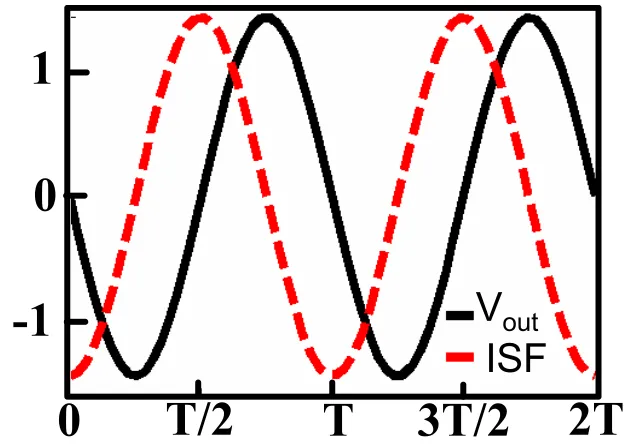
As an example, Figure 2.13 shows the ISF with a dashed red line together with the
output voltage waveform with a solid black line, of a typical LC oscillator. As can be seen,
there are regions on the oscillation cycle where the oscillator is more sensitive and less
sensitive to perturbations
In practice, an active device creates an energy restoring mechanism to compensate for
the losses of the tank and thus sustain the oscillation. This device acts as a means to
transfer the energy from the dc power supply to the resonant tank. Unfortunately, during
this energy transfer process, the active device also injects noise into the tank, which in turn
becomes phase noise.
Γ ω( )t
[image:38.612.119.433.164.386.2]α ω( )t
Figure 2.13: ISF and output voltage waveforms of a typical LC oscillator.
V
outISF
0
-1
1
0
1
-1
2.4. Oscillator Phase Noise 21
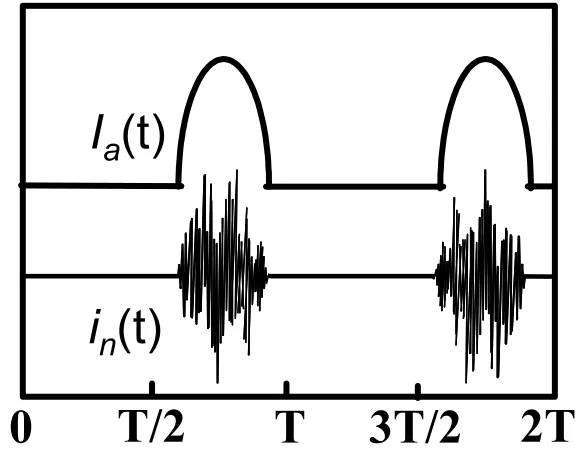
As another example, Figure 2.14 shows the drain current and a sample of the channel
noise in a MOS transistor.
These two effects combined are captured by the effective ISF, which is the product of
the ISF and the NMF. The NMF describes the noise amplitude modulation of the active
sources, which are the dominant factor in degrading the oscillator’s phase noise [22][24].
The relative timing of the cyclostationary noise sources with respect to the ISF can
drastically change the effect of these noise sources; therefore, it is highly desirable for the
cyclostationary noise sources to have their maximum power at the minimum sensitivity
point. In essence, (2.16) states quantitatively the way the phase noise is affected by these
processes.
As previously discussed, active device noise (and not the resonator noise) dominates
the phase noise of most CMOS oscillators. In a properly designed oscillator, the quality
factor, Q, of the resonant tank plays a central role in the phase noise, indirectly. The best
I
a
(t)
[image:39.612.180.468.145.370.2]i
n
(t)
Figure 2.14: Drain current and a sample of the channel noise in a MOS transistor.
phase-noise-power trade-off is usually achieved at the borderline between the current and
voltage limited regimes [24][25]. These two regions are depicted in Figure 2.15.
For sufficiently large bias currents, the oscillator tank voltage starts to clip due to the
inability to grow beyond the supply voltage, and thus the tank amplitude reaches a plateau.
On the other hand, the tank amplitude is proportional to at the current limited
regime (and also at the edge of the voltage-limited regime), where is the oscillator
dc bias current and is the equivalent tank parallel resistance [25]. A higher tank Q
translates to a larger effective tank parallel resistance, . This, in turn, allows the
designer to lower the oscillator’s bias current, , while maintaining the full voltage
swing necessary for operation at the edge of the voltage-limited regime. The lower bias
current decreases the noise from the active devices, which is the dominant contributor to
phase noise. This explains the well-established fact that higher tank quality factor can be
[image:40.612.109.454.157.382.2]used to improve oscillator phase noise.
Figure 2.15: Oscillator tank voltage vs. bias current of a typical LC oscillator.
0 0.5 1 1.5 2 2.5 3
0 5 10 15 20
Tail Current [mA]
Tank Voltage Swing [V]
Current Limited
Voltage Limited
Ibias⋅Rtank
Ibias
Rtank
Rtank
2.5. Challenges in Integrated Oscillator Design 23
2.5
Challenges in Integrated Oscillator Design
There are several issues in the design of local oscillators in CMOS technologies.
Firstly, the transistor devices readily available in these process technologies generate more
active device noise due to short channel and hot electron effects [9], hence suffering from
a worse phase noise performance than oscillator modules fabricated using discrete
components. Moreover, the 1/f noise corner in these devices is quite high, on the order of
hundreds of kilohertz to several megahertz for sub-micron silicon technologies, posing
another challenge for low noise oscillator design due to the up-conversion of this noise to
close-in phase noise around the carrier. Secondly, as the driving force in CMOS
technologies are digital applications, these technologies are not optimized for analog or
RF applications. Furthermore, to avoid latch up of the digital circuits, the silicon substrate
is fairly conductive and increases the signal loss because of the energy coupled (both,
inductively and capacitivelly) into the lossy substrate. Therefore, the quality factors of the
passive components available are quite low. Integrated capacitors present low capacitance
densities and large bottom plate capacitances that would degrade their RF performance
and worsen their effective loss. In addition, on-chip inductors suffer from high ohmic
losses from the thin metal layers available in CMOS technologies. This is exacerbated by
the skin effect, which causes a non-uniform current distribution in a conductor at high
frequencies. The consequence is a reduction in the effective inductor cross-section,
decreasing the metal conductance and hence, increasing the loss. What is more, due to the
proximity to the substrate, there will be energy coupled in to the substrate degrading the
inductor quality factor significantly.
2.6
Summary
Local oscillators are an essential building block in modern communications systems.
however, the far-out phase noise is determined by the spectral purity of the voltage
controlled oscillator and ultimately impacts the performance for such communication
systems. There are several challenges in oscillator design towards their integration in
silicon technologies, namely active device noise generation and low quality passives. We
will propose new architectures and topologies to overcome such issues in the following
Chapter
3
25
A Noise Shifting
Colpitts VCO
Integrated voltage controlled oscillators (VCOs) are essential building elements of all kinds of communication systems in general, and in particular, for the implementation of a single chip radio in today’s communication systems. The ever-growing demand for higher numbers of channels keeps imposing tighter phase noise performance specifications for local oscillators.
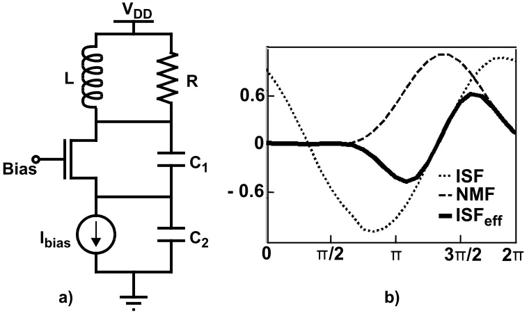
Recently, many different approaches have been used to improve the performance of integrated LC VCOs [24]-[49]. Cross-coupled oscillators have been preferred over other topologies due to their ease of implementation, relaxed start-up condition, and differential operation. However, in cross-coupled oscillators the noise generation by the active devices occurs when the oscillator is quite sensitive to perturbations [22] degrading the phase noise considerably. On the other hand, the Colpitts oscillator [31][40] has superior cyclostationary noise properties and can hence potentially achieve lower phase noise [50]. Despite these advantages, single-ended Colpitts oscillators are rarely used in today’s integrated circuits due to their higher required gain for reliable start-up and single-ended nature that makes them more sensitive to parameter variations and common-mode noise sources, such as substrate and supply noise.
3.1
Oscillator Topology Comparison
In this section, several oscillator topologies will be compared with an emphasis on their cyclostationary noise properties and energy transfer efficiencies to obtain essential understanding of their effect on the oscillator’s phase noise. This comparison is carried out in the context of the oscillator impulse sensitivity and noise modulating functions introduced in Section 2.4.
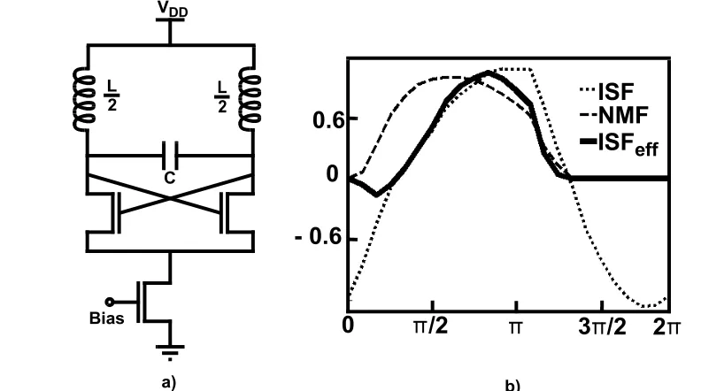
[image:44.612.92.488.250.471.2]Figure 3.1a shows the NMOS-only cross-coupled oscillator topology, widely used in high-frequency integrated circuits due to the ease of implementation and differential operation. Figure 3.2a shows the complementary version using both NMOS and PMOS transistors. This topology provides a larger tank amplitude for a given tail current in the current limited regime [25]. Finally, Figure 3.3a depicts the single-ended Colpitts oscillator topology, which is a commonly used in single-ended design [31][51][52]. Figure 3.1: NMOS-only cross-coupled oscillator: a) Circuit schematic, b) ISF, NMF and
effective ISF waveforms. VDD
Bias C L
2
ISF
NMF
ISF
effL 2
0
0.6
- 0.6
a) b)
3.1. Oscillator Topology Comparison 27
Figure 3.2: Complementary cross-coupled oscillator: a) Circuit schematic, b) ISF, NMF and effective ISF waveforms.
VDD
Bias C
L
ISF
NMF
ISF
eff0
0.8
- 0.4
0.4
a) b)
0
/2
3
/2 2
VDD
C1 L
C2 R
Bias
Ibias
ISF NMF
ISFeff
a) b)
0 0.6
- 0.6
0 /2 3 /2 2
[image:45.612.129.509.433.660.2]To simulate the ISF and NMF waveforms of the abovementioned oscillators, the direct impulse response measurement method of [22] is implemented in Spice [53]. In order to compare these oscillator topologies, these three oscillators are simulated using the same tank inductance and are tuned to oscillate at a center frequency of 1.8GHz, while maintaining a tuning range of at least 20%. The inductors have a quality factor of 5 at 1.8GHz. Finally, the oscillators draw the same bias current and operate in the current limited regime.
Figure 3.1b shows the simulated impulse sensitivity function, , noise modulating function, , and the effective impulse sensitivity function, , of the NMOS transistor channel noise in the NMOS-only cross-coupled topology of Figure 3.1a. In this oscillator topology, the maximum noise generated by the active devices appears when the oscillator is quite sensitive to perturbations. This can be noticed in Figure 3.1b, where the maximums of the NMF and ISF almost overlap, resulting in a large effective ISF and thus worsening the phase noise for a given resonator quality factor and bias current.
Figure 3.2b shows the simulated waveforms for the PMOS transistors in the complementary cross-coupled oscillator of Figure 3.2a. The waveforms of the NMOS transistors are comparable and are omitted without loss of generality. Similar to the NMOS-only cross-coupled topology discussed previously, the noise generated by the active devices of the complementary cross-coupled oscillator of Figure 3.2a is maximum when the oscillator’s phase is quite sensitive to perturbations. Moreover, in this topology the noise generated by both PMOS and NMOS transistors add to the overall active noise of the oscillator. Nevertheless, the complementary cross-coupled oscillator shows a better phase noise performance when compared to the NMOS- or PMOS-only cross-coupled oscillators for the same supply voltage and bias current when operating at the current limited regime, as demonstrated experimentally in [25]. This is mainly because the complementary cross-coupled oscillator of Figure 3.2a presents a larger maximum charge
Γ ω( )t
3.1. Oscillator Topology Comparison 29
swing, , than that of the NMOS- or PMOS-only cross-coupled oscillators which overall enhances its phase noise performance, as will be discussed shortly. In these two oscillator topologies, each of the cross-coupled transistors operate fully switching over half of the oscillation period. Thus, in the ideal case, their noise modulating function would be a square wave. However, these transistors require some time to switch completely and hence, show noise modulating functions depicted in Figure 3.1b and Figure 3.2b. In other words, the noise generation in these cross-coupled oscillator topologies occurs over the entire oscillation cycle, worsening their phase noise performance for a given resonator quality factor and bias current.
It is instructive to compare the contributions of each of the noise sources to the total phase noise in the complementary cross-coupled topology of Figure 3.2a. Table 3.1 shows the simulated phase noise contributions of different noise sources at 600KHz offset from a 1.8GHz carrier of the cross-coupled oscillator depicted in Figure 3.2a. It can be clearly seen that most of the circuit noise is generated by the drain current noise of the cross-connected transistors, while the combined contributions of the other noise sources accounts for less than 13% of the total phase noise power. For example, if the noise injected by the tail device could be completely removed, the total phase noise would only show an improvement of 0.22 dB in this oscillator.
On the other hand, the single-ended Colpitts oscillator of Figure 3.3a has better cyclostationary noise properties, as exhibited in the simulated , , and
waveforms depicted in Figure 3.3b. In this topology, the maximum noise
Noise Source Contribution
Drain current 87%
Inductor 6%
Tail Current 5%
Varactor 2%
Table 3.1: Phase noise contribution of each noise source.
qmax
Γ ω( ) α ωt ( )t
generation instant is aligned with the oscillator’s minimum sensitivity point and can hence potentially achieve lower phase noise. Also, the Colpitts oscillator presents a smaller rms and dc value of its effective ISF than that of the NMOS- or PMOS-only and complementary cross-coupled oscillators of Figure 3.1a and Figure 3.2a, respectively. A more symmetrical effective ISF will significantly reduce the up-conversion of the low frequency noise of the transistor [22]. It is noteworthy that in the single-ended Colpitts oscillator of Figure 3.3a, the conduction angle of the main transistor is determined by the ratio, and thus it is highly desirable to minimize this conduction time. In practice, this conduction time has an optimum when this ratio is about 4 [54]. Fortunately, in this oscillator topology, the maximum of the core transistor current conduction (or the maximum of the noise power generation) occurs at the oscillator minimum sensitivity point.
As previously discussed, while the better cyclostationary properties of an oscillator alone would enhance the phase noise performance, a large oscillation charge swing results in an increase in the tank stored energy. The tank energy Etank in an oscillator is given by , where Vtank is the tank voltage amplitude. Moreover, if the oscillator operates in the current limited regime, Vtank can be expressed in terms of the bias current
Ibias and the effective parallel tank resistance Rtank, i.e.,
(3.1)
where β is the oscillation amplitude constant. The energy transfer efficiency, , which is defined as the ratio of the energy stored in the resonator’s tank Etank to the total dc energy
Pdc dissipated in one period can be expressed as:
C2⁄C1
Etank = CVtank2 ⁄2
Vtank = βRtankIbias
3.1. Oscillator Topology Comparison 31
(3.2) where is the oscillation period and Vdc is the supply voltage. Also, it is assumed that the quality factor of the tank is given by .
Equation (3.2) shows the well-established fact that increasing the tank’s quality factor will improve the energy transfer efficiency and enhance the phase noise of the oscillator. However, this energy transfer efficiency can also be increased if the oscillator has a larger oscillation amplitude for a given bias current (i.e., larger β). To illustrate this, Table 3.2 compares the oscillation amplitude constant β for the NMOS- and PMOS-only, complementary cross-coupled and Colpitts VCOs of Figure 3.1a, Figure 3.2a, and Figure 3.3a, respectively.
It can be easily seen that the Colpitts oscillator presents a higher output voltage swing and higher energy transfer efficiency than that of the NMOS- or PMOS-only and
Oscillator Amplitude Oscillation amplitude constant, β
Energy transfer efficiency, η NMOS- or PMOS-only cross-coupled Complementary cross-coupled Single-ended Colpitts
Table 3.2: Oscillator comparison.
η Etank
PdcT
---=
CVtank2 fosc
2VdcIbias
---=
Qtank2 β2Ibias
4πVdc
--- L C ----⋅ = T 1 fosc
--- 2π LC
= =
Q = Rtank⁄2πfoscL
2 π
---RtankIbias 2⁄π 1
π2
--- Qtank
2 I
bias L C⁄
πVdc
---⋅
4 π
---RtankIbias 4⁄π 4
π2
--- Qtank
2 I
bias L C⁄
πVdc
---⋅
2RtankIbias 2 1 Qtank2 Ibias L C⁄ πVdc
complementary cross-coupled oscillators for a given bias current, which will further enhance its phase noise. It is also noteworthy that the efficiency is proportional only to the square-root of the L/C ratio. Interestingly, in the case of integrated spiral inductors, reducing the L results in a stronger improvement in the Q2 term compared to the , as discussed in more details in [24].
Despite these advantages, single-ended Colpitts oscillators are rarely used in today integrated circuits, due to the higher required gain for reliable start-up and their single-ended nature that makes them more susceptible to common-mode noise sources such as substrate and supply noise. In the following section we will present a new topology that remedies these problems. Most of the discussed properties of the single-ended Colpitts oscillator of Figure 3.3a are applicable to the oscillator topology presented next.
3.2
Design Evolution
In this section, starting from the single-ended Colpitts oscillator of Figure 3.3a, we will show the design evolution that leads to a topology that overcomes the start-up issues while providing a low-noise fully-differential output.
A differential output can be provided by coupling two identical Colpit