2016 International Conference on Mathematical, Computational and Statistical Sciences and Engineering (MCSSE 2016) ISBN: 978-1-60595-396-0
Design of High Stability LDO Based on CMOS Technology
Dan BU, Mei-hong LI, Si-qi LI and Cheng-jun QIU
*130#, Key laboratory of electronics engineering of Heilongjiang province, Heilongjiang University, Harbin, China
*Corresponding author
Keywords: Linear regulator, Low dropout, High stability.
Abstract. This paper presents a low dropout linear regulator (LDO) structure designed by 0.18um CMOS process; it includes the bandgap voltage reference with good temperature characteristic, the error amplifier of high gain and good PSRR, the power adjustment transistor and resistance feedback network which have reasonable sizes, and slew rate enhancement circuit. The circuit simulation and layout design are successfully completed. The experimental results of LDO show that the circuit gain is 99.47dB, the phase margin is 67.27°, and the PSRR is 90.65dB. The linear adjustment rate is 0.3%, the load adjustment rate is 2.7%; the quiescent current is 56.1uA, the temperature drift coefficient is 8.04ppm/°C, and the layout area is 0.04mm2. This design meets the requirements that are low dropout, high stability and small area.
Introduction
The low dropout linear regulator is a power management chip which provides a stable output voltage; it will generate a stable and high precision output voltage in a wide range of load current [1]. When the requirement of output current is less, the cost of LDO is lower, the peripheral circuit is simple, the occupied area is small; to compared with other power, its output voltage ripple and output voltage noise are very low, and there is no electromagnetic interference caused by the large current changes in the clearance of the switch [2].
Principle and Structure
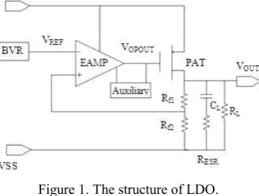
[image:1.595.207.390.592.730.2]The structure of LDO is shown in Figure 1, it includes bandgap voltage reference, current reference, error amplifier, power adjustment transistor, resistance feedback network, and slew rate enhancement circuit, and the auxiliary circuit should be added to protect the whole circuit [3, 4]. The core of LDO is the error amplifier and the power adjustment transistor; they constitute a negative feedback closed loop system through the resistive negative feedback network.
Figure 1. The structure of LDO.
adjustment transistor, which can adjust the output current tracking load and make the output of LDO stable [5].
Bandgap Voltage Reference
The structure of bandgap voltage reference is shown in Figure 2. In order to provide a stable reference voltage, it needs to have good temperature characteristics, the ability to suppress the ripple and low noise; the simulation results show that the output voltage is stable, as 1.25V, the voltage change is 2.5mv when the temperature changes in the range of -45°~80°. The temperature coefficient is about 20ppm/°C, PSRR is 73.04dB, and the total output noise is only 60.62uV. Thus, the bandgap voltage reference circuit meets the design requirements.
[image:2.595.106.497.215.374.2]
Figure 2. The bandgap voltage reference. Figure 3. The error amplifier circuit.
Error Amplifier
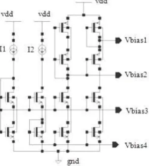
The error amplifier is the most important modules of LDO, its quality is closely related with the many important characteristic indexes of LDO, such as output voltage precision, load current, leakage voltage and so on [6]. The error amplifier circuit needs four bias voltages in Figure 3; the bias circuit as shown in Figure 4 provides the required bias voltages that are 1.166V, 1.672V, 1.404V, 1.06V, successively. The bias current circuit provides 10uA reference current as shown in Figure 5.
The simulation results of error amplifier are shown that its gain is 105.5dB, phase margin is 60.7°, unit gain bandwidth is 7.449MHz; SR is 204 V/us, the response rate is fast; CMRR and PSRR are 83.39dB and 84.63dB respectively, the common mode rejection and ripple rejection ability are better.
[image:2.595.102.253.543.711.2] [image:2.595.280.498.555.710.2]
Figure 4. The bias voltage circuit. Figure 5. The current reference circuit.
Slew Rate Enhancement Circuit
time of power tube and produced larger overshoot voltage. These results are undesirable, thus the slew rate enhancement circuit is designed to solve the problem, as shown in Figure 6, which consists of a comparator and a PMOS transistor.
[image:3.595.65.293.129.278.2] [image:3.595.305.521.508.669.2]
Figure 6. The slew rate enhancement circuit. Figure 7. The load adjustment rate.
Simulation and Layout of LDO
Load Regulation Rate
The input voltage is constant; the output voltage will change with the load current fluctuations. As shown in Figure 7, the change value of the output voltage is about 8mV, the load adjustment rate is 2.7% by calculated, and the variation of load has little effect on the output voltage.
Linear Adjustment Rate
When the load current is constant, the output voltage changes with the input voltage, the variation of the output voltage is 9mv as shown in Figure 8. The linear adjustment rate is 0.3% by calculated. When the input voltage is 2V, the output voltage keeps stable at 1.8V, the difference between input and output voltage is about 200mv.
Figure 8. The linear adjustment rate. Figure 9. The temperature characteristic curve.
Temperature Characteristic
Stability and PSRR
PSRR represents the stability of the whole circuit system; it describes that how the output signals to inhibit the small scale fluctuations of supply voltage. The simulation result is shown in Figure 10, PSRR is 90.65dB. In addition, through the analysis of amplitude frequency response and phase frequency response, the gain of the circuit reaches 99.47 dB and the phase margin is 67.27°, as shown in Figure 11.
[image:4.595.92.513.177.317.2]
Figure 10. The simulation result of PSRR. Figure 11. The frequency response analysis.
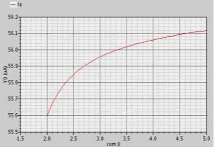
Quiescent Current
The overall power consumption of LDO is determined directly by quiescent current, the quiescent current consumed by circuit is shown in Figure 12, the maximum quiescent current is 56.1uA, the minimum is 55.6uA, it has lower power consumption and very high conversion efficiency.
Layout Design
The layout design of LDO is shown in Figure 13, which includes bandgap voltage reference, current reference, error amplifier, power adjustment transistor, resistance feedback network, and slew rate enhancement circuit, the area is about 0.04mm2.
[image:4.595.189.408.491.642.2]
Figure 13. The layout design of LDO.
Comparison and Discussion
To compare with the other three papers in Table 1 [7,8,9], the comparison results are shown that the input voltage range and the load current designed in this paper are superior to the other three papers; The PSRR and layout area are better than the others. In general, the LDO designed in this paper has the characteristics, such as low dropout, high stability and small layout area.
Table 1. The comparison of LDO parameters.
Parameters ZH.H.ZH X. Junze L. Ch. Y. Design
Area [mm2] 0.043 0.045 0.065 0.04
PSRR [dB] 43 90 45 90.65
Technology [um] 0.18 0.18 0.18 0.18
Load regulation 2.6% 0.5% 11.5% 2.7%
Load current [mA] 0-120 0-100 0-50 0-300
Input voltage [V] 1-4 2.5-4 3-4 2-5
Output voltage [V] 1.8 1.7-1.8 2.9 1.8
Quiescent current [uA] 60 3.5 51.54 56.1
Linear adjustment rate 0.42% 0.1% 0.28% 0.3%
Conclusions
The principle and structure of LDO are studied in this project, and a high stability LDO is designed and simulated successfully. To compare with the related designs as the same technology level, the simulation results show that the LDO circuit we designed has the characteristics, such as high stability, low power consumption, high conversion efficiency, and good temperature characteristic, which meet the design requirements. In the future, the design will be finally verified and taped out.
Acknowledgement
This project was funded by the 2008 Heilongjiang University Youth Science Foundation Project (QL200808), and the Heilongjiang Provincial Education Department Key Laboratory Scientific Research Project of Electronic Engineering (DZZD20100034).
References
[1] Gabriel A., Analog IC Design of LDO, Science Press, Beijing, 2012.
[2] W. Qin, Research of low drop-out voltage regulator, Fudan University, Shanghai, 2012.
[image:5.595.137.461.353.501.2][4] X. Hua, Desgin of low drop-out regulator with low voltage, Xiamen University, Xiamen, 2009.
[5] Zh. Haobo, H. Yonggui, L. Siying, etc., Design of a very low dropout voltage linear regulator, Microelectronics. 43(2013) 186-198.
[6] F You, SHK Embabi, Multistage amplifier topologies with nested gm-C compensation, IEEE Solid State Circuit. 32(2007) 2000-2011.
[7] Zh. Hanzhong, Research and implementation of cap-free LDO, XiDian University, Xian, 2014.
[8] X. Junze, A low noise, fast transient response LDO, XiDian University, Xian, 2014.