© 2016, IRJET | Impact Factor value: 4.45 | ISO 9001:2008 Certified Journal
| Page 1360
Reconfigurable C and Ku band antenna Using Duelpatch
Anil John pulickapunathil
1, Mr.S. Parameswaran
21
ME, Nandha College of Technology, Tamilnadu, India.
2
Asst Professor – ECE,
Nandha College of Technology, Tamilnadu, India
---***---Abstract -
- A reconfigurable C and Ku band patch antenna with C-Slot and dual-patch elements is proposed and studied. It occupies a compact volume of 80× 60× 1.57mm, including the ground plane. The antenna can operate in 4,5,10 and 12 GHz bands. Two C-Slots on the patch elements are employed to perturb the surface current paths for excitation of the dual-band modes. Two switches, implemented using PIN diodes, are placed on the connecting lines of a simple feed network to the patch elements. Different set of frequencies are achieved by switching “ON” either one of the two patch elements. The frequencies in the dual-band modes can be independently controlled using positions and dimensions of the C-Slots. The advantage of the proposed antenna is that two dual-band operations can be achieved using the same dimensions. This overcomes the need for increasing the surface area normally incurred when designing wideband patch antennas. Simulations are done in HFSS v.9.Key Words: WLAN, WiMAX, PEC, UWB, FR4 epoxy, MEMS switches, PIN diodes, C-shaped patch.
1.INTRODUCTION
With the ever-increasing need for mobile communication and the emergence of many systems, it is important to design broadband antennas to cover a wide frequency range. The design of an efficient wide band small size antenna, for recent wireless applications, is a major challenge. Microstrip patch antennas have found extensive application in wireless communication system owing to their advantages such as low-profile, conformability, low-cost fabrication and ease of integration with feed networks [1]. However, conventional microstrip patch antenna suffers from very narrow bandwidth, typically about 5% bandwidth with respect to the center frequency. This poses a design challenge for the microstrip antenna designer to meet the broadband techniques [2]-[3]. There are numerous and well-known methods to increase the bandwidth of antennas, including increase of the substrate thickness, the use of a low
dielectric substrate, the use of a range of impedance matching and feeding techniques, the use of multiple
resonators, and the use of slot antenna geometry [4]-[5]. However, the bandwidth and the size of an antenna are generally mutually conflicting property, that is, improvement of one of the characteristics normally results in degradation of the other. Recently, several techniques have been planned to enhance the bandwidth. A novel single layer wide-band rectangular patch antenna with attainable impedance bandwidth of greater than 20% has been demonstrated [6]. Utilizing the shorting pins or shorting walls on the uneven arms of a U-shaped patch, U-slot patch, or L-probe feed patch antennas, wideband and the dual-band impedance bandwidth have been achieved with electrically small size [7]. Other techniques involves employing multilayer patch structures with parasitic patches of a range of geometries such as E, V and H shapes, which excites multiple resonant modes. On the other hand, these antennas are commonly fabricated on thicker substrates and are large in sizes and difficult to fit into small and slim devices.
© 2016, IRJET | Impact Factor value: 4.45 | ISO 9001:2008 Certified Journal
| Page 1361
the need for using two ports as proposed in [10] and increases the number of possible frequency bands from one to six.
2.ANTENNA DESIGN
A. Patch design
(1)
(2)
(3)
(4)
(5)
Where W is width, L is length, h is height of substrate.
B. Design of slot
1) Use the equations for width and length of patch for the desired frequency
2) The position of the slot can be approximately the length from the patch.
3) With trial and error method, using nearby values for width and length fix the position and length of the slot.
4) Only larger frequencies can be included in the patch designed for lower frequency.
3. DUAL FREQUENCY SLOT ANTENNA
With a single patch we can operate it in single frequency only. So there is a need for a technique for including another frequency in the same patch. By this the single patch can work in two set of frequencies. Slot technique enables the patch to work in two set of frequencies. Making a slot is a simple technique that it does not increase the size.
In this paper, the desired frequencies are 3 and 10 GHz. These frequencies are used for satellite TV communication. Aim is to design an antenna which can work in both the frequencies.
[image:2.595.303.566.173.418.2]The dimensions for the 3 GHz patch are designed using the design equations. Using these dimensions a patch is made. Then the dimensions for 10 GHz patch are obtained. These dimensions are set as slot dimensions. Using these dimensions.
Fig – 1: Top view of dual frequency slot antenna
slots are to be made. Various positions for the slot has to be tried on the patch with above obtained dimensions
3.1 Structure
© 2016, IRJET | Impact Factor value: 4.45 | ISO 9001:2008 Certified Journal
| Page 1362
epoxy with dielectric constant of 4.4 and tangent loss of 0.003 is used. Generally, substrate materials can be separated into three categories according to the dielectric constant εr.
1) Having a relative dielectric constant εr in the range
of 1.0–2.0. This type of material can be air, polystyrene foam, or dielectric honeycomb.
TABLE 1:DIMENSIONS OF DUAL FREQUENCY ANTENNA
A B C D E F G H
10 12 28 9 2 30 50 50
2) Having εr in the range between 2.0–4.0 with
material consisting mostly of fiberglass reinforced Teflon.
3) With εr between 4 to 10. The material can consist of
quartz, or alumina, ceramic.
The feed point is of 50Ω. The feed network is designed such that there is impedance matching between feed and the patch. Practically it is 30 % larger than the conducting patch. In between ground plane and conducting sheet there is substrate material which is a dielectric with εr = 4.4.
3.2 Patch
Patch is the radiating part in the antenna. It is designed for a particular frequency known as resonant frequency. The material used for patch in this project is PEC which has the properties of perfect conductor. The dimension of patch determines the resonant frequency.
3.3 Substrate
Width of the substrate h has a big effect on the resonant frequency and bandwidth of the antenna. Bandwidth of the microstrip patch antenna will increase with increasing of substrate width h but with limits, otherwise the antenna will stop resonating.
3.4 Feeding techniques
Because of the antenna is radiating from one side of the substrate, so it is easy to supply it from the other side (the ground plane), or from the side of the element. The most important thing to be measured is the maximum transfer of
power (matching of the feed line with the input impedance of the antenna).
In this paper, microstrip feed line is used. Here there is microstrip feed line to which signal is fed. It is on the side of the substrate between patch and ground plane. The impedance of the feed line is 50Ω. Between patch and feed line there is feed strip whose impedance should be matched with patch so that maximum power transfer occurs and the reflection is minimum.
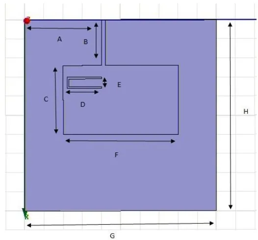
[image:3.595.306.566.244.482.2]4. RECONFIGURABLE C AND KU BAND ANTENNA
Fig – 2: Top view of reconfigurable antenna
TABLE II:DIMENSIONS OF RECONFIGURABLE ANTENNA
A B C D E F G H I J
22 9.6 27 9 2 9 30 35 30 22
K L M N O P
7 8 4 9 80 60
4.1 Design
© 2016, IRJET | Impact Factor value: 4.45 | ISO 9001:2008 Certified Journal
| Page 1363
design equations given in chapter 2 for 4 and 5 GHz. Then slot dimensions are obtained. The slot position is fixed by trying different values. The feed network is known as corporate feed. The feed has to be designed in such a way that impedance matching has to be obeyed between patch and the feed. We have three modes of operation by making the diodes ON and OFF. The three modes are ON-OFF, OFF-ON and OFF-ON-OFF-ON. By this we get different set of operating frequencies which make the design reconfigurable.
5. DISCUSSION
5.1 S11 of dual frequency patch
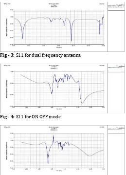
[image:4.595.307.566.83.206.2]In fig. 3 we can notice that there are two set of -10 dB bandwidth in 3 to 3.5 GHz and 9.5 to 10 GHz. Both have 500 MHz bandwidth. We obtained two set of frequencies using slot.
Fig - 3: S11 for dual frequency antenna
Fig - 4: S11 for ON OFF mode
Fig – 5: S11 for OFF ON mode
Fig - 6: S11 for ON ON mode
Without the slot the antenna will only have -10 dB bandwidth at 3 GHz. Thus we were able to obtain dual frequency using a single patch.
5.2 S11 of C and Ku band antenna
Here we have to examine three plots. The plots are fig. 4, fig. 5 and fig. 6. In the first figure we can notice -10 dB bandwidth at 5.5 to 6 GHz and 10 to 11 GHz. We have 500 MHz bandwidth in first set and 1 GHz bandwidth in the second set. In the second figure we have -10 dB bandwidths at 5 to 5.5 GHz and 11 to 12 GHz. So in total we have achieved 5 to 6 GHz and 10 to 12 GHz. These set can be used for satellite TV reception. In the third figure we have -10 dB bandwidths at 5 and 7 GHz having 500 MHz bandwidth each. These set can be used for WLAN applications.
The plots have several irregularities. There are many peaks and dips in the plot which are undesired. These are due to impedance mismatch between feed at the patch. If we examine the current distribution, we can notice currents in the patch which is OFF. This is due to mutual coupling between the patches.
5.3 Design hindrances
The equations given are approximate equations. So we will have to try many values to get the required result.
The feeding strip has to be matched with feed at patch impedances. This makes the design tough.
The slot dimensions are in millimeter which makes the manufacturing difficult. As the frequency increases the size decreases which demands manufacturing with high degree of precision.
5.4 Problems
1) Impedance matching
The feed strip should be matched with source and patch. This design should be done with atmost care.
[image:4.595.36.295.364.722.2]© 2016, IRJET | Impact Factor value: 4.45 | ISO 9001:2008 Certified Journal
| Page 1364
As the distance between patches is small mutual coupling will occur. This will result in unwanted -10 dB frequencies in S11 plot.
5.5 Applications
C band receiver, Ku band receiver and WLAN antenna
6. FUTURE SCOPE
1) Include frequency sets 4-5 GHz and 12-14 GHz for complete C and Ku band
2) Proper design to avoid impedance mismatch
3) Place proper material to avoid mutual coupling
4) Good dielectric material to avoid spurious radiation
5) Apt design which will reduce size and increase gain simultaneously
REFERENCES
[1] He W., Jin R., Geng J., “E-Shape patch with wideband and circular polarization for millimeter-wave communication”, IEEE Transactions on Antennas and Propagation, vol.56, issue 3, pp.893-895, 2008.
[2] Lau K.L., Luk K.M., Lee K.L., “Design of a circularly-polarized vertical patch antenna”, IEEE Transactions on Antennas and Propagation, vol.54, issue 4, pp.1332- 1335, 2006.
[3] Zhang Y.P., Wang J.J.,“Theory and analysis of differentially-driven microstrip antennas”, IEEE Transactions on Antennas and Propagation, vol.54, issue 4, pp.1092-1099, 2006.
[4] M. Pozar, “Microsrtip Antennas”, Proceedings of IEEE, vol.8, No.1, January 1992.
[5] Wi. S. H. et al, “Package-Level integrated antennas based on LTCC technology”, IEEE Transactions on Antennas and Propagation, vol.54(8), pp.2190–2197, 2006.