2018 International Conference on Information, Electronic and Communication Engineering (IECE 2018) ISBN: 978-1-60595-585-8
Improvement of Corrosion Process for Gate Commutated
Thyristor Chips
Wen-peng ZHOU
*, Rong ZENG, Zhan-qing YU, Jia-peng LIU, Wei-jia YANG,
Gang LYU and Chao-qun XU
Department of Electrical Engineering, Tsinghua University, Beijing, China
*Corresponding author
Keywords: GCT chip, Corrosion process, Process sequence, Process operation.
Abstract. In recent years, with the continuous development of installed grid capacity and renewable energy, DC power transmission and distribution technologies have developed rapidly. As one of the most important high power semiconductor devices, the integrated gate commutated thyristor (IGCT) has great potential in DC grid application. The gate-cathode blocking property is the key for device packaging and working. Based on the corrosion process of the GCT chip, two methods are proposed for improving the consistency of gate-cathode blocking voltage in this paper.
Introduction
With fast growing power generation capacity and evolving clean energy, DC transmission and distribution technologies have developed rapidly recent years, due to advantages such as large transport capacity, extra long-distance transportation and lower loss. Integrated gate commutated thyristor (IGCT) is a kind of fully controlled power electronic device and its excellent blocking voltage and high current turn-off capability make it suitable for high-capacity applications such as DC breakers[1, 2] and SVCs, etc. However, there are many important factors influencing the usage of IGCT, the properties between gate and cathode is one of them.
This paper analyzes and discusses the corrosion process of the GCT chip part of IGCT, and proposes two corrective methods from the aspects of process sequence and process operation based on process and device simulation results.
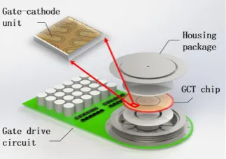
[image:1.595.217.379.625.739.2]Process Introduction of Gate-Cathode Units
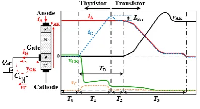
Figure 1 shows the schematic of the integrated gate commutated thyristor (IGCT), which consists of the GCT chip, the housing package and the gate drive circuit. The turn-off process of IGCT is shown in Figure 2[3], through the instant applied reverse voltage provided by the gate driver between gate and cathode, the cathode current is transferred to the gate. After this transformation, the device changes into an open-gate PNP transistor and turns off the current gradually.
voltage than the given voltage will cause the whole device’s failure. However, if there’s any PN junction with a too high blocking voltage, then the doping around this area will do harm to the current commutation process[4]. As a result, it’s important to keep the consistency of the PN junction units throughout the device through fabrication process.
Figure 2. The turn-off process of an IGCT[3] .
The structure diagram of a single cathode unit of the GCT chip is described in Figure 3. A cathode unit is composed of the N+ emitter region, the P+ base region, the moat shape[5], and the passivation layer between gate and cathode. Both the N+ emitter region and the P+ base region are fabricated by conventional doping diffusion method. And the passivation layers are composed of silicon dioxide and organic layer. The moat shape is performed by wet etching process, which determines the withstand voltage of the PN junction together with the N+ emitter region and the P+ base region.
Early papers discussed the gate-cathode blocking property based on small-sized devices (mainly 2-inch ones) [6, 7], but these papers did not discuss it in detail from the aspect of the fabrication process. As the size of the wafer grows, the number of gate-cathode units on the device increases, changing from tens of hundreds (2-inch) to thousands or ten thousand (4-inch and 6-inch). So the discussion on the consistency of the gate-cathode blocking property of the device is becoming more and more important.
Figure 3. The schematic of a gate-cathode unit of a GCT chip.
[image:2.595.187.410.449.598.2]Figure 4. Comparison of doping profiles of gate-cathode units with different junction positions.
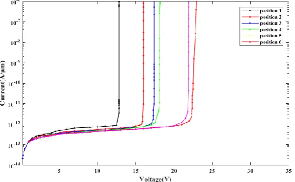
And the results are shown in Figure 5. When the PN junction is at different positions on the sidewall of the moat shape, the gate-cathode unit blocking voltage changes. And the changes are mainly decided by the P+ base region doping of junction below the sidewall surface. It should be noticed that when the position is near the bottom of the moat shape or at the bottom of the moat shape, the voltage changes little.
Figure 5. Comparison of blocking properties of gate-cathode units with different junction positions.
Usually there are two ways to realize the fabrication of gate-cathode units.
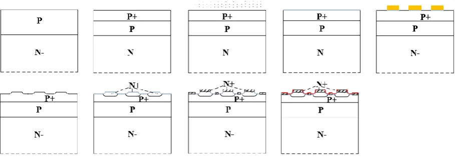
For process sequence 1, the N+ emitter region is firstly fabricated and then the moat shape is etched, so there are two steps of lithography processes. And more random errors will appear between the two steps, so the junction asymmetry of the gate-cathode unit is more likely to occur, which causes the blocking voltage to deviate from the design level. As a result, the consistency of the gate-cathode unit blocking voltage becomes worse.
[image:3.595.146.447.311.497.2]Figure 6. The first kind of process flow for making the gate-cathode units.
Figure 7. The second kind of process flow for making the gate-cathode units.
Optimization of the Corrosion Operation Process
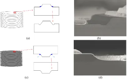
To make the moat shape, the traditional wet etching process is adopted. The main steps include the etching step in the etchant solution and the flushing step in the deionized water. After the etching step, it is necessary to transfer the wafers quickly into the deionized water for acid flushing to avoid extra local etching. However, not only the speed of transfer process but also the position of the wafers will cause extra local etching.
[image:4.595.71.526.272.431.2]
(a) (b)
[image:5.595.97.506.71.328.2]
(c) (d)
Figure 8. The comparison of different wafer positions during the corrosion process and the fabrication results. (a: the cathode side faces upwards; b: the SEM of the sample when the cathode side faces upwards; c: the anode side faces
upwards; d: the SEM of the sample when the anode side faces upwards)
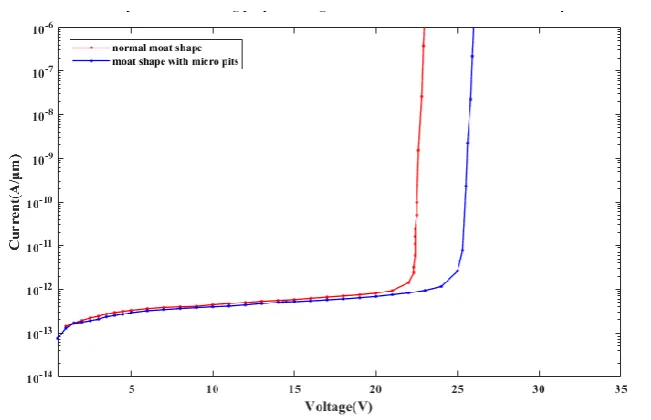
To study the influences of these micro pits at the corner, different shapes of the gate-cathode units are created by Athena in Silvaco based on the fabrication process parameters. And then the gate-cathode blocking property sweeping is made. When the junction is at the micro pits, it can be seen form the results that the gate-cathode units with micro pits have higher blocking voltage, which means the lower doping in the P+ base region below the surface. Because of the random of the micro pits and the junction positions, there will be different doping in the P+ base region, which will do harm to the current commutation process of IGCT. And the fabrication should try to avoid this situation.
[image:5.595.132.462.503.652.2]Figure 10. Comparison of doping of gate-cathode units with different moat shapes.
Conclusion
In this paper, the consistency of the blocking voltage of gate-cathode units on the GCT chip is studied. The asymmetry of the gate-cathode junction and the micro pits at the corner of the moat shape will affect the blocking voltage obviously. Based on these problems, two methods are brought up to improve the gate-cathode unit blocking voltage distribution.
Acknowledgement
This work was supported by the Science and Technology Project of State Grid Corporation under Grant SGZJ0000BGJS1600326.
References
[1] Novello L, Baldo F, Ferro A, et al. Development and testing of a 10-kA hybrid mechanical–static DC circuit breaker[J]. IEEE Transactions on Applied Superconductivity, 2011, 21(6): 3621-3627.
[2] Zhengyu Chen, Zhanqing Yu, Gang Lv, et al. Researches on 10 k V DC Hybrid Circuit Breaker Based on IGCT Series [J]. Proceedings of the CSEE, 2016, 36(2): 317-326.
[3] Chen Z, Yu Z, Liu X, et al. Stray Impedance Measurement and Improvement of high power IGCT Gate Driver Units[J]. IEEE Transactions on Power Electronics, 2018.
[4] Lyu G, Yu Z, Zeng R, et al. Optimisation of gate-commutated thyristors for hybrid DC breakers[J]. IET Power Electronics, 2017, 10(14): 2002-2009.