International Journal of Emerging Technology and Advanced Engineering
Website: www.ijetae.com (ISSN 2250-2459, Volume 2, Issue 6, June 2012)324
Design and Analysis of Low Power Full Adder Using
Adiabatic Technique
P.Sreenivasulu
1,
M.V.Narasimha reddy
2,
G.V.K. Varaprasad Swamy
3 1Asst. professor, Dept of E.C.E, Dr.S.G.I.T, Markapur, Prakasam (Dist),INDIA. 2Final Year, M.Tech Scholar (DECS), Dept of E.C.E,S.G.I.T, Markapur, INDIA.3Final Year, M.Tech Scholar(DECS), Dept of E.C.E,S.G.I.T, Markapur, INDIA. ,
Abstract –The energy stored at the output can be retrieved by the reversing the current source direction discharging process instead of dissipation in NMOS network. Hence adiabatic switching offers the less energy dissipation in PMOS network and reuse the stored energy in the output capacitance by reversing the current source direction. There are the many adiabatic logic design technique are given in Literature but here two of them are chosen ECRL and PFAL, which shows the good improvement in energy dissipation and are mostly used as reference in new logic families for less energy dissipation reduction of area & power factors the simulations were done using microwind & DSCH results
Index Terms— Adiabatic switching, energy dissipation, power clock, equivalent mode
I. INTRODUCTION
The main objective of this thesis is to provide new low power solutions for Very Large Scale Integration (VLSI) designers. Especially, this work focuses on the reduction of the power dissipation, which is showing an ever-increasing growth with the scaling down of the technologies. Various techniques at the different levels of the design process have been implemented to reduce the power dissipation at the circuit, architectural and system level. Furthermore, the number of gates per chip area is constantly increasing, while the gate switching energy does not decrease at the same rate, so the power dissipation rises and heat removal becomes more difficult and expensive. Then, to limit the power dissipation, Alternative solutions at each level of abstraction are proposed. The dynamic power requirement of CMOS circuits is rapidly becoming a major concern in the design of personal information systems and large computers. In this thesis work, a new CMOS logic family called
ADIABATIC LOGIC, based on the adiabatic switching principle is presented.
The term adiabatic comes from thermodynamics, used to describe a process in which there is no exchange of heat with the environment. The adiabatic logic structure dramatically reduces the power dissipation.
The Adiabatic switching technique can achieve very low power Dissipation, but at the expense of circuit complexity. Adiabatic logic offers a way to reuse the energy stored in the load capacitors rather than the traditional way of discharging the load capacitors to the ground and wasting this energy
This thesis work demonstrates the low power dissipation of Adiabatic Logic by presenting the results of designing various design/ cell units employing Adiabatic Logic circuit techniques. A family of full-custom conventional CMOS Logic and an Adiabatic Logic units for example, an inverter, a two-input NAND gate, a two-input NOR gate, a two-input XOR gate, a two-to-one multiplexer and a one-bit Full Adder were designed in Mentor Graphics IC Design Architect using standard TSMC 0.35 µm technology, laid out in Microwind IC Station.
All the circuit simulations has been done using various schematics of the structures and post-layout simulations are also being done after they all have been laid-out by considering all the basic design rules and by running the LVS program. Finally, the analysis of the average dynamic power dissipation with respect to the frequency and the load capacitance was done to show the amount of power dissipated by the two logic families.
II.MOTIVATION
In the past few decades ago, the electronics industry has been experiencing an unprecedented spurt in growth, thanks to the use of integrated circuits in computing, telecommunications and consumer electronics.
International Journal of Emerging Technology and Advanced Engineering
Website: www.ijetae.com (ISSN 2250-2459, Volume 2, Issue 6, June 2012)325
We have come a long way from the single transistor era in 1958 to the present day ULSI (Ultra Large Scale Integration) systems with more than 50 million transistors in a single chip [1].The ever-growing number of transistors integrated on a chip and the increasing transistor switching speed in recent decades has enabled great performance improvement in computer systems by several orders of magnitude. Unfortunately, such phenomenal performance improvements have been accompanied by an increase in power and energy dissipation of the systems. Higher power and energy dissipation in high performance systems require more expensive packaging and cooling technologies, increase cost, and decrease system reliability. Nonetheless, the level of on-chip integration and clock frequency will continue to grow with increasing performance demands, and the power and energy dissipation of high-performance systems will be a critical design constraint.
For example, high-end microprocessors in 2010 are predicted to employ billions of transistors at clock rates over 30GHz to achieve TIPS (Tera Instructions per seconds) performance [1]. With this rate, high-end microprocessor’s power dissipation is projected to reach thousands of Watts. This thesis investigates one of the major sources of the power/energy dissipation and proposes and evaluates the techniques to reduce the dissipation.
Digital CMOS integrated circuits have been the driving force behind VLSI for high performance computing and other applications, related to science and technology. The demand for digital CMOS integrated circuits will continue to increase in the near future, due to its important salient features like low power, reliable performance and improvements in the processing technology.
The word ADIABATIC comes from a Greek word that is used to describe thermodynamic processes that exchange no energy with the environment and therefore, no energy loss in the form of dissipated heat. In real-life computing, such ideal process cannot be achieved because of the presence of dissipative elements like resistances in a circuit. However, one can achieve very low energy dissipation by slowing down the speed of operation and only switching transistors under certain conditions. The signal energies stored in the circuit capacitances are recycled instead, of being dissipated as heat. The adiabatic logic is also known as ENERGY RECOVERY CMOS .
It should be noted that the fully adiabatic operation of the circuit is an ideal condition which may only be approached asymptotically as the switching process is slowed down. In most practical cases, the energy dissipation associated with a charge transfer event is usually composed of an adiabatic component and a non-adiabatic component. Therefore, reducing all the energy loss to zero may not possible, regardless of the switching speed. With the adiabatic switching approach, the circuit energies are conserved rather than dissipated as heat. Depending on the application and the system requirements, this approach can sometimes be used to reduce the power dissipation of the digital systems.
Here, the load capacitance is charged by a constant-current source (instead of the constant-voltage source as in the conventional CMOS circuits).
Here, R is the resistance of the PMOS network. A constant charging current corresponds to a linear voltage ramp. Assume, the capacitor voltage VC is zero initially [12].
III. ADIABATIC LOGIC GATE
In the following, we will examine simple circuit configurations which can be used for adiabatic switching. Figure 3.2 shows a general circuit topology for the conventional CMOS gates and adiabatic counterparts. To convert a conventional CMOS logic gate into an adiabatic gate, the pull-up and the pull-down networks must be replaced with complementary transmission-gate (T-gate) networks. The T-gate network implementing the pull-up function is used to drive the true output of the adiabatic gate, while the T-gate network implementing the pull-down function drives the complementary output node. Note that all the inputs should also be available in complementary form. Both the networks in the adiabatic logic circuit are used to charge-up as well as charge-down the output capacitance, which ensures that the energy stored at the output node can be retrieved by the power supply, at the end of each cycle. To allow adiabatic operation, the DC voltage source of the original circuit must be replaced by a pulsed-power supply with the ramped voltage output.
IV.
A
DIABATICL
OGICT
YPESInternational Journal of Emerging Technology and Advanced Engineering
Website: www.ijetae.com (ISSN 2250-2459, Volume 2, Issue 6, June 2012)326
In a PARTIALLY ADIABATIC CIRCUIT, some charge is allowed to be transferred to the ground, while in a FULLY ADIABATIC CIRCUIT, all the charge on the load capacitance is recovered by the power supply. Fully adiabatic circuits face a lot of problems with respect to the operating speed and the inputs power clock synchronization.
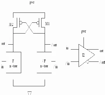
A) ECERL-Efficient Charge Recovery Logic:
Efficient Charge – Recovery Logic (ECRL) proposed by Moon and Jeong [13], shown in Figure 4.1, uses cross-coupled PMOS transistors. It has the structure similar to Cascode Voltage Switch Logic (CVSL) with differential signaling.
It consists of two cross-coupled transistors M1 and
M2 and two NMOS transistors in the
An AC power supply pwr is used for ECRL gates, so as to recover and reuse the supplied energy. Both out
and /out are generated so that the power clock generator can always drive a constant load capacitance independent of the input signal. A more detailed description of ECRL can be found in [13]. Full output swing is obtained because of the cross-coupled PMOS transistors in both precharge and recover phases. But due to the threshold voltage of the PMOS transistors, the circuits suffer from the non-adiabatic loss both in the precharge and recover phases. That is, to say, ECRL always pumps charge on the output with a full swing. However, as the voltage on the supply clock approaches to
Figure 4.1. The Basic Structure of the Adiabatic ECRL Logic.
So the recovery path to the supply clock to the supply clock is disconnected, thus, resulting in incomplete recovery. Vtp is the threshold voltage of PMOS transistor. The amount of loss is given as
EECRL =C|Vtp|2/ 2(4.2)
Thus, from Equation (4.2), it can be inferred that the
non-adiabatic energy loss is dependent on the load capacitance and independent
of the frequency of operation.
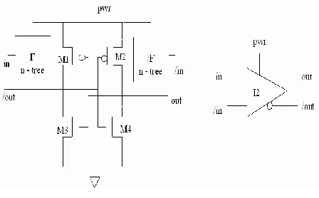
B) Positive Feedback Adiabatic Logic:
The partial energy recovery circuit structure named Positive Feedback Adiabatic Logic (PFAL) [15] has been used, since it shows the lowest energy consumption if compared to other similar families, and a good robustness against technological parameter variations. It is a dual-rail circuit with partial energy recovery. The general schematic of the PFAL gate is shown in Figure 4.3. The core of all the PFAL gates is an adiabatic amplifier, a latch made by the two PMOS M1-M2 and two NMOS M3-M4, that avoids a logic level degradation on the output nodes out and /out. The two n-trees realize the logic functions. This logic family also generates both positive and negative outputs. The functional blocks are in parallel with the PMOSFETs of the adiabatic amplifier and form a transmission gate. The two n-trees realize the logic functions. This logic family also generates both positive and negative outputs.
[image:3.612.80.261.511.674.2]International Journal of Emerging Technology and Advanced Engineering
Website: www.ijetae.com (ISSN 2250-2459, Volume 2, Issue 6, June 2012)327
Figure 4.2
c)Adiabatic Full Adder using PFAL & ECRL
A partially adiabatic logic family PFAL one-bit Full Adder block can be implemented as shown in the Figure 5.23 ( for SUM block) and Figure 5.24 (for OUTPUT_CARRY) below, respectively.
The thesis primarily was focused on the design of low power CMOS cell structures, which is the main contribution of this work. The design of low power CMOS cell structures uses fully complementary CMOS logic style and an adiabatic PFAL logic style. The basic principle behind implementing various design units in the two logic styles is to compare them with reference to the average power dissipated by all of them. A family of full-custom conventional CMOS Logic and an Adiabatic Logic units were designed in Mentor Graphics IC Design Architect using standard TSMC 0.35
µm technology, layout them in Mentor Graphics IC Station and the analysis of the average dynamic power dissipation with respect to the frequency and the load capacitance was done. It was found that the adiabatic PFAL logic style is advantageous in applications where power reduction is of prime importance as in high performance battery-portable digital systems running on batteries such as note-book computers, cellular phones and personal digital assistants.
V.CONCLUSION
With the adiabatic switching approach, the circuit energies are conserved rather than dissipated as heat. Depending on the application and the system requirements, this approach can be used to reduce the
power dissipation of the digital systems. With the help of adiabatic logic, the energy savings of upto 76 % to 90 % [15] can be reached. Circuit simulations show that the adiabatic design units can save energy by a factor of 10 at 50 MHz logically equivalent conventional CMOS implementation and about 2 at 250 MHz, as compared to
VI.FUTURE WORK
(a) ADIAMEMS
To perform digital logic in CMOS in a truly adiabatic (asymptotically thermodynamically reversible) fashion requires that the logic transitions be driven by a quasi-trapezoidal (flat-topped) power-clock voltage waveform, which must be generated by a resonant element with very high Q (quality factor). Recently, MEMS resonators have attained very high frequencies and Q
factors and are becoming widely used in communications system-on-chip (SOC) for RF signal filtering, amplification, etc.
(b)APPLICATION OF NANO-TECHNOLOGY
Carbon nano-tubes grown using Chemical Vapor Deposition (CVD) can be selected to conform to a spiraling shape. Thus, a good quality factor Q can be achieved. The work left to be done for this design would include a method for causing it to keep its form, since nano-tubes are typically not rigid. Also, putting the tube to use in a circuit would lower the effective Q due to the junction discontinuities.
(c) SPACECRAFT
The high cost-per-weight of launching computing-related power supplies, solar panels and cooling systems into orbit imposes a demand for adiabatic power reduction in spacecraft in which these components weigh a significant fraction of total spacecraf
t
weight.References
[1] A. P. CHANDRAKASAN, S. SHENG, AND R. W. BRODERSEN, “Low PowerCMOS Digital Design,” IEEE Journal of Solid-state Circuits, Vol. 27, No. 04, pp. 473-484, April 1999.
[2] H. J. M. VEENDRICK, “Short-circuit Dissipation of Static CMOS Circuitry and itsImpact on the Design of Buffer Circuits,” IEEE JSSC, pp. 468-473, August 1984.
[image:4.612.49.273.136.275.2]International Journal of Emerging Technology and Advanced Engineering
Website: www.ijetae.com (ISSN 2250-2459, Volume 2, Issue 6, June 2012)328
[4] M.HOROWITZ, T.INDENNAUR, AND R. GONZALEZ,“Low Power Digital Design, “Technical Digest IEEE Symposium Low Power Electronics, San Diego, pp. 08-11, October 1994.
[5] T. SAKURAI AND A. R. NEWTON, “Alpha-Power Law MOSET Model and its Applications to CMOS Inverter Delay and other Formulas,” IEEE JSSC, vol. 25, no. 02, pp. 584- 594, October 1990.
[6] A. P. CHANDRAKASAN AND R. W. BRODERSEN, Low-power CMOS digital design, Kluwer Academic, Norwell, Ma, 1995.
[7] SUNG-MO KANG AND YUSUF LEBLEBICI, CMOS Digital Integrated Circuits - Analysis and Design, McGraw-Hill, 2003.
[8] J. S. DENKER, “A Review of Adiabatic Computing,” Technical Digest IEEE Symposium Low Power Electronics, San Diego, pp. 94-97, October 1994.
[9] T. GABARA, “Pulsed Power Supply CMOS,” Technical Digest IEEE SymposiumLow Power Electronics, San Diego, pp. 98- 99, October 1994.
[10] B. VOSS AND M. GLESNER, “A Low Power Sinusoidal Clock,” In Proc. of theInternational Symposium on Circuits and Systems, ISCAS 2001.
[11] W. C. ATHAS, J. G. KOLLER, L. SVENSSON, “An Energy- Efficient CMOS Line Driver using Adiabatic Switching,” Fourth Great Lakes symposium on VLSI, California, March 2005.
[12] T. INDERMAUER AND M. HOROWITZ, “Evaluation of Charge Recovery Circuits and Adiabatic Switching for Low Power Design,” Technical Digest IEEE Symposium Low Power Electronics, San Diego, pp. 102-103, October 2002.
[13] Y. MOON AND D. K. JEONG, “An Efficient Charge Recovery Logic Circuit,” IEEE JSSC, Vol. 31, No. 04, pp. 514-522, April 1996.
[14] A. KAMER, J. S. DENKER, B. FLOWER, et al., “2N2D-order Adiabatic Computation with 2P and 2N-2N2P Logic Circuits,” In Proc. of the International Symposium on Low Power design, Dana Point, pp. 191-196, 1995.
[15] A. BLOTTI AND R. SALETTI, “Ultralow- Power Adiabatic Circuit Semi-Custom Design,” IEEE Transactions on VLSI Systems, vol. 12, no. 11, pp. 1248-1253, November 2004.
[16] S. YOUNIS, T. KNIGHT, “Asymptotically Zero Energy Split-Level Charge Recovery Logic. Proceedings Workshop Low Power Design, Napa Valley, California 1994, pp. 177- 182.
[17] DRAGAN MAKSIMOVIC´, G. VOJIN, OKLOBDŽIJA, BORIVOJE NIKOLIC´ AND K. WAYNE CURRENT, “Clocked CMOS Adiabatic Logic with Integrated Single-Phase Power-Clock Supply,” IEEE Transactions on VLSI Systems, Vol.
08, No. 04, pp. 460-463, August 2000.
[18] A. BLOTTI, S. PASCOLI, AND R. SALETTI, “Sample Model for Positive Feedback Adiabatic Logic Power Consumption Estimation,” Electronics Letters, Vol. 36, No. 2, pp. 116-118, Jan. 2000.