Procedia Engineering 53 ( 2013 ) 225 – 232
1877-7058 © 2013 The Authors. Published by Elsevier Ltd.
Selection and peer-review under responsibility of the Research Management & Innovation Centre, Universiti Malaysia Perlis doi: 10.1016/j.proeng.2013.02.030
Malaysian Technical Universities Conference on Engineering & Technology 2012, MUCET 2012
Part 3 - Civil and Chemical Engineering
Analytical Model and Practicle Validation of Phase Variation of Reflect
array Antenna
M.Inamª
,* and M.Y.Ismailª
ªWireless and Radio Science Centre (WARAS),University Tun Hussein Onn Malaysia, 86400 Batu Pahat , Johor, Malaysia
Abstract
Reflection phase properties of reflect array antenna design in the X-band frequency range has been addressed in this work. An analytical model for obtaining the required reflection phase from individual reflect array elements to form a planar wave in front of the periodic aperture has been presented. A unit cell patch element representing an infinite reflect array modeled based on FEM using the waveguide simulator demonstrated that there is no significant influence on the scattering parameters of reflect array resonant elements until the angle of incidence is increased up to 40 degrees. A Figure of Merit (FoM) has been defined for the comparison of the reflection phase curves of reflect arrays modeled with different dielectric substrates and the results are compared in terms of bandwidth performance and static linear phase range. Furthermore reflect array unit cell patch elements have been fabricated in X-band frequency range using different he practical validation of the waveguide scattering parameter measurements of unit cell reflect array elements. The measured results demonstrated an improvement in FoM and reflect array bandwidth performance with an increase in substrate thickness.
© 2013 The Authors. Published by Elsevier Ltd.
Selection and/or peer-review under responsibility of the Research Management & Innovation Centre, Universiti Malaysia Perlis.
Keywords:reflectarray; progressive phase distribution; scattering parameters; figure of merit
1.Introduction
Reflect array antenna consists of an array of micro strip patches on the grounded dielectric substrate and is illuminated by a primary feed horn which is placed at a particular distance from the array [1]. The individual elements of the array are designed to scatter the incident field with proper phase distribution required to form a planar phase surface in front of the aperture of the reflect array antenna [2]. Due to low cost, compact size and easy deploy ability, reflect arrays are considered as one of the suitable choice for space applications such as deep space exploration and earth remote sensing. However with many advantages of reflect array the major shortcoming occurs when the bandwidth performance is compared with the parabolic reflector [3-5]. Its bandwidth does not exceed much beyond 10% depending on its element design, aperture size and focal length [1]. The constricted bandwidth is largely attributed to the narrow bandwidth of patch elements, the differential spatial phase delay due to extended path length between the feed and the reflect array and the phase errors related to the change in patch size [6]. The feed antenna bandwidth and array element spacing also limits the bandwidth of reflect arrays but these two factors are not serious concerns if the bandwidth requirement is less than 15% [7].
One of the important parameters in the characterization of reflect array antenna design with enhanced bandwidth is the reflection phase performance. This work provides detailed numerical investigations in order to obtain the reflection phase
* Corresponding author. E-mail address: [email protected] © 2013 The Authors. Published by Elsevier Ltd.
curves and compare the performance of reflect array antenna designed with different dielectric materials. The theoretical work has also been validated with the measurements done for the reflect array unit cells designed using different substrate thicknesses. Moreover the measured results are compared with the results obtained by other analysis techniques based on Finite Element Method (FEM) and Finite Integral Method (FIM) used by Ansoft HFSS and CST Microwave Studio respectively.
2.Analytical Modeling
In the absence of a microstrip patch element, the resulting electric field will be the sum of incident and the field reflected from the grounded dielectric slab [4].
tot inc ref
E
E
E
(1)Where, Etotis the total electric field vector, Eincis the incident electric field and
E
ref is the electric field vector for ground plane reflection. But in the presence of the patch element, the resulting field induces a current on the surface of the perfectly conducting patch element and the surface current densityJ
s causes radiation in the presence of grounded dielectric slab to produce scattered electric fields in the dielectric substrate and the air region. Hence the total electric field is given by:tot inc ref scat
E
E
E
E
(2) Where,E
scatis the vector for the electric field scattered by the patch elements. As the surface current Js on the [image:2.544.183.360.375.494.2]conducting patch is varied by applying one of the phasing techniques mentioned above, the scattered electric field varies and produces a change in the reflection phase of a reflect array.
Fig. 1. A unit cell patch element in a waveguide simulator. Top and bottom plane are E-Walls while Left and Right planes are H-Walls
In order to measure the scattering parameters of a linear polarized wave normally incident on the patch element of an infinite reflect array, it has to be assured that minimum mutual coupling between the adjacent elements takes place. The infinite array has been represented by a unit cell patch element using the waveguide simulator technique as shown in Fig. 1. To avoid the grating lobes, the inter-element spacing can be determined by the following conventional array equation.
1 sin
d
(3)Where, d is the distance between two adjacent elements is the operational wavelength and is the angle of the incident wave.
on the reflection loss and resonant frequency of a reflect array designed at 10 GHz using commercially available computer model of Ansoft HFSS.
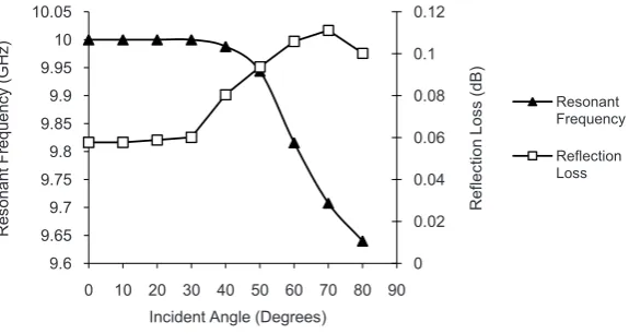
[image:3.544.130.418.126.279.2]It can be observed from Fig. 2 that the reflection loss and resonance frequency of an infinite reflectarray remains almost constant until the incident angle is increased up to 40° showing the appearance of grating lobes and surface waves.
Fig. 2. Effect of incident angle on the reflection loss and resonant frequency
General relation for the calculation of total electric field in the plane of a microstrip radiator for a waveguide simulator technique shown in Fig. 1 can be derived from equation (1) and equation (2) and is given by the following relation [6].
.
1
tot inc
E
G J E
(4)Where, Etot is the vector of tangential electric field,
G
J is the current density,inc
E is the vector of incident electric field and is the reflection coefficient. As the electric field is excited in the Y-direction, the total electric field than can be given by:
,
.
ytot yy y y inc yy
E
G J
E
l G
(5) Where, l is the length of the unit cell patch element and Jy can be given by:y n n
,
n
J
A
x y
(6)Where An Jy
is known, the current on the surface of the patch element can be found out by taking the surface integral of current density as
.
I
J ds
(7)For the calculation of the required reflection phase in order to convert the spherical wave radiated by the feed horn into a planar wave, consider the basic geometry of reflect array shown in Fig. 3. It can be observed from Fig. 3
reflection phase from the individual patch of an array is changing in order to form a planar phase wave in front of aperture. 0
0.02 0.04 0.06 0.08 0.1 0.12
9.6 9.65 9.7 9.75 9.8 9.85 9.9 9.95 10 10.05
0 10 20 30 40 50 60 70 80 90
R
ef
lec
tion
Los
s
(dB)
Res
onant
Frequenc
y
(GHz)
Incident Angle (Degrees)
Resonant Frequency
Fig. 3. Basic geometry of a reflectarray showing the
inter-By using the trigonometric ratio, we can find the required reflected phase from individual patch by:
1
1
tan
;...
0
tan
;...
0
p l
ie
p r
ie
d
k
n
nd
d
k
n
nd
Where, dp is the port distance and die is the distance between two consecutive elements while krand klare angle in
degrees for the patch elements on right and left of the central patch and gives the phase range of the curve and are related with the material properties of substrate used for reflect array design.
3.Analytical Results and Discussions
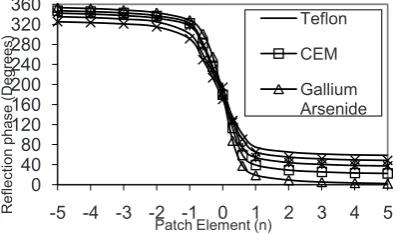
The above equations are used to find out the reflection phase curves for the reflect array designed with different dielectric substrates as shown in Fig. 4. Different materials have been chosen for the reflection phase analysis based on the variety of dielectric permittivity ( r) and loss tangent ( ) values. The reflection phases are characterized using the slopes of the
phase curve and linear static phase range ( s) being depicted in Table I. It can be observed from Table I that the static
[image:4.544.169.368.500.617.2]linear phase range increases with the increase in dielectric permittivity because increasing the permittivity causes the reflection phase curve to get steeper. On the other hand, it can also be observed that materials with lower permittivity values have gentler phase curves. This indicates that Teflon has maximum bandwidth because of lowest slope of the phase curve but the linear static phase.
Fig. 4. Reflection phase curves for different substrate materials
0 40 80 120 160 200 240 280 320 360
-5 -4 -3 -2 -1 0 1 2 3 4 5
R
ef
lec
tion
phas
e
(D
egrees
)
Patch Element (n)
Teflon
CEM
Table 1. Linear Static Phase Range For Different Dielectric Materials
Material Dielectric properties
Linear static phase range ( s)
(°) r
Teflon 2.08 0.0004 165
Rogers 5880 2.20 0.0009 170
CEM 4.50 0.0250 200
Alumina 9.75 0.0003 222
[image:5.544.126.425.64.291.2]Gallium Arsenide 13 0.0004 225
Fig. 5. Geometry of the designed 2 patch element unit cell reflectarray
range of Teflon, as observed from Fig. 4, is much lesser as compared to Gallium Arsenide. Therefore a reflect array designed using lower dielectric permittivity value gives an enhanced bandwidth but at a price of increased phase errors.
4.Measurements Setup
For the scattering parameters measurements, Rogers RT/Duroid with different thicknesses is used to design two identical patch elements reflect array. Two patches are used in order to include the effects of mutual coupling between the patch elements. The geometry of the designed reflect arrays is shown in Fig. 5. The dimensions of the substrate are kept constant
for all designs at L0 x W0
-element, shown in Fig. 5 vary with the dielectric substrate used for reflect array design. A summary of the dimensions for different substrate thickness of Rogers Rt/Duroid 5880 for two patch element reflect array is shown in Table II.
Table 2. Dimensions For Different Substrate Thickness Reflectarrays And Approximate Fabrication Error
Thickness (t)
L1 = L2
Designed Fabricated Fabrication Error
0.127mm 9.5mm 9.1mm 0.4mm
0.381mm 9.38mm 9.2mm 0.18mm
0.508mm 9.3mm 9.2mm 0.1mm
(a) (b) (c)
[image:5.544.160.385.472.537.2]The Reflection loss and reflection phase of the designed samples are measured using Agilent vector network analyzer. An X-band waveguide is designed for the measurement of scattering parameters and is connected to the vector network analyzer using an Agilent coax to waveguide adapter as shown in Fig. 6. The two patch element reflectarray is fixed in the other aperture of the waveguide (Fig. 6 c).
5. Measured Results and Discussion
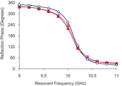
[image:6.544.172.440.239.391.2]The procedure described in Fig. 6 is used to measure the scattering parameter of the fabricated sample and the results are compared with the simulated results obtained by CST MWS and Ansoft HFSS. Fig. 7 shows the simulated and measured reflection phase curves for 0.127mm thick substrate. It can be observed from Fig. 7 that the curves are almost overlapping which shows the validity of the measured results. The slope of the reflection phase curve is very high because the substrate used for the reflect array design is very thin which offers a very high reflection loss and a narrow bandwidth. Fig. 8 shows the simulated and measured reflection phase curves for 0.381mm thick substrate. It can be observed from Fig. 8 that the slope of the measured reflection phase curve is higher as compared to the simulated phase curves.
Fig. 7.Simulated and measured reflection Phase for 0.127mm substrate
Fig. 8. Simulated and measured reflection phase for 0.381mm substrate 0
60 120 180 240 300 360
9 9.5 10 10.5 11
R
ef
elec
tion P
has
e
(De
grees
)
Resonant Frequency (GHz)
CST MWS
Ansoft HFSS
Measured
0 60 120 180 240 300 360
9 9.5 10 10.5 11
R
ef
lec
tion
Phas
e
(De
grees
)
Resonant Frequency (GHz)
CST MWS
Ansoft HFSS
[image:6.544.168.382.437.587.2]Fig. 9. Simulated and measured reflection phase for 0.508mm substrate
[image:7.544.178.438.64.215.2]The reason for this difference is the discrepancy in the measured and simulated reflection losses which is caused by the material properties and losses due to connectors during measurements.
Fig. 9 shows the comparison of measured and simulated reflection phase plots of the rectangular reflectarray elements constructed on 0.508mm thick substrate. A close agreement can be observed between the two curves. Furthermore it can be observed that the simulated and measured reflection phase curves of 0.508mm thick substrate show lesser slope as compared to the curves of 0.127mm and 0.381mm thick substrates.
In order to compare the reflection phase performance of reflect array unit cells designed with different thickness, a figure of merit (FoM) as defined in [7] has been used. FoM is the ratio of the change in reflection phase to the change in the frequency and it can be expressed as.
FOM f
°/ MHz (8)
Where is the change in the reflection phase in degrees and is the change in the resonant frequency in MHz of the reflect array antenna and FoM is calculated here in °/MHz. Table III provides a summary of results for linear static phase and FoM measured for unit cells fabricated on different substrate thickness of Rogers 5880 substrate.
Table 3. Fom For Unit Cells Constructed On Different Substrate Thicknesses
Substrate thickness
(mm)
Linear static phase range ( s)
(°)
FoM
(°/MHz )
0.127 240 0.32
0.381 190 0.30
0.508 180 0.29
As depicted in Table III, the unit cells designed with 0.127mm thick substrate is shown to offer a higher FoM of 0.32°/MHz as compared to FoM of 0.29°/MHz shown by 0.508 mm thick reflectarray unit cell. These results can be related to the fact that increasing the substrate thickness has the same effect as decreasing the dielectric permittivity of the material. Therefore thicker substrates provide lower FoM and hence phase errors reduce. However it can also be observed from Table III that the thicker substrate (0.508mm) provides a lower value of linear static phase range which depicts degradation in bandwidth of reflect array antenna.
6.Conclusion
A technique for the measurement of the required reflection phase from the individual element of a reflect array to form a planar wave in front of aperture is presented. The independence of the scattering parameters from the angle of incident below a certain value for an infinite reflect array, designed using waveguide simulator technique has been demonstrated based on FEM analysis. The technique for the scattering parameter measurements of infinite reflect arrays has been
0 60 120 180 240 300 360
9 9.5 10 10.5 11
R
ef
lec
tion
Phas
e
(D
egrees
)
Resonant Frequency (GHz)
CST MWS
Ansoft HFSS
[image:7.544.171.376.425.499.2]presented using different commercially available dielectric materials. The measured results are compared with the simulated results and a close agreement has been demonstrated. Moreover the trade-off between the bandwidth performance and phase errors of single frequency reflect array design has been demonstrated for both simulated and measured results.
Acknowledgement
The authors would like to thank the staff of Wireless and Radio Science Centre (WARAS) of University Tun Hussien Onn Malaysia (UTHM) for the technical support.
References
[1] J. ectarray Antenna for Microspacecraft Applications, Spacecraft Telecommunications Equipment section, TDA Progress report 42-12, February 15,1995.
[2] D. M. Pozar, S. D. Targoski and H. r Wave Microstrip Reflectarrays, IEEE Transactions on Antennas propagation, Vol.45, No. 2, pp. 287-296, 1997.
[3] J. Huang and J. Encinar, Reflectarray Antennas, Wiley, Interscience, 2007.
[4] T. A. Metzeler, Design and Analysis of a Microstrip Reflectarray, University of Massachusetts, February 1993.
[5] M. E. Bialkowski and F. by Microstrip Patches and Slots, Microwave and Optical
Technology Letters, Vol. 36, No3, pp. 206-210, 2003.
[6] M. S. Gashinova and O. G. Reflectarray Antenna, Progress in Electromagnetic Research Symposium, Cambridge, USA, pp. 133-136, March 2006.
[7] M. Y. Ismail and M. as Based on Material