http://dx.doi.org/10.4236/jmp.2014.518203
Deep Level Transient Spectroscopy of
AlGaInP LEDs
M. Atiq1,2, Nazir A. Naz1, Akbar Ali1,2
1Department of Applied Physics, Federal Urdu University of Arts, Science and Technology, Islamabad, Pakistan 2Department of Basic Sciences, Riphah International University, Islamabad, Pakistan
Email: [email protected], [email protected]
Received 8 October 2014; revised 5 November 2014; accepted 1 December 2014
Copyright © 2014 by authors and Scientific Research Publishing Inc.
This work is licensed under the Creative Commons Attribution International License (CC BY). http://creativecommons.org/licenses/by/4.0/
Abstract
Deep level transient spectroscopy (temperature scans) of AlGaInP based red light emitting diodes was carried out from 77 K to room temperature. At least ten defects were observed. Of these, five defects assigned to energy states 0.21, 0.22, 0.24, 0.26, and 0.24 eV were characterized. Respective capture cross-sections, measured at infinite temperature (T = ∞), were found to be 8.84 × 10⁻¹⁶, 6.98 × 10⁻¹⁶, 7.86 × 10⁻¹⁶, 9.9 × 10⁻¹⁶ and 2.1 × 10⁻¹⁶ cm2. Corresponding concentrations of defects were 3.7 × 10¹³, 3.5 × 10¹³, 3.2 × 10¹³, 3.3 × 10¹³ and 3.1 × 1013 cm−3.
Keywords
Semiconductors, MOCVD, Defects, DLTS
1. Introduction
Recently a variety of light emitting diodes (LEDs), based on compound semiconductors have attracted consi-derable attention due to their structural versatility and unique properties [1] [2] such as high brightness and di-rectionality, improved daytime visibility of various commercial outdoor displays, automobile indicators, traffic signals and use in high density external storage system [2]-[9]. AlGaInP based diodes, which emit wavelengths ranging from red to yellow green, are playing important role in the industry [1] [10] [11]. Although a high in-ternal quantum efficiency has been achieved for AlGaInP based LEDs, however, exin-ternal efficiency yet shows deterioration due to strong light absorption in GaAs substrate [1] [8] [9]. The main challenging issue is to im-prove the efficiency and the power loss of AlGaInP based LEDs.
in-sufficient for considering microscopic factors such as deep level defects that influence emission properties and laser performance [10] [12] [13]. Deep levels due to defects in AlGaInP materials act as non-radiative recombi-nation and trapping centers, and significantly decrease the radiative efficiency and increase the thresh hold cur-rent density [10]. Study of defects in AlGaInP is, therefore, of great importance to improve the performance of the devices. In this article, we present a study of defects in AlGaInP, using Deep Level Transient Spectroscopy (DLTS).
2. Samples
Single color, high bright, low power consumption, highly reliable and long life light emitting diodes (LEDs) manufactured by Hebei IT, China [14] were imported. The diodes emit super bright red color (wavelength ~632 nm) under 2 volts (forward bias) and 20 mA current at 25˚C. The maximum reverse current at 25˚C is 30 µA under reverse voltage of 5 volts, suitable for DLTS measurements.
3. Measurements
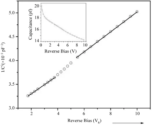
Capacitance-voltage (C-V) characteristics, shown in the inset of Figure 1, were measured at room temperature using capacitance meter, Boonton model 7200, [15]. 1/C2 verses reverse bias plot is shown in Figure 1. Data was found to fit on two straight lines indicating almost uniform concentrations of acceptors and donors (Na
and Nd) in n and p sides of the PIN junction [16]. The concentrations were found to nearly same on both
p and n sides of the junction.
[image:2.595.183.446.490.707.2]After C-V measurements, DLTS [17] of the samples has been carried out with a very sensitive machine DLS- 83D, manufactured by Semitrap, Hungry [18]. This machine monitors emission of electrons or holes in deple-tion region of a juncdeple-tion. Temperature of the samples was decreased to 77 K by lowering the sample holder into liquid nitrogen container and increased with the help of a heater embedded in the holder during temperature scans. DLTS scans with different repetition rates were recorded using reverse voltage VR=3 V and filling pulse tp =500 μsec. Two typical temperature scans recorded with repetition rates of 5 Hz and 80 Hz are shown as spectrum (a) and (b) inFigure 2, respectively. In the case of PIN diodes, DLTS signal from both n- and p- sides of the junction is possible, therefore, peaks, due to signals, can appear from either side of the junction. DLTS scans depict at least ten peaks named as P1, P2, P3, P4, P5, P6, P7, P8, P9, and P10, shown as spectrum (a) and (b) inFigure 2. Peak temperatures were noted for each scan and log
(
e T2)
verses 1000/T was plotted corresponding to each peak on semi-log scale as shown inFigure 3. From the slopes and intercepts at T = ∞ of the best fit lines through the data points, activation energies and capture cross-sections, respectively, were calculated using the equation [17],Figure 2. DLTS, temperature scans recorded at (a) 5 Hz
[image:3.595.208.418.85.349.2]and (b) 80 Hz of AlGaInP LEDs.
Figure 3.T2 corrected Arrhenius plots of AlGaInP LEDs.
(
)
, , ,exp
n p n pn th c v A B
e =gσ v N − E − ∆T S k T (1)
where, en p, is the electron/hole emission rate at temperature T, g is the degeneracy factor which, for
sim-plicity, is taken as one, ∆S is the entropy change, EA is the thermal activation energy
(
ET −EV)
of thede-fect state, σn p, the electron /hole capture cross section, vth , the average thermal velocity of the electron/hole,
,
c v
N the effective density of states in the conduction/valence band and kB the Boltzmann’s constant.
4. Results and Discussion
[image:3.595.209.417.382.556.2]Table 1. Characteristics of defects assigned to different peaks. EA, σ∞ and NT, represent thermal activation energy, apparent
capture cross-section and concentration of deep levels, respectively.
Peaks P3 P4 P5 P6 P7
A
E (eV) 0.21 0.22 0.24 0.26 0.24
( )σ∞ (×10−19 cm−2) 1.1 0.87 0.98 1.2 0.26
T
N (×1013 cm−3) 3.7 3.5 3.2 3.3 3.1
repetition rates of 5 Hz and 80 Hz, shown inFigure 2(a) andFigure 2(b), respectively, are presented to show all peaks.
Only two data points could be recorded for peaks P1, P2, P8 and P9. Peak P10 appeared only in one scan taken with 80 Hz because our experimental setup did not allow to measure beyond room temperature. The ap-pearances of the peaks P1 and P2 in higher frequency and P8 and P10 in lower frequency DLTS scans are quite natural. Calculations for thermal activation energies, capture cross-sections and concentrations of defects as-signed to P1, P2, P8 and P10 are not reliable, therefore, not mentioned here. The activation energies obtained for the defects, P3-P7 are 0.21, 0.22, 0.24, 0.26 and 0.24 eV, and corresponding capture cross-sections calculated from the intercepts are 1.1 × 10⁻¹⁹, 8.7 × 10⁻²⁰, 9.8 × 10⁻²⁰, 1.2 × 10⁻¹⁹ and 2.6 × 10⁻²⁰ cm2, respectively. The respective concentrations of the defects are 3.7 × 10¹³, 3.5 × 10¹³, 3.2 × 10¹³, 3.3 × 10¹³ and 3.1 × 1013 cm−3, re-spectively. The above data are also listed inTable 1.
Sugiura et al. [19] have reported three defects D1, D2 and D3 in MOVPE grown AlGaInP layer, correspond-ing to energies, 0.43, 0.5 and 1.3 eV, respectively. Among these, D3 was attributed to Aluminum related defect, while D1 and D2 were not identified. On comparison, it is found that our emission rate data do not show any matching to those reported by Sugiura et al. Byungjin et al. [8] detected a defect related peak corresponding to energy 0.2 eV in their DLTS spectra of AlGaInP taken under two different ambient i.e. H2 and N2. While, Kim et al. [10] observed two DLTS peaks corresponding to energy states, 0.35 - 0.36 and 0.48 - 0.5 eV in their four multiple quantum well (MQW) structured AlGaInP samples grown by MOCVD. None of the emission rate data of our defects were found to similar with the above published data. Defects reported in our work are, therefore, different to those reported by other researchers. Most probably the defects are induced during growth either due to lattice mismatch or lattice imperfections or complexes formed due to high reactivity at atomic scale. These defects may act as radiative or non-radiative defects. If the defects act as a non-radiative recombination center
[20], they will degrade the emission efficiency of the material. We doubt that among these defects few may act as such centers. For better emission output, such defects should be tightly controlled. As the material is relative-ly new, and the knowledge about the defects in this material is severerelative-ly lacking in literature, DLTS study of the material is, therefore, of vital importance. Detailed work is in progress for obtaining a comprehensive picture of defects in the material.
Acknowledgements
DLTS measurements have been performed in Semiconductor Physics Laboratory, Quaid-i-Azam University, Is-lamabad, Pakistan.
References
[1] Kuo, D.-M., Wang, S.-J., Uang, K.-M., Chen, T.-M., Lee, W.-C. and Wang, P.-R. (2011) Applied Physics Express, 4, Article ID: 012101. http://dx.doi.org/10.1143/APEX.4.012101
[2] Lee, Y.-J., Lee, C.-J. and Chen, C.-H. (2011) Japanese Journal of Applied Physics, 50, Article ID: 04DG18. [3] Gessmann, Th. and Schubert, E.F. (2004) Journal of Applied Physics, 95, 2203. http://dx.doi.org/10.1063/1.1643786
[4] Lin, R.M., Li, J.C., Chou, Y.L. and Wu, M.C. (2006) IEEE Photonics Technology Letters, 18, 1642-1644.
http://dx.doi.org/10.1109/LPT.2006.879524
[5] Krames, M.R., Shchekin, O.B., Regina, M.M., Mueller, G.O., Zhou, L., Harbers, G. and Craford, M.G. (2007) Journal of Display Technology, 3, 160-175. http://dx.doi.org/10.1109/JDT.2007.895339
[6] Lee, Y.J., Lu, T.C., Kuo, H.C. and Wang, S.C. (2007) Journal of Display Technology, 3, 118-125.
[7] Lee, Y.J., Lin, P.C., Lu, T.C., Kuo, H.C. and Wang, S.C. (2007) Applied Physics Letters, 90, Article ID: 161115. [8] Ma, B., Cho, S., Lee, C., Lee, S., Kang, J., Kim, B., Kang, D., Shin, Y., Kim, Y., Kim, T. and Park, Y. (1974)
Japa-nese Journal of Applied Physics, 45, 774-777. http://dx.doi.org/10.1143/JJAP.45.774
[9] Yagi, T., Nishiguchi, H., Yoshida, Y., Miyashita, M., Sasaki, M., Sakamoto, Y., Ono, K.-I. and Mitsui, Y. (2003) IEEE Journal of Selected Topics in Quantum Electronics, 9, 1260. http://dx.doi.org/10.1109/JSTQE.2003.819514
[10] Kim, D.S., Kim, K.C., Shin, Y.C., Kang, D.H., Kim, B.J., Kimb, Y.M., Park, Y., Kim, T.G., Kim, D.S., et al. (2006)
Physica B, 376-377, 610-613. http://dx.doi.org/10.1016/j.physb.2005.12.154
[11] Shima, A., Tada, H., Ono, K., Fujiwara, M., Utakouji, T., Kimura, T., Takemi, M. and Higuchi, H. (1997) IEEE Pho-tonics Technology Letters, 9, 413-415. http://dx.doi.org/10.1109/68.559372
[12] Domen, K., Sugiura, K., Anayama, C., Kondo, M., Sugawara, M., Tanahashi, T. and Nakajima, K. (1991) Journal of Crystal Growth, 115, 529-532. http://dx.doi.org/10.1016/0022-0248(91)90799-B
[13] Kaniewska, M., Kryńska, D. and Wesołowski, M. (2001) Optical Materials, 17, 283-286.
http://dx.doi.org/10.1016/S0925-3467(01)00093-3
[14] Data Sheet. Hebei International Trading (Shanghai) Co., Ltd.
[15] Instruction Manual, Capacitance-Meter, Boonton 7200. Boonton Electronics Corporation, Boonton.
[16] Tsarova, T., Wosinski, T., Kosa, A.M., Skierbiszewski, C., Grzegory, I. and Perlin, P. (2007) Acta Physica Polonica A,
112, 331-337.
[17] Lang, D.V. (1974) Journal of Applied Physics, 45, 3023. http://dx.doi.org/10.1063/1.1663719
[18] Operating Manual, Deep Level Transient Spectrometer, Serni Lab “DLS-83D”, Meunipex, Budapest, 1981.
[19] Sugiura, K., Domen, K., Sugawara, M., Anayama, C., Kondo, M., Tanahashi, T. and Nakajima, K. (1991) Journal of Applied Physics, 70, 4946-4949.