LEABHARLANN CHOLAISTE NA TRIONOIDE, BAILE ATHA CLIATH TRINITY COLLEGE LIBRARY DUBLIN OUscoil Atha Cliath The University of Dublin
Terms and Conditions of Use of Digitised Theses from Trinity College Library Dublin
Copyright statement
All material supplied by Trinity College Library is protected by copyright (under the Copyright and Related Rights Act, 2000 as amended) and other relevant Intellectual Property Rights. By accessing and using a Digitised Thesis from Trinity College Library you acknowledge that all Intellectual Property Rights in any Works supplied are the sole and exclusive property of the copyright and/or other I PR holder. Specific copyright holders may not be explicitly identified. Use of materials from other sources within a thesis should not be construed as a claim over them.
A non-exclusive, non-transferable licence is hereby granted to those using or reproducing, in whole or in part, the material for valid purposes, providing the copyright owners are acknowledged using the normal conventions. Where specific permission to use material is required, this is identified and such permission must be sought from the copyright holder or agency cited.
Liability statement
By using a Digitised Thesis, I accept that Trinity College Dublin bears no legal responsibility for the accuracy, legality or comprehensiveness of materials contained within the thesis, and that Trinity College Dublin accepts no liability for indirect, consequential, or incidental, damages or losses arising from use of the thesis for whatever reason. Information located in a thesis may be subject to specific use constraints, details of which may not be explicitly described. It is the responsibility of potential and actual users to be aware of such constraints and to abide by them. By making use of material from a digitised thesis, you accept these copyright and disclaimer provisions. Where it is brought to the attention of Trinity College Library that there may be a breach of copyright or other restraint, it is the policy to withdraw or take down access to a thesis while the issue is being resolved.
Access Agreement
By using a Digitised Thesis from Trinity College Library you are bound by the following Terms & Conditions. Please read them carefully.
Spin Valves and their Application
by
Emma Kerr
A thesis submitted fo r the degree o f Doctor o f Philosophy in the
University o f Dublin
Department of Physics
Trinity College Dublin
Declaration
This thesis is subm itted by the undersigned for exam ination for the degree o f Doctor o f Philosophy at the University o f Dublin. It has not been subm itted as an exercise for a
degree at any other university.
This thesis, apart from the advice, assistance and jo in t effort m entioned in the acknow ledgm ents and in the text, is entirely my own work.
I agree that the library may lend or copy this thesis freely on request.
Summary
The discovery o f giant m agnetoresi stance (GM R) in the late 1980’s resulted in massive interest in the deposition and characterisation o f artificial layered m agnetic structures. Spin valves were discovered in 1991 and have been the subject o f intense interest due to their suitability for application in m agnetoresistive read heads in m agnetic hard disk drives. The basic elem ent o f a spin valve is tw o ferrom agnetic layers separated by a non-m agnetic spacer. The electrical resistance o f the structure is low when the m agnetisation directions o f the ferrom agnetic layers are aligned parallel and high when they are antiparallel. One of the ferrom agnetic layers, the free layer, switches m agnetisation direction close to zero field. The other layer, the pinned layer, is grown next to an antiferrom agnet and its m agnetisation direction is pinned at low fields. Switching o f the free layer at low fields, therefore, results in a transition from the parallel to antiparallel state and a linear change in resistance. Hence the spin valve is a highly sensitive m agnetic field sensor and can be used in several applications. Spin valves can also be considered as one o f the fundamental building blocks necessary for developing more com plicated spin electronic devices.
In this work, several aspects o f spin valves have been investigated. Chapter 1 is an introduction to spin valves and describes the fundam ental physical principles involved as well as the m ain applications. C hapter 2 describes the experim ental techniques used in this w ork to deposit, characterise and pattern spin valves.
In general, spin valves require a post-deposition m agnetic anneal to establish exchange
bias. Chapter 4 presents a study o f the effect o f the strength o f the m agnetic annealing
field on param eters such as exchange bias and G M R in spin valve structures. A
specifically designed furnace allow ed m agnetic annealing o f spin valves to be perform ed in
a superconducting m agnet at fields up to 5.5 T. A m agnetic field effect was found in
bottom pinned structures and is discussed in term s o f a re-alignm ent o f the IrM n pinned
spin moment.
Interest in patterning m agnetic nanostructures using the Focussed Ion Beam (FIB) has
increased in recent years. However, im plantation o f Ga^ ions from the beam can have
adverse effects on the m agnetic and electrical properties o f m agnetic thin films and
m ultilayers. In chapter 5, the effects o f Ga+ ion im plantation in IrMn spin valves is
presented and the feasibility o f using FIB m illing as a tool for nano-pattering spin valves
assessed.
Finally, an interesting application o f a spin valve is presented in Chapter 6. The m ixed
sensor consists o f a superconducting loop with a m icron-sized constriction. A spin valve
sensor is deposited above or below the constriction. In perpendicular applied fields,
supercurrents in the loop create a locally enhanced in-plane m agnetic field above the
constriction. This field can be detected by the spin valve. The optim isation o f the spin
valve structure for this specific application is discussed and results for a m ixed sensor
prototype presented. The sensitivity o f the prototype is com parable to that o f high Tc
Acknowledgements
I would like to thank Prof. Coey for giving me the opportunity to work in his group and for his supervision and guidance during the last four years. Even w ith his hectic schedule, he alw ays m akes time to see his students. I was also lucky enough to have Sebastiaan van Dijken on hand who provided guidance on a daily basis. His expertise, both in the lab and with writing up was a huge help. During my work I was involved in collaboration with Claude Ferm on and M yriam Pannetier in Paris. It was a great experience for me to be involved w ith this w ork and to visit another lab. Thanks for the hospitality and for the help with the write-up. Thanks also to Frederic Ott for his help w ith the neutron work.
Table o f Contents
C h a p te r!
I n tr o d u c tio n ...10
1.1 Spin Electronics... 10
1.2 Giant Magnetoresistance... 11
1.3 Spin valve structures...17
1.3.1 Interlayer coupling in spin valves...20
1.4 Exchange b ia s ... 22
1.4.1 Exchange bias materials and properties...28
1.5 Spin valve designs...31
1.6 Spin valves devices...34
1.6.1 Spin valves as magnetic-field sensors... 36
1.6.2 Spin valves in read heads... 37
1.6.3 Spin valves in M RAM ...40
1.7 References...41
C h a p te r 2 E x p e rim e n ta l T e c h n iq u e s ...45
2.1 Magnetron sputtering in the Shamrock Deposition Tool... 45
2.1.1 M agnetron Sputtering...45
2.1.2 The Shamrock...46
2.2 Magnetoresistance measurements...51
2.3 Noise Measurements...51
2.4 Superconducting Quantum Interference Device (SQU ID )... 52
2.5 Magnetic annealing...52
2.6 X-ray Diffraction... 54
2.7 Polarised Neutron Reflectometry... 56
2.7.1 Principles o f neutron reflectivity... 56
2.7.2 Neutron-matter interaction... 57
2.7.3 Reflectivity on Non-Magnetic Systems...58
2.7.4 Neutron reflectivity on magnetic system s...60
2.7.5 Interaction of the neutron with a magnetic layer... 61
2.8 Fabrication of small magnetic structures... 65
2.8.1 Optical Lithography...65
2.8.2 Focused Ion Beam (FIB) to o l... 69
2.9 References...72
C h a p te r 3 C h a ra c te ris a tio n o f S p in V a lv e s u sin g P o la riz e d N e u tro n R e fle c to m e try 73 3.1 Introduction...73
3.2 Structural and magnetic characterisation of spin valves... 74
3.2.1 Deposition and Magnetotransport... 74
3.2.2 Structural characterisation using X-Ray Reflectom etry...75
3.2.3 Structural and magnetic characterisation using P N R ... 77
3.2.4 Measurement of the spin valve thermal stability... 81
3.3 Conclusion...86
3.4 References...87
C h a p te r 4 In flu e n c e o f th e A n n e a lin g F ie ld S tre n g th on E x c h a n g e B ia s an d M a g n e to re sista n c e o f S p in V a lv e s w ith I r M n ... 88
4.1 Introduction...88
4.2 As-deposited spin v alv es...91
4.3 Influence of the annealing tem perature...95
4.4 Influence o f the annealing field... 101
4.5 Conclusion... 108
4.6 References... 109
C h a p te r 5 E ffe c ts o f Ga^ ion im p la n ta tio n o n th e m a g n e to re s is tiv e p ro p e rtie s o f spin v a lv e s w ith I r M n ... 111
5.1 Introduction... I l l 5.2 Direct implantation o f Ga^ ions... 113
5.4 C o n clu sio n ... 123
5.5 R eferences... 124
Chapter 6 Fem totesla M agnetic field M easurement with a Spin V alve S en so r 125 6.1 Introduction... 125
6.2 Design o f the spin valve elem ent o f the m ixed s e n s o r...128
6.2.1 N oise in spin v a lv e s... 128
6.2.2 Spin valve desig n ... 129
6.2.3 Spin valve sensitivity... 132
6.3 The principle o f the m ixed sensor d ev ic e... 133
6.4 Sample prep aratio n ... 136
6.5 Fem totesla resolution with an YBCO-spin valve m ixed se n so r...138
6.6 Fem totesla resolution with a Nb-spin valve m ixed se n so r...141
6.7 C onclusion...143
6.8 References... 145
Chapter 7 C onclusions and Future W ork...147
Publications... 151
Table o f Figures
Chapter 1
Figure 1.1 The original GM R observation o f G M R in (Fe/Cr)n m ultilayers by Baiblich et al [3] reporting G M R effects o f up to 45% requiring saturating fields o f up to 2 T ...11 Figure 1.2 Density o f states o f transition m etals Fe, Co, N i and Cu from [ ] ... 13 Figure 1.3 Resistor m odel o f G M R ... 14 Figure 1.4 Current in plane (left) and current perpendicular to plane (right) GM R
geom etries...16 Figure 1.5 Schematic o f m agnetisation (left) and m agnetoresistance (right) o f a pseudo
spin v a lv e ... 18 Figure 1.6 M agnetoresistance (top) and m agnetisation (bottom ) o f an exchange biased
spin valve...19 Figure 1.7 Free layer reversal o f a spin valve... 20 Figure 1.8 Schematic showing ferromagnetic m agnetostatic Neel coupling between
two ferromagnetic layers separated by a non-m agnetic spacer... 21 Figure 1.9 Hysteresis o f Co/CoO particles m easured at 77 K after cooling under a m agnetic field o f 1 T (1) and zero field (2) [22]...23 Figure 1.10 Phenom enological description o f exchange b ia s ...24 Figure 1.11 M agnetotransport curve o f SAF spin valve w ith stack com position shown....
... 33 Figure 1.12 Spin valve deposited with crossed anisotropy (a) and parallel anisotropy (b)
...35 Figure 1.13 Schematic cross section o f a vertical read -head above a storage recording
Chapter 2
Figure 2.1 Cross section schematic o f the S-Gun m ag n etro n ... 46
Figure 2.2 The sham rock sputtering tool in the CIN SE class 1000 c lean ro o m ... 47
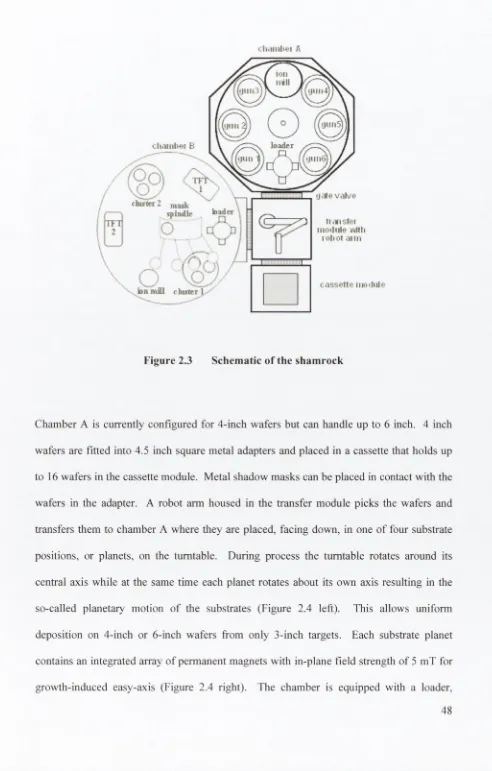
Figure 2.3 Schem atic o f the sham rock... 48
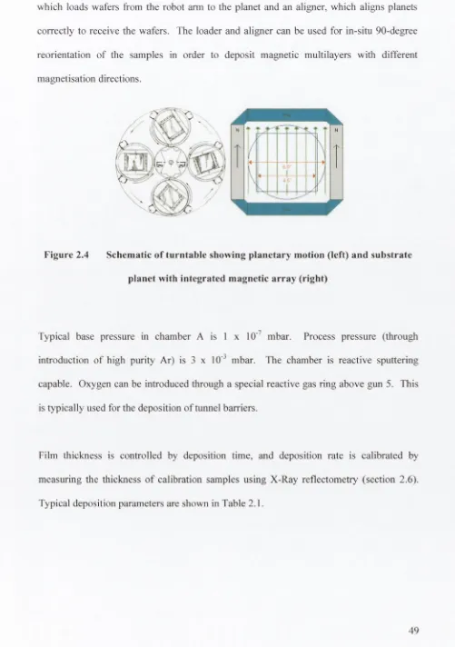
Figure 2.4 Schematic o f turntable showing planetary m otion (left) and substrate planet w ith integrated m agnetic array (rig h t)...49
Figure 2.5 Four point m agnetoresistance m easurem ent...51
Figure 2.6 Cross-section schem atic o f m agnetic fiamace inside superconducting 5.5 T C ryogenics m a g n e t... 53
Figure 2.7 Schematic o f XRR s e t-u p ...55
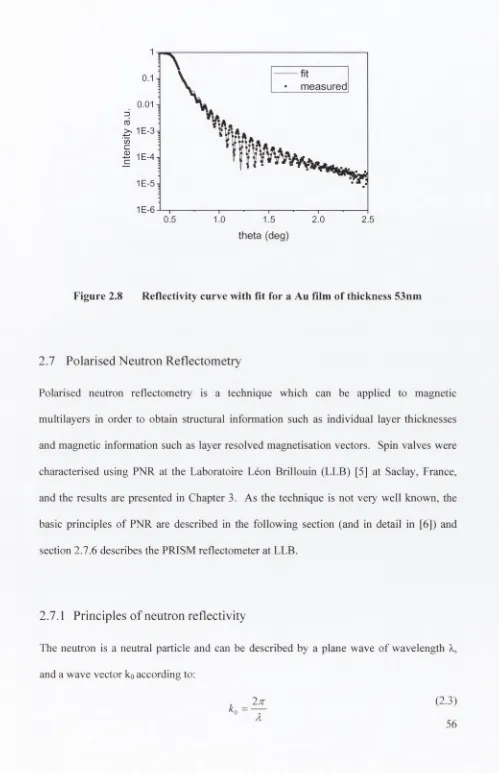
Figure 2.8 Reflectivity curve with fit for a Au film o f thickness 53nm ... 56
Figure 2.9 Schem atic o f axis notation used for reflection from a s u rfa c e ...58
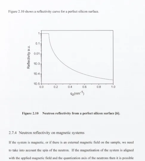
Figure 2.10 N eutron reflectivity from a perfect silicon surface [6]... 60
Figure 2.11 Up and down reflectivities on a nickel thin film [6]... 62
Figure 2.12 Schematic o f the experimental set-up; (a) top view, (b) side view. The different elements are: m ultilayer m onochrom ator (M), deviator guide (D), focusing guide (C), collim ation slits (S1-S4), flippers (FI and F2), transmission polarizer (P) and reflection analyzer (A). Fabrication o f small m agnetic structures...64
Figure 2.13 Six steps involved in the standard patterning p ro ce d u re ... 67
Figure 2.14 5 steps for lift-off p rocedure... 68
Figure 2.15 The dual beam FIB tool in the Class 1000 cleanroom ...70
Chapter 3
Figure 3.1 Free layer reversal o f crossed anisotropy spin valve structure T a(5nm )/N iFe(3.5nm )/C oFe(I.2nm )/C u(2.9nm )/C oFe(2.5nm )/IrM n(10nm )/ T a (lO n m )...50 Figure 3.2 X R R curve with fit o f spin valve stru ctu re ... 51 Figure 3.3 Schematic showing spin valve m easurem ent configuration for and R“
intensities for free and pinned layer parallel (left) and free and pinned layer antiparallel (right)...52 Figure 3.4 Reflectivity curves for spin valve with tNiPe = 2nm in the parallel (a) and
anti-parallel (b) configuration. Red squares R^^, blue squares R" best fit in red and blue lines. Table showing spin valve structure as determ ined by fits to the reflectivity curves...52 Figure 3.5 Reflectivity curves for spin valve with tNiPe = 2nm in the parallel (a) and
anti-parallel (b) configuration. Red squares R^^, blue squares R' best fit in red and blue lines. Table showing spin valve structure as determ ined by fits to the reflectivity curves...53 Figure 3.6 Reflectivity curves for spin valve with tNiPe = 5nm in the parallel (a) and
Chapter 4
Figure 4.1 Figure 4.2 Figure 4.3 Figure 4.4 Figure 4.5 Figure 4.6 Figure 4.7 Figure 4.8 Figure 4.9 Figure 4.10Chapter 5
Figure 5.1 M agnetoresistance and m agnetisation curves for the as-deposited spin valve structure... 114 Figure 5.2
Figure 5.3
Figure 5.4 Figure 5.5
Figure 5.6 Figure 5.7 Figure 5.8
Figure 5.9
Chapter 6
Figure 6.1
Figure 6.2 Figure 6.3
Figure 6.4
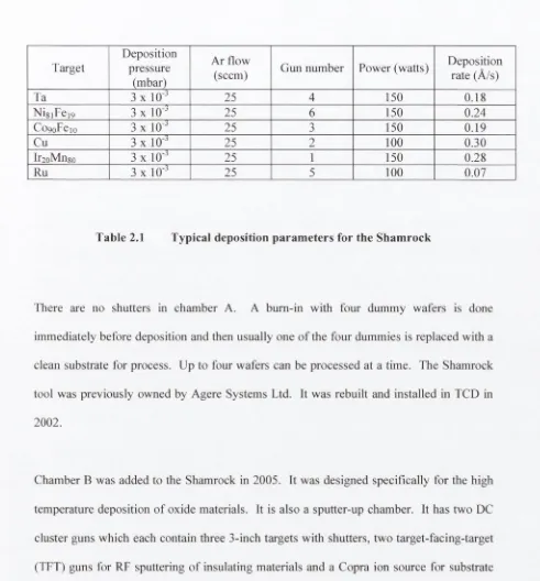
M agnetoresistance o f im planted spin v a lv e s ...115 spin valve resistance (filled sym bols) and m agnetoresistance (open symbols) as a function o f ion dose (lines are guides to the eye)... 116 N orm alised exchange bias field as a fiinction o f ion d o se ... 117 TRIM sim ulation showing 30 keV Ga^ ion distribution throughout the spin valve structure... 117 N orm alised MR and AR as a function o f ion dose (line is a guide) 119
SEM o f spin valve lines FIB m illed to different w idths...120 M agnetoresistance o f FIB m illed spin valves with line widths ranging from 10 [am to 0.5 |.im ...121
(a) Resistance (b) AR and (c) m agnetoresistance as a function o f 1/linewidth for FIB m illed spin v a lv e s ...122
Figure 6.5 Schem atic o f the superconducting loop when an external perpendicular field is applied. The supercurrent (w hite arrows) generates a high density o f field lines with an in-plane com ponent at the position o f the constriction. The spin valve sensor is placed im m ediately above or b elow the constriction. 133 Figure 6.6 Schem atic view s o f Y BCO m ixed sensor device. (A ) Schem atic show ing
Y BCO superconducting loop with yoke-shaped spin valve sensor and four contacts for measurement. (B ) Optical micrograph o f the constricted area o f the loop under the active part o f the spin valve. (C) Cross-section o f the spin valve stack show ing the in-plane com ponents o f the field created by the Y BCO flux-to field transformer. (D ) C ross-section o f the d evice show ing electrical isolation o f the spin valve and the contacts from the loop by the SisN4 layer... 135 Figure 6.7 Schem atic o f patterning process for the Y B C O -based m ixed sensor d e v ic e ..
...137 Figure 6.8 M agnetoresistance o f the spin valve yok e o f an YBC O -based m ixed sensor
at 4.2 K...138 Figure 6.9 M agnetoresistance ratio as a function o f temperature... 139 Figure 6.10 M agnetoresistance as a ftinction o f perpendicular applied field at 4 .2 K on
the Y BC O device. The inset show s the gain as a function o f temperature. ...140 Figure 6.11 N o ise spectra o f the Y BC O m ixed sensor at 4.2K and 77K with 15 m A and 5 mA o f sensing current respectively... 141 Figure 6.12 M agnetoresistance as a function o f perpendicular applied field at 4.2 K for the Nb based m ixed sensor... 142 Figure 6.13 N o ise spectra o f the Nb device at 5 K with 0 m A and 1 mA sensing current.
... 143
Chapter 1
Introduction
1.1 S pi n E l e c t r o n i c s
O ver the last ten years, Spin Electronics has becom e an exciting area o f research and developm ent com bining the two traditional areas o f m agnetism and electronics. Conventional electronics is based on m anipulating and controlling a current flow by applying an electric field, which acts as a force on the charge o f electrons. Another interesting property o f the electron is its spin. This is an intrinsic property resulting from the fact that the electron behaves as if it were spinning on its own axis thereby creating a m agnetic m om ent. This spin angular m om entum is quantized and can take only two
values: + /z/2 (spin up) and - ^ / 2 (spin down), w here /j is Plank’s constant. N on-m agnetic
1.2 Giant Magnetoresistance
In the last thirty years, huge technological advances have been m ade in the fields o f thin films deposition and m aterials preparation. This has allow ed developm ent o f a w ealth o f artificially constructed m ultilayer systems com bing m agnetic, non-m agnetic, sem iconducting and superconducting m aterials. In 1988 Fert and co-workers [3] and G runberg and co-w orkers [4] independently discovered that the resistance o f a m ultilayer structure com prised o f alternating nanom eter films o f Fe and Cr changed in a m agnetic field (Figure 1.1). The change in resistance involved w as orders o f m agnitude bigger than conventional anisotropic m agnetoresistance observed in single films o f m agnetic m aterial (typically 3% in perm alloy). Hence the phenom enon was term ed Giant M agnetoresistance or GM R.
jfj_2pA/Cr
Ot
Mognttic fi«ld U C I
The m agnetoresistance (M R) ratio is defined as:
AR R^p - Rp (1.1)
R ~ Rp
where Rap and R p are the resistances in states where the alternate ferromagnetic layers are aligned w ith their m agnetisations antiparallel and parallel, respectively. Later, an M R ratio o f 110 % at room temperature w as reported for sputter deposited [ 1 10]-oriented antiferrom agnetically coupled CogsFes/Cu superlattices [5] and an M R o f 2 20 % at 1.5K w as reported for Fe/Cr multilayers [6].
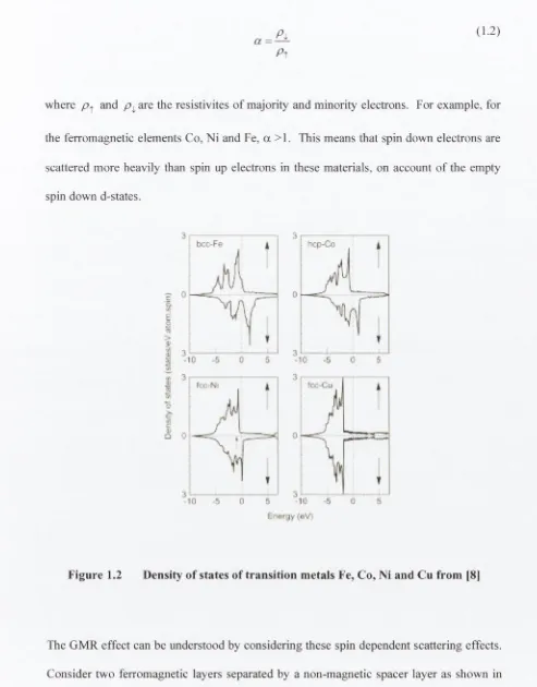
w here and are the resistivites o f m ajority and m inority electrons. For exam ple, for
the ferrom agnetic elem ents Co, N i and Fe, a >1. This m eans that spin down electrons are
scattered m ore heavily than spin up electrons in these m aterials, on account o f the empty spin down d-states.
i
bcc-Fe
0
5 0 5
rcc Ni
3
hcp-Co
n
0 5
& 3
0
3
-10 5 0 5
Eriergy (ftV)
Figure 1.2 Density of states o f transition metals Fe, Co, Ni and Cu from |8|
[image:20.522.17.510.41.671.2]are not scattered in either m agnetic layer and have low resistivity. Similarly, spin down electrons are scattered heavily in both m agnetic layers and have high resistivity. The lower resisitivity o f the spin up channel effectively gives a short circuit and the overall resistance o f the stack is low. In the antiparallel configuration, spin up electrons have low resistivity in one m agnetic layer and high resisitivity in the second layer. Spin down electrons experience the opposite effect so that both types o f electrons are scattered and the overall resistance o f the stack is high. If we assum e that the m ean free paths o f the electrons are larger than the layer thicknesses, then the resistor m odel in Figure 1.3 can be used to describe the situation.
FM NM FM spin FM N M FM
spin spin
Ri Rt Ri Ri
Figure 1.3 Resistor model o f GMR
In the parallel configuration the resistivity is given by:
(1.3)
R^ + R
w h ile in the an tip arallel configuration it is d esc rib ed by:
(1.4)
T h e G M R ra tio is then given by:
A/? Ra f- Rp i \ - a f
R Rp 4or
(1.5)
T his illustrates the im portance o f the scatterin g asy m m etry in the origin o f G M R . S catterin g at in terfaces in m u ltilay e r structures also play s an im p o rtan t ro le and depends on the deg ree o f m atch in g o f the electronic b an d stru ctu res o f the ferrom agnetic an d n o n m ag n etic m ateria ls in the bulk o f the layers and n ea r the interfaces. In o rd e r to obtain a large G M R effect, good electronic structure m atch in g is req u ired fo r one spin direction and bad m atch in g fo r the o ther direction. G ood electro n ic stru ctu re m atch in g explains, in part, the large G M R ratios for F e/C r m ultilay ers w h ere m atch in g is go o d for the m inority electro n s and fo r C o/C u w here good m atch in g o ccurs fo r the m ajority spin electrons [9]
T here are tw o w ay s in w hich the cu rren t can flow th ro u g h a G M R stack; p arallel to the p lan e o f the film or p erp en d icu lar to the plane. T h ese tw o co n fig u ratio n s are kn o w n as cu rren t in p lan e (C IP ) and cu rren t p erp en d icu lar to p lan e (C P P ) (F ig u re 1.4). T he sim ple m odel d iscu ssed above assum es th at the cu rren t d en sities are h o m o g en o u s fo r both spin d irectio n s th ro u g h o u t the layers. T his isn ’t v alid fo r the C IP g eom etry an d is g enerally m ore app licab le to C PP w hich is describ ed in detail by the V alet F ert m odel [10]. T here is a fun d am en tal d iffe ren c e b etw een the im portant length scales in the tw o geom etries. In the case o f C IP G M R , the electric field is uniform alo n g th e in-plane direction. It is im portant then th a t the m ean free path o f the spin up and spin d ow n electrons is m uch larg er than the th ick n esses o f th e layers. T he electrons w ill then, on average, traverse m an y layers
w ithout being scattered as they drift along the in-plane direction and the resistance contributed by each spin channel will be proportional to the scattering rate for each channel. This is the case in Co/Cu m ultilayers for exam ple where the anti ferromagnetic coupling is realized at a Cu layer thickness o f about 0.85 nm and the m ajority m ean free path in Co is around 5nm and Cu is about 30nm [11], In CPP GM R, the electric field created by the current will ensure that electrons are pushed across the non m agnetic spacer tow ards the next m agnetic layer. The im portant length scale here then is the spin diffiision length. This describes the distance an electron can travel w ithout flipping its spin. It is im portant that the spacer layer is thinner than this distance so that electrons retain their spin configurations betw een successive m agnetic scattering events. In addition, because electrons are forced to traverse the interfaces there is an additional spin-dependent interfacial resistance in CPP GM R resulting from the difference in the positions o f the bottom s o f the conduction bands with respect to the Fermi energy in successive layers. CPP G M R is usually m uch higher than CIP GM R. H ow ever applications have generally avoided the CPP geom etry thus far due to the technical challenges o f m aking CPP pillars o f small enough dim ensions such that the resistance is appreciable.
FM
CONTACT NM
FM
CONTACT CONTACT FM NM FM CONTACT
►
CURRENT DIRECTIO NSem i-classical theories have been developed to m odel G M R in m agnetic m ultilayers. The C IP transport properties o f m agnetic m ultilayers are calculated using an adaptation o f the Boltzm ann theory using spin-dependent resistivities o f the m aterials and the spin dependent interfacial resistances as input param eters. These theories have proven successful in explaining m ost o f the general transport trends in m ultilayers and spin valves such as the dependence o f G M R on the thicknesses o f the various layers and also the effects o f specular reflection. A detailed description o f these theories is beyond the scope o f this introduction. A com prehensive review can be found in [12].
M ultilayer systems can have high GM R ratios but are not well suited for applications. The coupling in these m ultilayers oscillates from ferrom agnetic to antiferrom agnetic as a function o f the spacer layer thickness. This thickness is engineered such that the layers are coupled antiferrom agnetically at zero field. This coupling is so strong however, that it takes a rather large m agnetic field (several hundred m T) to overcom e it and get a change in resistance. This is unsuitable in applications such as read head sensors for example, which are exposed to fields o f the order lOmT. A nother disadvantage is the non-linearity o f the resistance change, m aking the m ultilayer system less useful for sensor applications. These constraints led to the developm ent o f the spin valve sensor in 1991 [13] as discussed in the next section.
1.3 Spin valve structures
The basic spin valve elem ent consists o f two m agnetic layers separated by a non-m agnetic spacer. The device is engineered such that the ferrom agnetic layers can be switched from parallel to antiparallel in a controlled and independent m anner. Parallel alignm ent is achieved by the application o f a m agnetic field. A ntiparallel alignm ent can be realized by
several different techniques. Perhaps the m ost obvious m ethod is to use ferrom agnetic layers with different coercive fields. This can be done be using a m agnetically hard and m agnetically soft layer as the ferromagnetic electrodes such as:
NiFe(3nm )/C u(5nm )/Co(3nm )/Cu(5nm ) [14]. These system s are often called pseudo spin valves and an example o f a m agnetisation and m agnetoresistance curve is shown in Figure 1.5. The pseudo spin valve has a symm etric and irreversible response o f the resistance with field. Again, this is a disadvantage for applications in sensors and m agnetoresistive heads. H ow ever pseudo spin valves have been studied for application in G M R M RAM (m agnetic random access m em ory) architecture.
M
MRa
Figure 1.5 Schem atic o f m agnetisation (left) and m agnetoresistance (right) o f a pseudo spin valve
Ta5nm /N iFe3.5nm /C oFel.5nm /C u2.9nm /C oFe2.5nm /IrM nl0nm /T a5nm .
The m agnetisation curve o f this sample consists o f tw o hysteresis loops. At high negative fields both free and pinned layers are aligned parallel with the field. A t close to zero field, the free layer (N iFe3.5/C oFel.5nm ) switches antiparallel to the pinned layer. The pinned layer (CoFe2.5nm ) does not switch until the exchange anisotropy is overcom e at 35m T, the so-called exchange bias field. In the m agnetoresistance curve, at high negative fields both layers are parallel and the resistance is low. At close to zero field the free layer switches sharply to the antiparallel configuration and the resistance reaches a m axim um . As the field is further increased, the pinned layer gradually sw itches and the resistance decreases to the m inimum value.
0.5 -0.0 --0.5 --1.0
--200 -100 0 100 200
w H (m T)
Figure 1.6 M agnetoresistance (top) and m agnetisation (bottom ) o f an exchange biased spin vaive.
1.3.1 Interlayer co u p lin g in spin v a lv e s
The change in the relative orientation betw een the m agnetisation in the free and pinned layers in an exchange biased spin valve does not rely on the existence o f antiferrom agnetic coupling through the spacer. The unidirectional exchange anisotropy o f the pinned layer m eans that the two FM layers sw itch independently. Figure 1.7 shows the reversal o f the free layer. This illustrates the advantage o f the exchange-biased spin valve, w ith high m agnetoresistance and sensitivity at low fields it is ideal for sensor applications. The loop shift in the free layer indicates the presence o f a slight ferrom agnetic coupling through the Cu spacer layer. The three m ain contributions to this coupling are direct coupling through pinholes, Neel or orange-peel coupling and oscillatory RKKY (R uderm an-K ittle-K asuya- Yosida) coupling.
10
8
6
-2
--10 -5 0 5 10
Figure 1.7 Free layer reversal o f a spin valve.
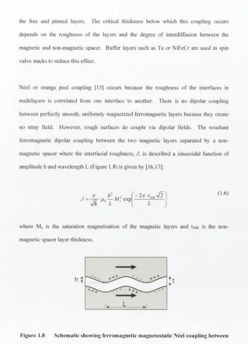
the free and pinned layers. The critical thickness below which this coupling occurs depends on the roughness o f the layers and the degree o f interdiffusion betw een the m agnetic and non-m agnetic spacer. Buffer layers such as Ta or N iFeC r are used in spin valve stacks to reduce this effect.
Neel or orange peel coupling [15] occurs because the roughness o f the interfaces in m ultilayers is correlated from one interface to another. There is no dipolar coupling betw een perfectly smooth, uniformly m agnetized ferrom agnetic layers because they create no stray field. However, rough surfaces do couple via dipolar fields. The resultant ferrom agnetic dipolar coupling betw een the two m agnetic layers separated by a non m agnetic spacer where the interfacial roughness, J, is described a sinusoidal function o f am plitude h and w avelength L (Figure 1.8) is given by [16,17]:
1 ^ * ^ 2
V8
(1.6)
w here Ms is the saturation m agnetisation o f the m agnetic layers and tNM is the non m agnetic spacer layer thickness.
hi
Figure 1.8 Schem atic showing ferrom agnetic m agnetostatic Neel coupling between two ferrom agnetic layers separated by a non-m agnetic spacer.
[image:28.528.22.516.29.712.2]As m entioned in section 1.2, the exchange coupling in m ultilayer systems such as (Co/Cu)n oscillates from ferrom agnetic to antiferrom agnetic w ith the spacer layer thickness. This is
the sam e as the RKKY coupling m echanism w hich describes the interaction between ferrom agnetic im purities in a non-m agnetic m atrix [18]. This effect is pronounced in high quality m ultilayers. It has been shown that the G M R ratio also oscillates as a function o f
spacer thickness in these system s and the thickness o f the N M layer can be chosen to coincide with antiferrom agnetic coupling at zero field and high G M R [19]. In spin valves with only two m agnetic layers separated by a non-m agnetic spacer, an oscillation o f the
coupling as a function o f the spacer thickness can be seen in high quality samples w ith low roughness. As the roughness increases the coupling becom es ferrom agnetic as Neel coupling dom inates [20], Optim isation o f the spin valve coupling m echanism s through optim isation o f roughness and spacer layer thickness can therefore be used to adjust the offset o f the free layer sw itching or the bias point. This is important from an applications point o f view.
1.4 Exchange bias
In 1956 M eiklejohn and Bean discovered the phenom enon o f exchange anisotropy when studying ferrom agnetic Co particles em bedded in their native antiferrom agnetic oxide CoO [21,22]. W hen the particles were cooled in a m agnetic field from room tem perature, where
the CoO is param agnetic, to 77K where it is antiferrom agnetic, a unidirectional anisotropy appeared. The same treatm ent carried out on non-oxidised Co particles resulted in uniaxial
anisotropy (Figure 1.9). This unidirectional anisotropy was attributed to exchange interaction between the AFM CoO particles and the FM Co core and w as term ed exchange anisotropy. The m ost notable m anifestation o f this phenom enon was the shift from zero
Since then, exchange anisotropy has been observed in a w ide variety o f system s containing
FM -AFM interfaces. A review o f the experim ental findings is given in [23], The com m on
features are the shift from zero field o f the m agnetisation curve by an am ount know n as the
exchange bias field Hex, an enhanced coercivity, and the disappearance o f these features at
tem peratures above Tb, the blocking tem perature o f the AFM w here Tb < Tn, the Neel
tem perature o f the AFM.
35 30 25^ 20
[ / H tM U L T IP L Y BY IQ 3 )
25 30 35
Figure 1.9 Hysteresis o f Co/CoO particles m easured at 77 K after cooling under a m agnetic field o f 1 T (1) and zero field (2) |22).
M eiklejohn and Bean explained the unidirectional anisotropy and exchange bias by
considering a simple picture o f the FM /AFM interface (Figure 1.10). In this case there is a
ferrom agnetic interaction at the interface and the m agnetisations are aligned. The interface
is non-com pensated, i.e. only one type o f antiferrom agnetic spin is present at the interface
and the m agnetisation at the interface is non-zero. The interaction betw een at the
FM /A FM interface tries to keep the m agnetisations at the interface aligned and can be
thought o f as an effective field acting on the FM film. It is m ore energetically favourable
for the FM to be aligned along the direction o f this effective field. During the hysteresis cycle, w hen the applied field is as shown in Figure 1.10, the FM spins rem ain aligned with the AFM until the applied field is greater than the sum o f the effective field and the coercive field o f the FM. In the second h a lf o f the hysteresis cycle, the applied field is now in the direction o f the effective field and the FM will switch at a lower applied field value given by the difference betw een coercive field o f the FM and the effective field. So the FM has only one stable configuration, as shown by unidirectional anisotropy and a shift from zero o f the hysteresis cycle by a value corresponding to the exchange bias field, Hex.
Figure 1.10 Phenom enological description o f exchange bias
E = - H M c o s e + K ^ ^ AFM^AFM s i n^ 6 > - J C O S 6 > ( 1 - 7 )
The angle 9 is m ade betw een the m agnetisations o f the FM and AFM layers and their
respective anisotropy axes, which are collinear. The first term is the Zeem an energy, describing the interaction betw een the applied field and the m agnetisation o f the FM. The second and third term s represent the anisotropy energies o f the FM and AFM films. The final term represents the interaction betw een the tw o films where J is the interface exchange coupling constant. I f we assum e that the antiferrom agnet is rigid the energy sim plifies to:
E = - H M p^tpf^cos,9+ K ,,^ e - J COS0 (
1
•8
)M inim ising the energy w .r.t 9 gives two extrem a for the direction o f the m agnetisation o f
the FM film when 9 = 0 and 9 = 7t. Stability o f the 0 = 0 configuration is possible if
J I + H M + 2 K y ^ >Q&nd stability o f the 0 = ti configuration is possible
> 0.
This corresponds to the coercive fields:
2K,^tp^+J
( 1.9)^ C \ ~
^ F M^ F M
M F M^ F Mt
(1.10)
As the tw o coercive fields are not equal in m agnitude, the hysteresis cycle is shifted by the bias field given by:
J (1.11)
= ■
^ F M^ F M
The dependence o f the exchange field on 1/tpM underlines the interfacial nature o f the phenom enon and has been verified experim entally on several systems. However, the
exchange fields estim ated from equation (1.11) are orders o f m agnitude larger than those reported experim entally, if J is supposed to be sim ilar to the bulk exchange constant [24]. Several other m odels sum m arized in [23] and [25] have been form ulated to account for
different important param eters in exchange biased system s, w hich are not taken into account in the basic M eiklejohn and Bean approach. The m ain lim itation o f this m odel is in considering that both the AFM and FM are perfectly uniform and single dom ain as it is
unlikely that this effectively describes the low est energy m agnetic configuration near the interface. It is also assum ed that the spin structure in the AFM layer rem ains fixed as the FM layer switches. An alternative m odel taking these lim itations into account was proposed by Mauri in 1987 in allow ing a dom ain wall to develop parallel to the interface in the AFM film during the FM reversal [26]. He assum ed that the coupling at the interface betw een FM and AFM m om ents is ferrom agnetic and the m om ents o f the FM and AFM films are parallel at the surface in the absence o f an applied field, the thickness o f the FM film is sm aller than the domain wall width and the FM is therefore considered single
domain. The AFM is considered infinite and a dom ain wall is allowed to develop in the AFM during reversal o f the FM. In order for the dom ain wall to form, its energy
m ust be less than the interfacial coupling energy J. M inim ization o f the
system energy in this case gives an exchange field of:
„ (1-12)
This m eans the exchange field is reduced by a factor J I and gives values for
ferrom agnetic film and an antiferrom agnetic film o f infinite thickness. It assum es the interface plane is hom ogenous and that the AFM m om ents at the interfaces are non com pensated. A com pensated interface is one with an equal distribution o f the tw o AFM sublattices at the interface. The ferrom agnet is then exchange coupled equally to both sublattices and there is no net m om ent for the ferrom agnetic to interact with. The previous m odels predict zero exchange field for this scenario but experim ental studies show that this is not the case. A m odel by Koon [27] predicts the form ation o f dom ains in the AFM parallel to the interface in a sim ilar m anner to Mauri except that the interface can be com pensated or non-com pensated. The draw back is that the m odel assum es uniform properties at the interface. The M alozem off m odel [28, 29, 30] has addressed this situation by considering that an ideal interface is unrealistic and that roughness leading to m agnetic defects gives rise to local random fields. The total energy o f the antiferrom agnet, including the contribution from the random fields, is then m inim ized by the form ation of dom ain walls perpendicular to the interface. The contribution o f energy difference betw een the different random domains produces the exchange bias.
More recent experim ental findings [31,32] support an extension o f the M eiklejohn and Bean m odel by the discovery using x-ray m agnetic circular dichroism (X M CD ) that only a small fraction o f AFM spins are pinned at the interface. These pinned spins do not rotate in an external m agnetic field and the coupling betw een them and the spins in the FM layer results in the exchange bias and the shift o f the hysteresis loop. The m ajority o f the uncom pensated interfacial spins, however, are not pinned. These spins are dragged along with the m agnetisation reversal process in the FM layer and although they do contribute to an enhanced coercivity, they are not responsible for the exchange bias effect. Taking into account that only a small pinned fraction p o f the uncom pensated interfacial m om ents
contributes to the bias, the M eiklejohn and Bean m odel (1.11) can be written as [31]:
ex
^ fmK
where J ^ = p j
This eliminates the discrepancy between the values o f J predicted by the Meiklejohn and Bean model and those measured experimentally.
All o f these models and many more have found different degrees o f agreement with the vast range o f existing experimental results on exchange anisotropy. A fiilly comprehensive model o f exchange bias is still lacking and there remain several unsolved issues. It seems the detailed mechanism o f exchange bias may be quite different for each specific FM/AFM system. Nevertheless it is a phenomenon which has been implemented very successfully in several devices. The technological considerations in tailoring exchange bias for applications are well studied and will be discussed briefly in the next section.
1.4.1 Exchange bias materials and properties
The choice and study o f antiferromagnets for spin valves has been largely driven by the requirements o f read head applications. The main requirements are as follows:
■ Large exchange bias field
■ High resistivity in order to reduce parasitic shunting o f resistance in CIP geometry ■ Low processing temperature so that the structural integrity o f the rest o f the stack is not
affected during deposition or post deposition anneal ■ Corrosion resistance
■ Low critical thickness - the m inimum thickness o f antiferrom agnetic m aterial for which exchange bias can be established.
The m ost com m only studied antiferrom agnetic layers are m anganese-based alloys such as FeM n, IrM n, NiM n, PdMn and PtMn. FeM n was for a long time the m ost intensively
studied alloy. Film s o f com position Fei.xMnx with x ~ 0.5 were im plem ented in some o f the first spin valves [13]. Further studies indicated a low blocking tem perature in the range
140 to 190 °C rendering the m aterial unsuitable for disk-drive applications [33]. Other disadvantages include low stability with respect to Mn diffusion and poor corrosion resistance [34], Iri.xMnx with x ~ 0.8 has been intensively studied since its introduction as
an exchange bias m aterial in 1996 [35] and is the m aterial used in spin valves discussed in this work. One o f its advantages is ease o f processing. For spin valves in which the IrMn is grown on top o f the FM layer (top spin valves), room tem perature deposition in a small m agnetic field is enough to establish reasonable exchange bias. For spin valves in which the IrMn is grown beneath the FM layer (bottom spin valves), a m agnetic anneal is
norm ally required although a small exchange bias at room tem perature can be obtained. A detailed discussion o f the effects o f m agnetic annealing on top and bottom IrMn spin valves is presented in Chapter 4. The advantages o f IrMn over FeM n include higher blocking tem perature, larger exchange field, lower critical thickness, higher resistivity and
better stability against Mn diffusion [34, 38].
NiM n, PtM n and PdM n are ordered AFM com pounds with very high Neel tem peratures ranging from 540°C for PdM n to 800°C for NiM n. This m akes them good candidates for
application as exchange bias materials. U nfortunately in the as-deposited state these m aterials are random alloys with low exchange bias and a long annealing process is required to induce a phase transform ation to the ordered state. In the case o f NiM n, for
exam ple, an n ealin g pro cesses from 10-40 h o u rs at tem p eratu res aro u n d 280 °C h av e been
re p o rted [36], N ev erth eless, these m aterials h av e very h ig h b lo ck in g tem p eratu res and
ex c ellen t therm al stability [37,38], w hich m ak es th em v ery suitable fo r use in spin valves
for read h ead applications.
O xide antiferro m ag n ets, such as N iO and a - F e2 0 3 h av e also been im p lem en ted in spin
valv es [39,40]. T he o bvious advantage o f an o xide an tife rro m ag n e t is the elim in a tio n o f
cu rren t shunting though the layer due to its intrinsically high resistivity. A n added
adv an tag e o f increased G M R ratio due to sp ec u la r re flectio n at the oxide interface w as
d isco v ered w hen studying N iO spin valves. T his has re su lted in high G M R ratios o f u p to
28 % [41]. U nfortunately both N iO and a - F c203 su ffe r from low ex c hange b ias fields and
large critical thicknesses. An overview o f the m ain p ro p e rtie s o f the an tife rro m ag n e ts used
in spin valves from [42, 44] is given in T able 1.1.
A FM F ilm s FeM n IrM n N iM n P tM n N iO a - F c2 0 3 C ritical thickness, tc
(nm ) 7 - 1 0 5 - 8 25 1 0 - 1 5 50 50
N eel T em p, Tn (°C ) 230 420 800 702 250 680
B lock in g tem p, Tb
(°C ) 140-190 240-290 3 6 0-400 350-400 180-230 250
E x ch an g e energy, J (m J/m ^)
0.10-0.15
0.12-0.40
0.30-0.40
0.20-0.30
0.02-0.12
0.03-0.12
Table 1.1 Characteristics of different types of antiferromagnets. Values of
1.5 Spin valve designs
Im provem ents in spin v a lv e perform ance (G M R , e x c h a n g e field , sen sitiv ity ) are
co n tin u a lly pursued both through the d e v elo p m en t o f n e w m aterials and the d esig n o f n ew spin v a lv e g eo m etries. T he b asic F M /N M /F M /A F spin v a lv e has e v o lv e d into m any
variants [43, 4 4 ].
T he standard spin v a lv e is co m p o se d o f at least six layers; buffer layer, free layer, spacer layer, p in n ed layer, antiferrom agnetic layer and cap p in g layer. T he bu ffer layer is u sually
2 -5 nm o f Ta and is u sed to increase the quality o f the sub seq u en t layers and reduce
rou gh n ess. The rela tiv ely high resistiv ity (p = 160 x 10'* Q m ) o f tantalum m ak es it a
su itab le ch o ic e as shunting e ffe c ts through it are n e g lig ib le . The cap p in g layer is also u su ally Ta and protects the structure from ox id a tio n and corrosion . T he free layer in ex ch a n g e b iased spin v a lv e s gen erally c o n sists o f tw o ferrom agn etically co u p led layers w ith different co m p o sitio n s. The m ost frequently u sed com b in ation is NigoFe2o/Co9oFeio. The p erm alloy layer is used to reduce the co e r c iv ity w h ereas the C oF e g iv e s a higher M R ratio d u e to the larger scattering potential for m in ority electron s at the C oF e/C u interface. U su a lly the antiferrom agnetic layer is at the top o f the spin v a lv e structure, h en ce the nam e
top spin v a lv e . The antiferrom agnet can a lso be gro w n at the bottom o f the stack - a bottom spin v a lv e. T he bottom spin v a lv e is m ore d iffic u lt to rea lize exp erim en tally as the
structure gen erally n eed s to b e annealed in a m a g n etic field to estab lish reasonable e x c h a n g e bias. T yp ical M R valu es for top and bottom spin v a lv e s w ith IrMn range from 5
- 10% .
Dual spin valves consist o f essentially three FM layers separated by two non-m agnetic
spacers. The m agnetisation o f the outer two FM layers are pinned by an AFM layer,
w hereas the inner FM layer is free. An exam ple o f a dual spin valve structure is
N iO /C o/Cu/Co/Cu/CoN iO . GM R ratios as large as 24.8% [45,46] have been reported for
these spin valves but the increased thickness o f the structure can m ake it unsuitable for
read head applications.
A further advance in spin valve design was the developm ent o f the synthetic
antiferrom agnet (SAF). The SAF is a three-layer stack consisting o f two ferromagnetic
layers (usually Co or CoFe) separated by a thin layer o f non-m agnetic spacer (usually Ru).
The coupling betw een the ferrom agnetic layers oscillates betw een ferrom agnetic and
antiferrom agnetic as a function o f the Ru thickness and is strongly antiferrom agnetic in the
range 0.5-1.0 nm [47]. One o f the ferrom agnetic layers in the SAF is coupled to an
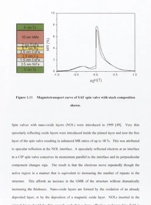
antiferrom agnet to give a spin valve o f the form shown in Figure 1.11. The antiparallel
coupling across the Ru layer is m uch stronger than the interfacial coupling between the
FM /AFM layer and the two FM layers in the SAF rem ain antiparallel up to quite large
fields. The m agnetoresistance curve in Figure 1.11 shows that the pinning fields in the
SAF spin valve can be twice as large as that o f the standard spin valve and the G M R value
is the same. A nother advantage o f using the SAF is that, in a patterned device, stray field
created by the pinned layer on the sensing layer is reduced because o f the antiparallel
alignm ent o f the tw o FM layers in the pinned layer. An analytical calculation o f the
5 n mT a
1 0 nm IrMn
2 nm C Q Fe~ 0 . 7 nm R ~ 2 . 5 nm C o F e 2 . 9 nm Cu 1. 5 nm C o F e
3 . 5 nm MiPe
5 n mTa
8
6
4
2
0
-1.0 -0.5 0.0 0.5 1.0
M-oH( T )
Figure 1.11 Magnetotransport curve o f SAF spin valve with stack composition
shown.
Spin valves with nano-oxide layers (NOL) w ere introduced in 1999 [49]. Very thin specularly reflecting oxide layers were introduced inside the pinned layer and near the free layer o f the spin valve resulting in enhanced M R ratios o f up to 18 %. This was attributed
to specular reflection at the NOL interface. A specularly reflected electron at an interface in a CIP spin valve conserves its m omentum parallel to the interface and its perpendicular
com ponent changes sign. The result is that the electrons m ove repeatedly though the active region in a m anner that is equivalent to increasing the num ber o f repeats in the
structure. This affords an increase in the G M R o f the structure w ithout dram atically increasing the thickness. N ano-oxide layers are form ed by the oxidation o f an already
[image:40.522.17.511.33.703.2]a lso been reported in spin v a lv e s w ith o x id e antiferrom agnets such as N iO [46] and a -F e2 0 3 [51], N O L insertion into a spin v a lv e w ith a m eta llic antiferrom agnet such as IrMn can b e m ore u sefu l due to the high er therm al stab ility and lo w er critical th ick n ess o f the antiferrom agnet.
Spin filter spin v a lv e s have the structure A F M /F M /N M /F M /B w h ere B is a con d u ctiv e n o n -m a g n etic back layer. The result is an increased m ean free path and reduced resistan ce for m ajority spin electron s in parallel align m en t and h en ce an increased G M R ratio [52], O ptim isation is a trade o f f b etw een the increased m ean free path and increased current sh u n tin g through the back layer. The advantage o f the spin filter spin v a lv e is that the th ick n ess o f the free layer can be reduced to le v e ls that w o u ld be sub-optim al w ith ou t a back layer. A thinner free layer is ad van tageou s for read head applications as the con tin u ed reduction in the bit siz e o f m agn etic record in g heads m ean s sm aller m agn etic flu x co m in g from each bit. T his m ean s that the m o m en t o f the free layer m ust be d ecreased in order to m aintain the sam e am plitude o f rotation.
1.6
Spin valves devices
Spin v a lv e s are currently used in a w id e variety o f com m ercia l sen sor products. The m ain ap p lication s at present are in read heads o f hard d isk drives in the m agn etic storage industry and as m agn etic field sen sors. The p recise requirem ents o f a spin v a lv e sen sor and its advantages over other typ es o f sen so r d ep en d on the sp e c ific application. The general requirem ents for a spin v a lv e sen sor are as fo llo w s [53]:
■ Small hysteresis ■ Low noise ■ Thermal stability
■ Good repeatability and reliability
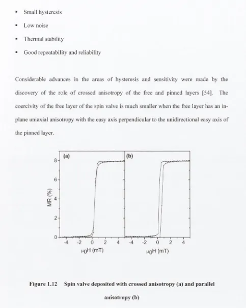
Considerable advances in the areas o f hysteresis and sensitivity were m ade by the discovery o f the role o f crossed anisotropy o f the free and pinned layers [54], The coercivity o f the free layer o f the spin valve is m uch sm aller when the free layer has an in plane uniaxial anisotropy with the easy axis perpendicular to the unidirectional easy axis o f the pinned layer.
8
6
4
2
-2 0
0
■4 2 4 ■4 2 0 2 4
MqH ^qH (mT)
Figure 1.12 Spin valve deposited with crossed anisotropy (a) and parallel
anisotropy (b)
In such system s with crossed-anisotropies when the external field is applied parallel to the biasing direction, the m agnetisation o f the free layer switches by coherent rotation
[image:42.522.24.507.46.649.2]resulting in a near linear variation o f the resistance with field. In contrast, in the case o f parallel anisotropies, m agnetisation reversal is the result o f dom ain wall m ovem ent leading to hysteresis in the M R curve. As a result, strong Barkhausen noise is superim posed on the sensor output signal due to pinning and depinning o f dom ain walls. In Figure 1.12, a spin valve with free layer N iFe(3.5nm )/C oFe(I.2nm ) and pinned layer CoFe (2.5nm )/IrM n (lO nm ) is shown with crossed (a) and parallel (b) anisotropy. The crossed configuration w as obtained by growth o f the spin valve in a m agnetic field and rotation o f the sam ple by 90 degrees for growth o f the pinned layer.
The crossed anisotropy configuration is used in applications w here a linear, reversible, hysteresis-free output is required. These applications include read-heads for m agnetic recording and m agnetic field sensors. The hysteretic, irreversible sw itching o f the parallel anisotropy configuration is useful when the spin valve is to be applied as a m em ory elem ent in GM R M RAM for exam ple where two zero field states o f the free layer are required to represent a digital “0” and “ 1” .
1.6.1 Spin valves as magnetic-field sensors
m agn etic fie ld and the output v o lta g e . M in im ization o f the n o ise and particularly the m agn etic n o ise is essen tia l for spin v a lv e sen sors. T h is can b e a ch ie v ed by appropriate
d esig n o f the sen so r g eom etry. The op tim isation o f sp in v a lv e s for m agn etic field sen sors is d escrib ed in detail in chapter 6.
1.6.2 Spin valves in read heads
A n o v e rw h e lm in g am ount o f spin v a lv e research has b een driven by the interests o f the m agn etic storage industry. T he first m agn etic d isk drive, introduced by IBM in the early
1 9 5 0 ’s, w a s term ed R A M A C and had an areal d en sity o f 2 kb/in^ [55]. T he areal d en sity o f this drive, based on in d u ctive tec h n o lo g y , ex p erien ce d a grow th rate o f 3 0 % /year until 1992 w h en m agn etoresistive heads b ased on the anisotropic m agn etoresistan ce o f p erm alloy film s w ere introduced. From this poin t on the areal d en sity increased at a rate o f 6 0 % /year b o o sted by the d isc o v ery o f G M R and the im plem entation o f spin v a lv e s in read heads in 1998. T od ay, areal d en sities o f up to 100 Gb/in^ h a v e b een dem onstrated.
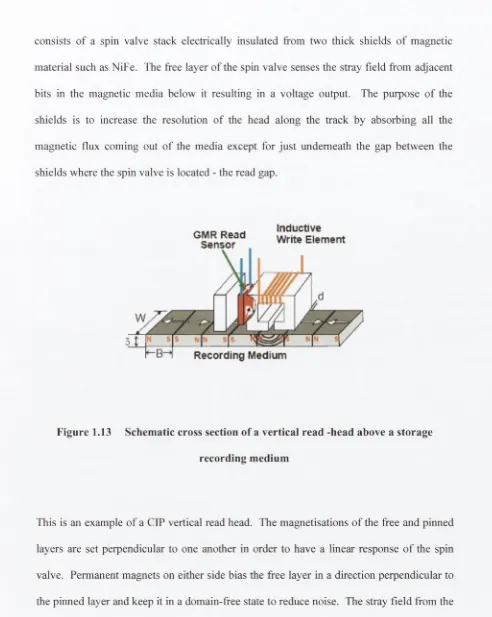
T he p rinciple o f m agn etic recorded is illustrated sch em a tica lly in Figure 1.13. T h e b asic co m p o n en ts are the record in g m ed ia and a read-w rite head. T he record in g m ed iu m is a
disk o f m agn etic m aterial on w h ich inform ation is stored as abrupt c h a n g es in m agn etisation , or m agn etic bits in tracks a lo n g the disk. The areal d en sity is then the
product o f the d en sity at w h ich transitions can be p ack ed a lo n g a track (the linear bit d en sity ) and the d en sity at w h ich tracks can b e p ack ed together (th e track d en sity ). T he
read-w rite head is p o sitio n ed on an air bearing slid er (A B S ) at a fix e d p o sitio n a b o v e the disk. The writer is e ssen tia lly a subm icron electrom agn et, the stray field from w h ic h is used to sw itch the m agn etisation o f bits on the recording m edia. T h e h igh er the saturation
m agn etisation o f the p o le p ie c e s o f the writer, the high er the w rite field . M aterials
currently u sed in w rite heads are NigoFe2o, N i4 5F es5 and F eT aN . T he reader currently
consists o f a spin valve stack electrically insulated from two thick shields o f m agnetic
m aterial such as NiFe. The free layer o f the spin valve senses the stray field from adjacent
bits in the m agnetic m edia below it resulting in a voltage output. The purpose o f the
shields is to increase the resolution o f the head along the track by absorbing all the
m agnetic flux com ing out o f the m edia except for ju st underneath the gap betw een the
shields where the spin valve is located - the read gap.
Figure 1.13 Schematic cross section of a vertical read -head above a storage
recording medium
This is an example o f a CIP vertical read head. The m agnetisations o f the free and pinned
layers are set perpendicular to one another in order to have a linear response o f the spin
valve. Perm anent m agnets on either side bias the free layer in a direction perpendicular to
the pinned layer and keep it in a dom ain-free state to reduce noise. The stray field from the
recording m edium is then in a direction perpendicular to the free layer and causes it to
rotate coherently resulting in a linear response. This linear response can be com prom ised
and offset from zero in a sim ilar m anner to blank spin valves as discussed in section 1.3.1.
The interlayer coupling tries to align the free and pinned layers ferrom agnetically. Other
GMR Read Sensor
Inductive Write Element
[image:45.522.19.511.28.645.2]forces include antiferrom agnetic coupling with the dipolar field created by the pinned layer
m agnetisation which becom es im portant at sm aller dim ensions. The Oersted field created
by the sense current in the spin valve also has an affect on the free layer. These fields can
be adjusted in order to reduce the offset by optim isation o f process and m easurem ent
param eters. The coupling betw een the layers can be reduced by appropriate choice o f
spacer layer thickness. The effect o f the dipolar field o f the pinned layer can be almost
elim inated by use o f a synthetic antiferrom agnet as discussed in section 1.5 and the sense
current can be changed to adjust the Oersted field. In practice a com bination o f these
techniques is used.
An im portant param eter in the perform ance o f read heads is the readout resolution parallel
and perpendicular to the trackwidth o f the recording medium. The resolution parallel to
the trackw idth is determ ined by the effective length o f the spin valve and is determ ined by
the spacing betw een the leads, the position o f the perm anent m agnets and is generally
lim ited by the resolution o f lithographic techniques. The resolution perpendicular to the
trackw idth is determ ined by the read-gap w hich is determ ined by the com bined thickness
o f the insulating layers and the spin valve stack. Reduction o f the insulation thickness
risks shortage and increased vulnerability to electrostatic discharge. M ethods o f reduction
o f the spin valve thickness through specular reflection and highly conductive layers have
been investigated as discussed in section 1.5 but only small im provem ents can be foreseen.
For this reason and several other advantages, m ore efforts are now focussed on CPP MR
heads based on spin valves or tunnel junctions. In the CPP configuration the shields can
double as current leads to the MR elem ent and the need for the insulation layers is
elim inated resulting in an im m ediate reduction o f the read-gap and increased lateral
resolution.
1.6.3 Spin v a lv e s in M R A M
Existing sem iconductor random access m em ories such as SRAM (static random access
m em ory) and DRAM (dynam ic random access m em ory) are disadvantaged by their
volatility [56], M agnetic random access m em ory (M R A M ) has the potential advantages o f
non-volatility, speed, unlim ited write endurance and low cost. M RAM has been the
subject o f intense research over the last ten to fifteen years. Initial M RAM architecture
was based on the A M R o f N iFe elem ents but soon m oved on to G M R m ultilayers and then
spin valve structures. M RAM based on exchange bias spin valves have been dem onstrated
[57] but m ost w ork on GM R M RAM has been based on pseudo spin valve cells [56], In
the G M R-M RA M architecture, the spin valve elem ents are organised in a square array.
Each spin valve elem ent is located at a cross point betw een two sets o f perpendicular lines,
w ord lines and sense lines. Information is stored as the orientation o f the m agnetisation o f
the hard layer o f the spin valve. In order to write inform ation in a cell, pulses o f current
are sim ultaneously sent in the sense and w ord lines that cross at the selected cell. These
currents generate two perpendicular m agnetic fields on the hard layer (one along its easy
axis and one along its hard axis) and can switch its m agnetisation direction. The other spin
valve cells experience either no field or one o f the fields, i.e. are “h a lf selected” . Only the
cell w hich experiences both fields switches. The read process is perform ed by passing a
current through the sense line to orient the m agnetisation o f the free layer and then reading
the resistance. Since the cells are connected in series, a differential tw o-step read out
process m ust be perform ed. This slows down the read tim e. O ther lim itations include low
output signals and the unsuitability for scaling to high densities. The discovery o f
magnetic tunnel junctions (M TJs) offered the possibility o f m uch higher signals and read
times. Present research on M RAM focuses entirely on architectures based on magnefic