SEPT, Vol. I, ISSUE-II www.srjis.com Page 394 POSSIBILITY OF CONSTRUCTING ELECTRONIC DEVICES WITH
DIMENSIONS ON THE NANOMETER SCALE
Gautam S. Ughade1, Madhav N. Rode2, Ph.D. & Vilas Patil3 1
At Jaigaon, Post Sirsala Tq- Parli (V), Dist-Beed 431128
2
Dept. of Physics Vaidyanath College, Parli Vai., Pin - Ta. Parli-Vai., Dist: - Beed 431515
3
A/p Kodoli (Rokhade Galli) Tal Panhala, Dist- Kolhapur.
This study reviews research developments aimed at the design of electronic computers that contain components with dimensions of only a few nanometers. A nanometer, one billionth of meter, is only about 10 atomic diameters. Such nanometer scale electronic computers {i.e., electronic nanocomputers"{that contain molecular-scale components are likely to be up to 10,000 times more densely integrated than today's smallest microcomputers. Electronic technology is one of several alternative technologies (e.g., mechanical, chemical, quantum) that have been proposed for implementing a nanocomputer. Electronic technology for nanometer-scale computers has the advantage, though, that it builds upon nearly a half century of experience and infrastructure developed for electronic computing. Electronic nanocomputers could be orders of magnitude faster than current electronic computers, as well as many times smaller or more densely integrated.
1. Introduction
For the past forty years, electronic computers have grown more powerful as their basic
subunit, the transistor, has shrunk. However, the laws of quantum mechanics and the
limitations of fabrication techniques soon will prevent further reduction in the minimum size
of today's semiconductor transistors. Researchers have projected that once the smallest
features of the transistor's design shrink to less than 0.1 micrometers (or microns, millionths
of a meter), the devices no longer will function usefully In order to continue this
miniaturization down to the molecular scale, present-day microelectronic device designs must
be replaced with new designs that take advantage of the quantum mechanical effects that
dominate on such a small scale.
There are a number of obstacles to making molecular scale electronic computer devices.
What will they look" like? Upon what operating principles will they function? How will
individual devices be connected together? Once designed, how will these computers be
SEPT, Vol. I, ISSUE-II www.srjis.com Page 395
research on the design of electronic computers integrated on the molecular scale. The authors
have attempted to articulate a vision of future directions for the field based upon present
developments. This vision and the answers to the questions above are presented in
nonmathematical terms intended for a general, technically interested readership. However,
this review article builds upon several, more technical and more specialized overviews and
treatises that have preceded the present effort.
Fig.1: Genesis of Nanotechnology
Molecular-scale electronic devices will measure less than 100 nanometers on a side. One
nanometer (one billionth of a meter) is a linear distance spanning approximately ten atomic
diameters. By way of comparison, the smallest features on today's commercially available,
state-of-the-art integrated circuits have linear dimensions of about three hundred fifty
nanometers (0.35 microns) [50,284]. If a transistor could be made with a 1 nanometer
minimum feature size (the dimension of the smallest feature on a device), over 10,000 of
such nanodevices" would ¯t into the same area as a present day transistor. In other words, an
electronic computer made of such nanometer-scale components{i.e., a nanocomputer"{could
be many orders of magnitude more powerful than today's microcomputers.
2. Nanoelectronic Two-State Devices
Electronic nanocomputers could possess the advantages of high speed and low power
consumption. Such features would make them technically and economically desirable for a
new range of applications. This potential has been an enormous stimulus to research and
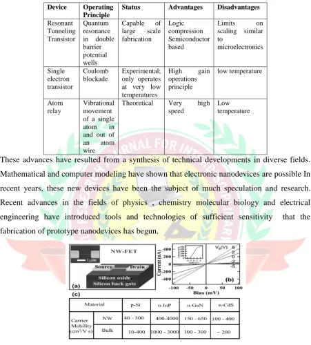
SEPT, Vol. I, ISSUE-II www.srjis.com Page 396 Table 1: Summary of Nanoelectronic Two-State Devices
Device Operating
Principle
Status Advantages Disadvantages
Resonant Tunneling Transistor
Quantum resonance in double barrier potential wells
Capable of
large scale
fabrication
Logic compression Semiconductor based
Limits on
scaling similar to microelectronics Single electron transistor Coulomb blockade Experimental; only operates at very low temperatures
High gain
operations principle low temperature Atom relay Vibrational movement of a single
atom in
and out of
an atom
wire
Theoretical Very high
speed
Low temperature
These advances have resulted from a synthesis of technical developments in diverse fields.
Mathematical and computer modeling have shown that electronic nanodevices are possible In
recent years, these new devices have been the subject of much speculation and research.
Recent advances in the fields of physics , chemistry molecular biology and electrical
engineering have introduced tools and technologies of sufficient sensitivity that the
fabrication of prototype nanodevices has begun.
Fig. 2 Nanowire electronic properties
The basic electronic properties of NWs can be characterized using electrical transport studies
in a nanowire field effect transistor (NW-FET) configuration. The NW-FETs are prepared by
dispersing a suspension of NWs in ethanol onto the surface of an oxidized silicon substrate,
where the underlying conducting silicon is used as a global back gate. Source and drain
electrodes are defined by electron beam lithography followed by electron beam evaporation
of metal contacts, and electrical transport measurements are done at room temperature.
SEPT, Vol. I, ISSUE-II www.srjis.com Page 397
FET to characterize its electrical properties. Gate sweeping measurement of the
NW-FET enables elucidation of important qualitative and quantitative properties of NWs. For
example, changes in Vg produce variations in the electrostatic potential of the NW, and hence
modulate the carrier concentration and conductance of the NW. Depending on the
conductance modulation, it is possible to determine the doping type and estimate the carrier
mobility in individual NWs using standard transistor formula: dI/dVg = μ(C/L2)Vsd and C ≅
2πεε0L/ln(2h/r), where μ is the carrier mobility, C is the capacitance, ε is dielectric constant,
h is the thickness of the SiO2 dielectric, L is the length, and r is radius of the NW [42]. In this
way, we have characterized a broad range of NW materials including p-type Si, n-type GaN,
CdS, and InP NWs. In all cases, the NW materials show excellent carrier mobility
comparable to bulk materials which demonstrates the high quality of these materials.
3. Objectives
The main objective of this study is the development of theoretical and experimental methods
for the controlled manipulation of surfaces at the nanometer scale, including the design,
construction and experimental demonstration of an atomic force microscope (AFM) based
manipulator. Different experimental and control techniques have been combined in the
NanoManipulator system to optimize AFM lithography. Optical video microscopy allows a
fast recognition of the sample and exact positioning of the AFM tip in the particular region of
interest, while UV-laser ablation offers the possibility of noncontact manipulation of a wide
range of materials, including biological specimens.
4. Hypotheses
Self-assembly techniques that allow the controlled growth of nanometer-scale organic
molecular films present new opportunities to develop electronic devices with dimensions
much smaller than those of current technologies. In this thesis we address several of the
challenges to realizing this goal, and demonstrate a molecular-scale programmable-resistance
memory device.
Although technologically attractive, field-effect transistors (FETs) with a self-assembled
organic channel are difficult to realize due to the poor gate-channel coupling. We have used
electrostatic modeling to determine guidelines that allow the maximum gate modulation of
the channel potential in these devices.
5. Conclusion
The rapid miniaturization of electronics to the submicron scale has led to remarkable
SEPT, Vol. I, ISSUE-II www.srjis.com Page 398
the microelectronic industry advances toward ever smaller devices, it is believed that both
physical and economic factors of current top-down silicon technology will soon limit further
advances. To go beyond these limits and fuel the expected demands of future society will
require revolutionary breakthroughs rather than current evolutionary progress. In general
terms, bottom-up assembled nanoscale electronics could provide unparalleled speed, storage,
and size reductions and hold the promise of powering future electronic devices that can
outperform existing devices and open up totally new opportunities. To enable integrated
nanoelectronics will require conceptually new device building blocks, scalable circuit
architectures, and fundamentally different fabrication strategies. A bottom-up approach,
where functional electronic structures are assembled from chemically synthesized,
well-defined nanoscale building-blocks, has the potential to go far beyond the limits of top-down
technology by defining key nanometer-scale metrics through chemical synthesis and
subsequent assembly not by lithography.
References
C. Thelander, P. Agarwal, S. Brongersma, J. Eymery, L. F. Feiner, A. Forchel, M. Scheffler, W. Riess,
B. J. Ohlsson, U. Gösele and L. Samuelson, Mater. Today, 2006, 9,28
K. A. Dick, Prog. Cryst. Growth Char. Mater., 2008, 54, 138
J. D. Meindl, Q. Chen, J. A. Davis. Science 293, 2044 (2001).
C. M. Lieber. Sci. Am. Sept., 58 (2001). C. M. Lieber. MRS Bull. July, 486 (2003).
X. Duan, Y. Huang, Y. Cui, C. M. Lieber. In Molecular Nanoelectronics, M. A. Reed and T. Lee (Eds.), pp. 199–227, American Scientific Publishers (2003).
J. R. Heath, P. J. Kuekes, G. S. Snider, R. S. Williams. Science 280, 1716 (1998).
M. A. Reed and J. A. Tour. Sci. Am. June, 86 (2000).
C. Joachim, J. K. Gimzewski, A. Aviram. Nature 408, 541 (2000).
C. P. Collier, E. W. Wong, M. Belohradsky, F. M. Raymo, J. F. Stoddart, P. J. Kuekes, R. S. Williams,