Proximity fed Broadband Microstrip Antennas
Amit A. Deshmukh
EXTC, DJSCOE Vile – Parle (W), Mumbai, India
Apurva A. Joshi
EXTC, DJSCOE Vile – Parle (W), Mumbai, India
Ankita R. Jain
EXTC, DJSCOE Vile – Parle (W), Mumbai, India
Tejal A. Tirodkar
EXTC, DJSCOE Vile – Parle (W), Mumbai, India
ABSTRACT
The broadband microstrip antenna is realized by fabricating the patch on lower dielectric constant thicker substrate in conjunction with proximity feeding technique. Using thicker substrates, a formulation for an edge extension length and design guidelines for strip dimensions in proximity fed broadband antennas, are not available. In this paper, first by designing suspended rectangular and circular microstrip antennas on different substrate thickness and at various frequencies in 800 to 6000 MHz frequency band, graphs for an edge extension length are developed. Using them an edge extension length at given frequency and substrate thickness is calculated. The suspended patches were further designed using edge extension length graphs which give closer result with the desired frequency. Further by using proposed equations, proximity fed microstrip antennas were optimized at various frequencies in 800 to 6000 MHz frequency band. Using these optimized designs, a formulation for coupling strip parameters is proposed. By using proposed formulations for edge extension length and strip parameters, proximity fed antennas were re-designed at different frequencies in 800 to 6000 MHz frequency band. In all the configurations, broadband response with formation of loop inside VSWR = 2 circle is obtained. Also by using the proposed formulation, design procedure for proximity fed U-slot cut rectangular microstrip antenna is explained. The U-slot cut antenna gives bandwidth of more than 450 MHz at center frequency of around 1000 MHz. The proposed formulations can be used to design broadband antennas using thicker substrate at any given frequency.
Keywords
Rectangular microstrip antenna, Circular Microstrip Antenna, Equilateral triangular microstrip antenna, Edge extension length, Proximity feeding, Broadband microstrip antenna
1.
INTRODUCTION
The simplest method to realize broadband microstrip antenna (MSA) is by fabricating the patch on lower dielectric constant thicker substrate [1, 2]. The thicker substrate reduces the quality factor of the cavity below the patch to realize larger bandwidth (BW). In most of the reported designs, radiating patch is suspended in air thereby realizing dielectric constant of unity. While calculating patch length at given frequency, an additional length due to the fringing field extension towards the open circuit edges of the patch is added. For thinner substrates (h < 0.040), formulation for an edge extension length is available. However for thicker substrates (h > 0.050) the formulation is not available. Further while designing broadband MSA for substrate thickness more than 0.050, antenna BW is limited by the feed probe inductance. In those substrates, a simpler proximity feeding technique is used [3]. In this technique, radiating patch is fed using the
coupling strip which is either placed below or in the plane of the patch. A larger BW is realized due to electromagnetic coupling between the patch mode and the strip. This method yields broader BW for thickness more than 0.060. The BW of MSA is also increased by cutting a slot inside the patch [4 – 8]. Further increase in the BW of slot cut MSA is realized by using proximity feeding technique [9]. In proximity feeding method, for the given patch and strip substrate thickness, design parameters are, the strip dimensions and its position below or in the plane of the patch. In the available literature on proximity feeding, the design guidelines for given substrate thickness and operating frequency are not available.
formulations can be used to design proximity fed antennas on thicker substrates at any given frequency.
2.
EDGE EXTENSION LENGTHS FOR
RMSA AND CMSA
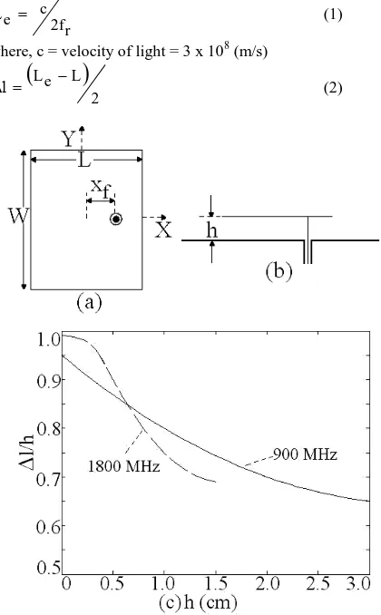
The RMSA suspended in air substrate of thickness ‘h’ is shown in Fig. 1(a, b). To model the fringing field extension length (l), RMSA was designed at different frequencies. At each frequency patch was designed for different substrate thickness. At all the frequencies substrate thickness is taken to be less than 0.10. At 900 MHz, patch length is calculated by using equation (1). Using this value of Le as patch length and with W = 1.2 Le, the antenna was simulated using IE3D software and the peak in its resonance curve is observed. If the peak is not present at 900 MHz, the patch length was changed and the simulation was again carried out. For every iteration, patch width is taken to be 1.2 times the patch length. This procedure is repeated until the peak in the resonance curve is present at around 900 MHz. This simulated value of length (L) is noted and the fringing length (l) is calculated by using equation (2). This procedure is repeated for different values of substrate thickness and for different frequencies and they are plotted in Figs. 1(c) and 2(a). The graphs show l in terms of substrate thickness (h).
r 2f c e
L (1)
where, c = velocity of light = 3 x 10⁸ (m/s)
2 L e L
Δl (2)
Fig. 1 (a) Top and (b) side views of RMSA, and its (c) edge extension plots against substrate thickness
For larger substrate thickness edge extension length due to fringing fields reduces with the frequency. Using the above procedure, an edge extension length for different patch widths at given frequency is calculated and it is plotted in Fig. 2(b, c). For given patch length, with decrease in ‘W’, its resonance
[image:2.595.328.528.112.594.2]frequency increases. Hence for same resonance frequency, patch length is increased, which reduces an edge extension length.
Fig. 2 Edge extension plots against (a) substrate thickness and (b, c) for different widths for RMSA
[image:2.595.60.270.343.682.2]cm and 4.0 cm, respectively. For this dimension, peak in the resonance curve is present at 3452 MHz which is close to the desired frequency with an error of 1.37%. At 5500 MHz, for substrate thickness of h = 0.45 cm (0.080) the patch dimension calculated by using above procedure is, L = 2.1 cm and W = 2.5 cm. This simulated and peak in the resonance curve is present at 5433 MHz which is also close to the desired value with error of 1.2%. Thus the proposed graphs can be used to design the RMSA at any given frequency.
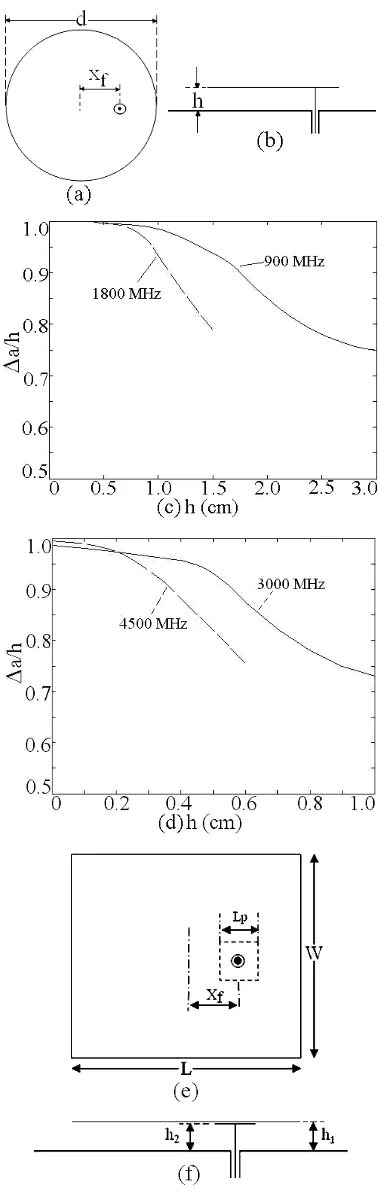
Similar study is carried out for CMSA as shown in Fig. 3(a, b). The resonance frequency of CMSA is calculated by using equation (3). For given substrate thickness, using effective dielectric constant (re) of unity and for fundamental TM11 mode (Kmn = 1.84118), patch radius (ae) is calculated. This is simulated using IE3D software and peak in the resonance curve is observed. If it is not present at desired frequency, by changing the patch radius, simulation is repeated until the peak is obtained at desired frequency. This value of new patch radius (a1) is noted and the extension in patch radius is calculated by using equation (4). This procedure is repeated for different frequencies and substrate thickness and they are plotted in Fig. 3(c, d). Similar to RMSA, an edge extension length reduces with substrate thickness. Using these graphs, CMSA is designed at 1200 MHz. The value of ae obtained using equation (3) is 7.33 cm. Using graphs for 900 MHz, for h = 2.0 cm (0.080), a/h was found to be 0.85, which gives a1 = 5.63 cm by using equation (4). This is simulated and it gives peak in the resonance curve at 1191 MHz which is very close to desired value with an error of 0.75%. Further the CMSA is designed at 3500 MHz. The ae calculated using equation (3) is 2.52 cm. Using graphs for 3000 MHz, for h = 0.7 cm (0.080), a/h was found to be 0.825, which gives a1 = 1.94 cm by using equation (4). This is simulated and the peak in the resonance curve was observed at 3484 MHz which is very close to desired value (error of 0.5%). Thus the proposed graphs can be used to design CMSA on thicker substrates and at desired frequency.
re ε π e 2a c mn K r
f (3)
1 a e a
Δa (4)
3.
PROXIMITY FED MSAs
The proximity fed RMSA is shown in Fig. 3(e, f). The coupling strip is placed below the patch. This configuration is optimized for broader BW at 900 MHz, 1800 MHz and 5500 MHz. At each frequency, substrate thickness for patch (h1) is selected such that it gives h1 = 0.080. Using the above edge extension graphs, RMSA dimensions are selected such that it resonates in TM10 mode. At lower frequencies i.e. below 2500 MHz, the thickness of coupling strip (h2) is selected such that it is placed 0.2 cm below the patch whereas for frequency > 3000 MHz, it is placed 0.1 cm below the patch. At each frequency, optimum BW is obtained by using the parametric study for variations in strip dimensions and its position below the patch. By optimizing these parameters, broader BW at each frequency is obtained. At 900 MHz, simulated BW is 300 MHz. The response is experimentally verified and the measured BW is 289 MHz. At 1800 MHz, the simulated BW is 485 MHz whereas the measured BW is 470 MHz. The simulated BW at 5500 MHz is 1070 MHz whereas the measured BW is 1002 MHz. The design parameter dimensions at above frequencies are given in Table 1.
Fig. 3 (a) Top and (b) side views of CMSA and its (c, d) variation in edge extension length against substrate thickness, (e) top and (f) side views of proximity fed
RMSA
Table 1: Design parameters for proximity fed RMSA
[image:3.595.333.523.77.676.2]Xf 3.5 1.67 0.6
Lp 2.0 1.2 0.4
h1 2.8 1.4 0.5
[image:4.595.363.494.70.187.2]By observing the above parameters, formulation for strip parameters at any given frequencies are, h1 = 0.080, Xf = 0.110, and Lp = 0.0750. Using these parameters the proximity fed RMSAs is designed at 1200 MHz and 3500 MHz. As discussed above, patch dimension at 1200 MHz are, L = 9.7 cm, W = 11.6 cm. The strip of dimension Lp = 1.87 cm is placed at xf = 2.75 cm at substrate thickness of h2 = 1.8 cm. This results in formation of loop inside the VSWR = 2 circle as shown in Fig. 4(a). The simulated BW is 232 MHz whereas the measured BW is 224 MHz. The various design parameters at 3500 MHz, obtained using above formulations are, h1 = 0.7 cm, h2 = 0.6 cm, L = 3.3 cm, W = 4.0 cm, Lp = 0.64 cm, xf = 0.94 cm. It gives simulated BW of 936 MHz whereas the measured BW is 964 MHz as shown in Fig. 4(b).
Fig. 4 Input impedance plots for proximity fed RMSA at (a) 1200 MHz and (b) 3500 MHz, (_____) simulated, (___ ___)
measured
[image:4.595.45.280.72.107.2]Similarly the design guidelines were formulated for proximity fed RMSA with the coupling strip placed inside the patch as shown in Fig. 5. The design formulation for the same is given in Table 2. Using these formulations the RMSA was designed at 2500 MHz and its simulated and measured BW is, 450 MHz (19.7%) and 458 MHz (19.9%), respectively.
[image:4.595.311.548.219.334.2]Fig. 5 Proximity fed RMSA with strip inside the patch
Table 2: Design parameters for proximity fed RMSA with strip inside the patch
Frequency (MHz)
h (cm)
Ls (cm)
Xf (cm)
Lp (cm)
900 3.0 3.4 3.8 2.8
1800 1.5 1.7 1.9 1.4
3000 0.9 1.0 1.1 0.84
5000 0.54 0.6 0.7 0.5
8000 0.34 0.38 0.43 0.32
In terms of
0
0.09λ0 0.102λ0 0.114λ0 0.084λ0
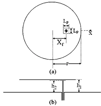
Similarly by using parametric study, proximity fed CMSA as shown in Fig. 6(a, b) is optimized for BW at different frequencies in 800 to 6000 MHz frequency band. The optimized results and various optimized parameters are shown in Table 3 and 4, respectively. Using them design guideline for proximity fed CMSA are formulated as, Xf = 0.1020 and Lp = 0.070.
Fig. 6 (a) Top and (b) side views of proximity fed CMSA
Table 3: Design parameters for proximity fed CMSA
Parameter 900 MHz
2000 MHz
5000 MHz
Xf, (cm) 3.4 1.53 0.65
Lp, (cm) 2.2 1.2 0.5
h1, (cm) 2.7 1.2 0.5
Table 4: Results for proximity fed CMSA
Frequency Simulated BW, MHz, %
Measured BW, MHz, %
900 MHz 261, 28.1 272, 28.9
2000 MHz 443, 21.9 456, 22.2
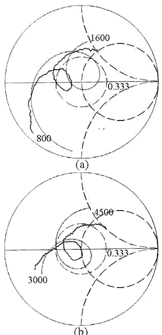
[image:4.595.85.247.278.622.2] [image:4.595.343.508.424.598.2] [image:4.595.314.549.624.766.2]Using these formulations and above edge extension plots, the proximity fed CMSA is designed at 1200 MHz and 3500 MHz. At 1200 MHz, various design parameters are, h1 = 2.0 cm, h2 = 1.8 cm, r = 5.63 cm, xf = 2.55 cm, Lp = 1.75 cm. It gives simulated BW of 302 MHz whereas measured BW is 315 MHz as shown in Fig. 7(a). At 3500 MHz, various design parameters are, h1 = 0.7 cm, h2 = 0.6 cm, r = 1.94 cm, xf = 0.87 cm, Lp = 0.6 cm. It gives simulated BW of 1013 MHz whereas measured BW is 986 MHz as shown in Fig. 7(b). Thus the above parameters can be used to design proximity fed CMSA at any given frequency.
Fig. 7 Input impedance plots for proximity fed CMSA at (a) 1200 MHz and (b) 3500 MHz, (_____) simulated, (___ ___)
measured
The proximity fed ETMSA is shown in Fig. 8(a, b). Using equation (5), patch side length ‘S’ is calculated such that it operates in TM10 mode at desired frequency. Using parametric study, proximity fed ETMSA is optimized for different frequencies in 800 – 8000 MHz frequency band. The results and design parameters for them are tabulated in Table 5 and 6, respectively. From these values the formulations are obtained as, Xf = 0.050, l = 0.0450. The proximity fed ETMSA is designed at 800 MHz using these formulation and the results for the same are shown in Fig. 8(c). The simulated and measured BWs are 206 MHz (25.7%) and 218 MHz (26.7%), respectively.
r ε π e 3S
2 n mn 2 m 2c r
[image:5.595.315.544.76.450.2]f
(5)
Table 5: Results for proximity fed ETMSA
Frequency Simulated BW, MHz, %
Measured BW, MHz, %
1000 MHz 348, 34.8 342, 34.2
2000 MHz 753, 37 742, 36.8
[image:5.595.85.247.190.525.2]3500 MHz 994, 29.1 978, 28.8
Table 6: Design parameters for proximity fed ETMSA
Parameter 1000 MHz 2000 MHz 3500 MHz
Xf, (cm) 2.7 1.2 0.65
l, (cm) 1.5 0.67 0.47
h1, (cm) 2.7 1.35 0.77
Fig. 8 (a, b) Top and side views and (c) input impedance plots for proximity fed ETMSA at 800 MHz, (_____)
simulated, (___ ___) measured
4.
PROXIMITY FED SLOT CUT RMSA
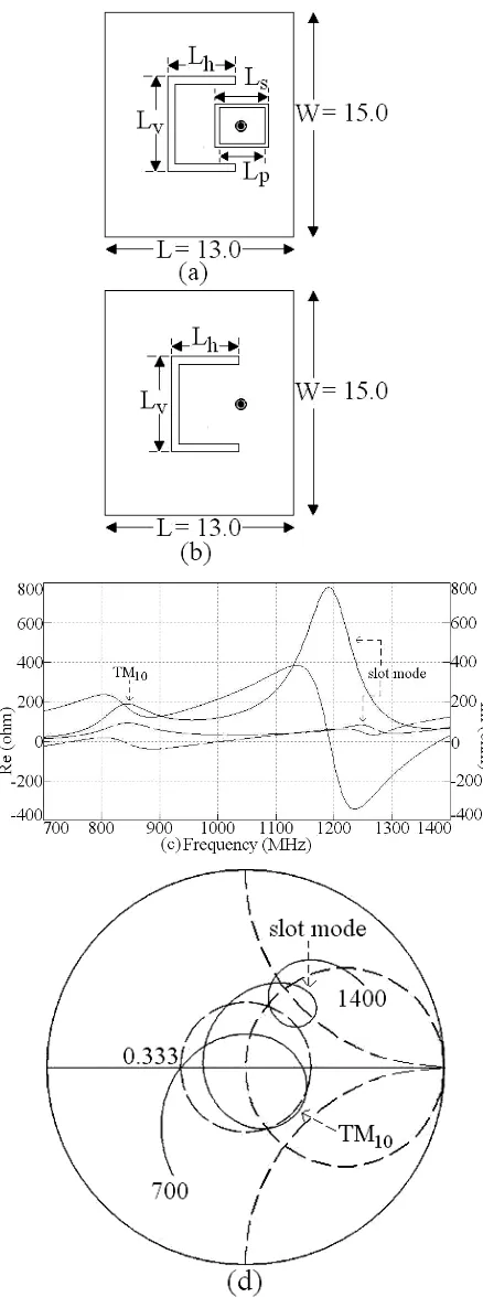
BW as shown in Fig. 10(b). The simulated BW is 478 MHz (45.6%) whereas the measured BW is 470 MHz (45%).The antenna have broadside radiation pattern with gain of more than 7 dBi over the complete BW. The fabricated prototype of the configuration is shown in Fig. 10(c).
Fig. 9 (a) Proximity fed U-slot cut RMSA, (b) coaxially fed RMSA, (c) resonance curve plot for (____) U-slot cut RMSA, (___ ___) proximity fed U-slot cut RMSA and (d) input impedance plot for proximity fed U-slot cut RMSA
Fig. 10 (a) Resonance curve plots for (_____) Lh = 4.7, (___ ___) L
h = 5.1, (b) input impedance plots, (_____) simulated,
[image:6.595.314.542.63.589.2] [image:6.595.55.274.129.722.2]5.
CONCLUSIONS
The formulation for edge extension length for thicker substrates over varying frequencies for RMSA and CMSA is proposed. The graphs for the extension length were developed. Using those, RMSAs and CMSAs were re-designed at different frequencies. It gives closer results with the desired frequency with error less than 2%. The formulation for strip dimension and its position below the patch for given substrate thickness in proximity fed RMSA, CMSA and ETMSA is proposed. Using the proposed formulations the RMSAs and CMSAs were re-designed at different frequencies in 800 – 8000 MHz frequency band. The broadband response with the formation of loop inside the VSWR = 2 circle is obtained. Further by using the proposed formulations for proximity fed RMSA, a detail design procedure for proximity fed U-slot cut RMSA is presented. It also shows the formation of loop inside the VSWR = 2 circle with a broader BW of more than 450 MHz. Thus the proposed formulations for edge extension length and strip parameters can be used to design RMSA, CMSA or ETMSA at any given frequency and substrate thickness.
6.
REFERENCES
[1] Kumar, G., and Ray, K. P. 2003, Broadband Microstrip Antennas, First Edition, USA, Artech House [2] Garg, R., Bhartia, P., Bahl, I., and Ittipiboon, A.,
Microstrip Antenna Design Handbook, 2001, Artech House, USA.
[3] Cock, R. T., and Christodoulou, C. G. 1987. Design of a two layer capacitively coupled, microstrip patch antenna element for broadband applications, IEEE Antennas Propag. Soc. Int. Symp. Dig., vol. 2, 936-939. [4] Huynh, T., and Lee, K. F. 1995. Layer
Single-Patch Wideband Microstrip Antenna, Electronics Letters, vol. 31, no. 16, (August 1995), 1310-1312.
[5] Lee, K. F., Yang, S. L. S., Kishk, A. A., and Luk, K. M. 2010. The Versatile U-slot Patch, IEEE Antennas & Propagation Magazine, vol. 52, no. 1, (February 2010), 71 – 88.
[6] Guo, Y. X., Luk, K. M., Lee, K. F., and Chow, Y. L. 1998. Double U-slot Rectangular Patch Antenna, Electronics Letters, vol. 34, 1805 – 1806
[7] Sharma, S. K., and Shafai, L. 2009. Performance of a Novel -Shaped Microstrip Patch Antenna with Wide Bandwidth, IEEE Antennas & Wireless Propagation Letters, vol. 8, 468 –471.
[8] Wong, K. L. 2002. Compact and Broadband Microstrip Antennas, John Wiley & sons, Inc., New York, USA
[9] Deshmukh, Amit A., Joshi, Apurva A., and Tirodkar, T., Broadband slot cut gap-coupled proximity fed E-shaped Microstrip Antenna, International Journal of Computer Application, vol. 68, no. 17, April 2013, 15 – 18
[10] IE3D 12.1, 2004. Zeland Software, Freemont, USA [11] Balanis, C. A., Antenn Theory: analysis and design,