Speeding-up Phase-Locked Loops based on Adaptive
Loop Bandwidth
Dina M. El-Laithy
Communications Engineering Department
Modern Academy of Engineering and Technology
Cairo, Egypt
Abdelhalim Zekry
Communications Engineering Department
Faculty of Engineering Ain shams University
Cairo, Egypt
Mohamed Abouelatta
Communications Engineering Department
Faculty of Engineering Ain shams University
Cairo, Egypt
ABSTRACT
This paper describes three techniques for controlling the loop filter of the PLL for high operating speed. The proposed fast-locking PLL reduces the pull-in time and enhances the switching speed, while maintaining better noise bandwidth. Extended loop bandwidth enhancement is achieved by the adaptive control on the loop filter resistances. This work differs from previously published results in that it presents a comprehensive study for modeling, circuit simulation and practical circuit implementation of a 2nd order PLL with loop filter control for speeding-up the PLL. The overall improvement in performance of the proposed PLL is evaluated and compared with the conventional PLL. An industrial CMOS IC is used to implement the PLL.
General Terms
Electronic design, Communications, Simulation, Hardware.
Keywords
Phase locked loop, speeding-up, adaptive bandwidth, natural frequency, settling time
1.
INTRODUCTION
Phase-locked loops (PLLs) have been used in many applications ranging from communications, radar to automobiles. In the recent past, digital phase-locked loops have been widely used in high-performance microprocessors and high-speed digital communication systems as clock generators [1],[2]. As the speed of these systems increasing, the PLLs with higher operating frequency and lower jitter are in demand. So in nearly all the PLL applications, it is required to generate low noise while achieve fast settling time. The settling time is largely determined by the loop bandwidth. In some applications, the loop bandwidth should be made as narrow as possible to minimize output phase jitter due to external noise, resulting in an elongated settling time. One of the solutions to this problem is the adaptive PLL using a wide bandwidth in the out-of-lock state and switching to a narrow bandwidth as the loop settles. With the adaptive PLL, one could speed up the settling process while ensuring sufficient reference feed-through attenuation for low output noise. For many adaptive PLL’s in literature [3-5], the loop bandwidth enhancement is achieved by increasing the charge pump current and/or increasing the loop gain [6]-[8],[11]-[14]. However, the loop bandwidth is still constrained by the reference frequency for loop stability considerations. Another method of loop bandwidth enhancement is achieved by using a nonlinear loop filter instead of a conventional loop filter [9]. But it is difficult to implement. To expand the loop bandwidth even further, a new adaptation scheme is proposed that not only increases the bandwidth, but also gives good noise performance. This paper describes three improved acquisition
techniques designs and it is organized as follows: Section 2 presents the detailed circuits of the proposed PLL for speeding-up acquisition. The simulation results are discussed in Section 3. Section 4 illustrates the experimental results. The conclusions are given in Section 5.
2.
OPERATING PRINCIPLE OF THE
PROPOSED PLL FOR SPEEDING-UP
ACQUISITION
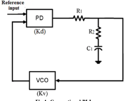
A conventional PLL is shown in Fig. 1. It is composed of an XOR phase detector, a loop filter and a voltage-controlled oscillator. The first-order loop filter is composed of the resistors R1 and R2 and the capacitor C1. The damping factor and natural
frequency are approximately expressed as [10]
= and ζ=
(1)
Where Kd is the phase detector gain and Ko is the gain of the
VCO. The bandwidth of a PLL is often specified by the 3-dB corner frequency ω3db and it is expressed as [10]:
= (2)
For a damping factor ζ = 0.7, ω3db becomes ω3db = 2.05 ωn,
which is about twice the natural frequency. From Eq. (1) and Eq. (2) to speed-up PLL, the loop bandwidth enhancement is achieved by increasing the natural frequency ωn by reducing the
[image:1.595.318.528.570.738.2]time constants of the loop filter.
This can be accomplished by applying different methods to change the loop filter resistances R1 or R2 in the out-of-lock state. The change in the loop filter resistance depends on the difference between the input and the output frequencies; as this difference decreases, the resistance changes to obtain smooth transition to lock. A frequency difference sensing circuit is used to represent the difference between the input and output frequencies by a certain voltage to control the loop filter resistance.
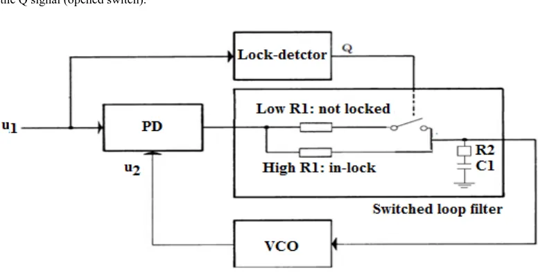
The first proposed design is shown in Fig. 2. It presents the proposed PLL with a lock detector. In this configuration the loop filter bandwidth can be switched by a binary signal. The control signal for the switched filter is derived from the lock-in detector. In the unlock state of the PLL, the output signal Q of the lock-in detector is high. In this state, the switch is closed given a low resistance loop filter which widens the loop bandwidth as explained before.
The noise bandwidth is then too large. The filter bandwidth has to be reduced instantaneously to a value where the noise bandwidth is small enough to provide stable operation. This is done by switching the loop filter to its low bandwidth position by means of the Q signal (opened switch).
In the second proposed design, a grounded capacitor C together with two switches replaces a resistor R1 as shown in Fig. 3. The two switches are driven by a non overlapping two phase clock. The clock frequency fs is much higher than the frequency of the input. Thus during clock phase φ1, when C is connected across the input voltage Vin, the variations in the input signal are negligible small. It follows that during φ1 capacitor C charges up to the voltage Vin. Then, during clock phase φ2, capacitor C is connected to the output, as indicated in Fig. 3 Capacitor C is thus forced to discharge, and its previous charge is transferred to the output.
From the description above, during each clock period T an amount of charge is extracted from the input and supplied to the output. If T is sufficiently short, this process as almost continuous and define an equivalent resistance Req between
input node and output node.
[image:2.595.100.488.307.504.2]= (3)
Fig 4: A block diagram of the proposed PLL using a switched-capacitor resistor technique to control the filter
bandwidth
In this technique the proposed PLL is designed to achieve fast locking by replacing the filter resistance R1 by a switched-capacitor resistor and adding a frequency difference sensing circuit to produce a clock signal representing the difference between input frequency and output frequency. The clock signal is used to control the two switches S1 and S2 of the switched capacitor resistor as shown in the Fig. 4.
In the unlock state of the PLL, the frequency difference between the input frequency and the output frequency is large. According to Eq. (3) the equivalent resistance is small which widens the loop bandwidth and reduce the acquisition time.
As frequency difference between input frequency and output frequency decreases, the equivalent resistance to the switched-capacitor increases and so the loop bandwidth decreases until it reaches its conventional value at locking. Hence, we obtain smooth transition to lock.
[image:3.595.313.540.74.231.2]The third proposed PLL is designed to achieve fast locking by replacing the filter resistance R2 by a JFET transistor working as a voltage controlled resistance and adding a frequency difference sensing circuit to produce a voltage proportional to the frequency difference between input and output. This voltage is applied to the JFET gate to control the resistance value between the drain and source terminal.
Fig 5: A block diagram of the proposed PLL using VCR
A frequency to voltage converter circuit is used to give a control voltage representing the frequency difference between input and output frequencies as shown in Fig. 5.
The output voltage from the frequency difference sensing circuit is inversely proportional to the frequency difference. In the unlock state of the PLL, the output voltage has a low negative value, hence the equivalent resistance between drain and source terminal of the VCR is low which widens the loop bandwidth as explained before.
As the frequency difference decreases the output voltage increases negatively, hence the equivalent resistance will increase and so the loop bandwidth decreases until reaching its conventional value at locking. Hence, we obtain smooth transition to lock.
3.
SIMULATION RESULTS
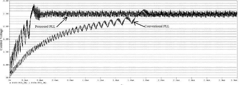
For the first proposed design Fig. 6 and Fig. 7 show the SPICE circuit used for both the conventional PLL and the proposed PLL, respectively. Fig. 8 shows the simulated transient responses for the conventional PLL and the proposed one. Performance summaries are listed in Table 1. From Fig. 8, the locked time is 2.1 ms for the conventional PLL. While it amounts only to 1.4 ms for the proposed PLL.
Fig 6: Schematic of the conventional PLL Fig 7: Schematic of the first proposed PLL (S =analog
[image:3.595.315.546.549.701.2] [image:3.595.43.276.550.712.2]Fig 8: Simulated transient of the conventional PLL and the 1st proposed PLL
[image:4.595.60.520.291.510.2]For the second proposed design, Fig. 9 shows the SPICE circuit used for the proposed PLL. Fig. 10 shows simulated transient responses for the conventional PLL and the proposed PLL. Performance summaries of this work are also listed in Table 1. The lock time is 2.1 ms in the conventional PLL. It amounts to 0.5 ms for the proposed PLL.
[image:4.595.59.305.339.504.2]Fig 9: Schematic of the second proposed PLL (S1 and S2 =analog switch (4016))
Table 1 Performance summary of the proposed PLL
Supply voltage 5V
Reference input 100 KHz VCO center frequency 85 KHz VCO's frequency range 17-150 KHz with
Kv = 206 KHz/V R1 in loop filter 10 KΩ (conventional)
5 KΩ (proposed) R2 in loop filter 3 KΩ C1 in loop filter 10 nF Simulated settling time 2.1 ms (conventional)
1.4 ms (1st proposed) 0.5 ms (2nd proposed) 0.5 ms (3rd proposed) Measured settling time 2.1 ms (conventional) 1.2 ms (1st proposed) 0.5 ms (2nd proposed) 0.3 ms (3rd proposed)
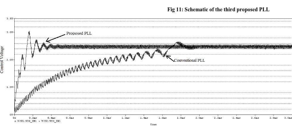
[image:4.595.92.510.562.711.2]For the third proposed design Fig. 11 shows the SPICE circuit used for the proposed PLL. Fig. 12 shows simulated transient responses for the proposed PLL. Performance summaries of this work are also listed in Table 1. The lock time is 2.1 ms in the conventional PLL. In Fig. 12, the lock time for the proposed PLL is reduced to be 0.5 ms.
[image:5.595.58.548.257.471.2]Fig 11: Schematic of the third proposed PLL
Fig 12: Simulated transient of the conventional PLL and the 3rd proposed PLL
4.
Experimental results
The practical implementation for the conventional and proposed PLL are carried out to verify the results obtained by computer simulations. The circuits shown in Fig. 6, Fig. 7, Fig. 9 and Fig. 11 have been completely built and tested in the laboratory. The circuits have been tested with a frequency step input and the time response of the PLL was measured. Results of these experimental work are also listed in Table 1.
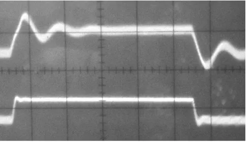
Fig. 13, Fig. 14 and Fig. 15 show the measured transient responses for the conventional PLL and the 1st, 2nd, 3rd proposed ones to demonstrate the speeding-up, respectively. The measured locked time is 2.1 ms in the conventional PLL and the proposed one is 1.4 ms, 0.5 ms and 0.5 ms, respectively. The measurement results match with high-degree the simulated results.
[image:5.595.310.546.519.684.2]Fig 14: Measured transients of the conventional PLL with the 2nd proposed PLL
Fig 15: Measured transients of the conventional PLL with the 3rd proposed PLL
5.
CONCLUSION
In this paper, a complete study to design high speed PLL is achieved. This paper demonstrates three techniques for fast-acquisition PLL. To speed-up PLL, the loop bandwidth enhancement is achieved by increasing the natural frequency ωn by reducing the time constants of the loop filter. Adding a frequency difference circuit to represents the difference between input frequency and output frequency to control the loop filter time constants. Simulation and measurement results show that, a lock time reduction up to 75% was achieved compared with the conventional PLL. The measurement results demonstrate the proposed circuits.
6.
ACKNOWLEDGEMENT
The authors would like to thank the Department of Electronics & Communication Engineering, Ain Shams University, for providing its laboratory and library facilities.
7. REFERENCES
[1] Mozhgan Mansuri, Dean Liu, and Chih-Kong Ken Yang et al., “Fast frequency acquisition phase-frequency detectors for Gsamples/s phase-locked loops,” IEEE Journal of Solid-State Circuits, Vol. 37, No. 10, Oct. 2002, pp. 1331– 1334.
[2] W. C. Lindsey and C. M. Chie, Phase-Locked Loops. New York. IEEE Press, 1986.
[3] C.S. Vaucher. "An adaptive PLL tuning system architecture combining high spectral purity and fast settling time," IEEE Journal of Solid-State Circuits, Vol. 35, pp. 490-502, 2002.
[4] J. Lee and B. Kim, "A low-noise fast-lock phase-locked loop with adaptive bandwidth control," IEEE Journal of Solid-State Circuits, Vol. 35, pp. 1137-1145, 2002.
[5] S. Sidiropoulos, D. Liu, J. Kim, G. Wei and M. Horowitz, "Adaptive bandwidth DPLLs and PLLs using regulated supply CMOS buffers," Symposium on VLSI Circuits Digest of Technical Papers, pp. 124-127, 2002.
[6] B. Kim, “High speed clock recovery in VLSI using hybrid analog/digital techniques,” Ph.D. dissertation, Univ. California, Berkeley, June 1990.
[7] B. S. Glance, “New phase-lock loop circuit providing very fast acquisition time,” IEEE Trans. Microwave Theory Technol., vol. MTT-23, pp. 747–754, Sept. 1985.
[8] Crowley, “Phase locked loop with variable gain and bandwidth,” U.S. Patent 4,156,855, May 29, 1979.
[9] D. Williamson, “Improved phase-locked loop performance via nonlinear loop filters,” IEEE Trans. Commun., vol. COM-27, pp. 542-556, Mar. 1979.
[10]R. E. Best, Phase-Locked Loops: Theory, Design and Applications. New York, NY: fifth edition, McGraw-Hill, 2003.
[11]M. F. Wagdy and S. Vaishnava, "A Fast-Locking Digital Phase-Locked Loop," Proceedings of the 3rd International Conference on Information Technology: New Generations (ITNG-2006), Las Vegas, Nevada, pp.742-746, April 10-12, 2006.
[12]J. J. McDonald, and R. B. Hulfachor, “Circuitry to Reduce PLL LockAcquisition Time,” U. S. Patent # 6,940,356, September 6, 2005.
[13]Assaf Ben-Bassat and Haifa “PLL Lock Time Reduction,” U. S. Patent #7,595,698, Sep. 29, 2009.
[14]James A. Crawford, "Advanced Phase-Lock Techniques", Artech House, Boston, 2008.
[image:6.595.56.303.270.411.2]