OEM MICRONOTES
mamaala
Enclosed is the new set of MicroNotes. twenty-one new documents relating component products from Digital.
This set to some of
consists of the latest
The original set of 111 MicroNotes has been superseded by this new edition. The titles in the original set can be found in Appendix A of the enclosed document. The original MicroNotes (if- you do not have them) can still be obtained by wri ting to the OEM Technical Support Group at:
OEM Micros Technical Support Group Digital Equipment Corporation
2 Iron Way MR03-3/G20 Marlboro, MA 01752 Attn: Cindy Dorval
Be sure to ask for the original MicroNotes.
If there is someone you know that would like to be added to the MicroNote Distribution List have them fill out the enclosed MicroNote Reservation Form and return it to the address listed above.
The group would appreciate any feedback or suggestions on future MicroNotes these comments can also directed to the above address.
Sincerely,
Digital Equipment Corporation Two Iron Way . Box 1003
Marlboro, Massachusetts 01752-9103 617.467.5111
Your name is on our mailing list. Enclosed is an updated set of MicroNotes which consists of the twenty-one previously published documents plus twenty NEW MicroNotes. The information contained in this set relates to some of the latest component and small system products from Digital.
If someone would like to be added to the MicroNote Distribution List, have them fill out the enclosed MicroNote Reservation Form and return it to the address listed below; attention Cindy Dorval. This form can also be used to make address corrections, noting the date your location changed.
The group would appreciate any feedback or suggestions for future MicroNotes. These comments can also be directed to the address below.
Thank you for your continuing interest.
OEM Technical Support Group Digital Equipment Corporation 2 Iron Way (MR03-3/G20)
MicroNote Reservation Form
_ _ _ _ _ _ _ ~---_ _ _ _ _ _ I _ _ _ _ _ _ - - - _ _ _ _ _ _ _ _ _
Please fill out this form and return it to:
OEM Micros Technical Support Group Digital Equipment Corporation
2 Iron Way MR03-3/G20 Marlboro, MA 0172
Attn: Cindy Dorval
This will add you to the MicroNote Di~tribution List. MicroNotes are short technical articles written about Digital's component level products. Product highlights, technical descriptions, technical hints-and-kinks not found in the regular documentation, and recent product changes and announcements are discussed in the MicroNotes.
Name: Company: Title: Address: City:
State: Zip:
Questionnaire
1. I am:
o an OEM
o a Distributor o an End-User o Other
2. The Industry I Service is (e.g. Instrumentation, Education):
Medical,
3. The Application(s) within that Industry is/are machine control, IC testers, general purpose computing):
4. I'd like future MicroNotes to Discuss:
Control,
TABLE OF CONTENTS
uNOTE NO. TITLE
001 002 003 004 005 006 007 008 009 010 011 012 013 014 015 016 017 018 019
MUL, DIV, & ASH Instruction for the FALCON and the FALCON-PLUS
Block Mode DMA
Compatible Bootstrap for the LSI-11/73 LSI-11/73 Upgrade Paths
Q22 Compatible Options
Differences Between the LSI-ll/73 and LSI-11/23
User Defined Memory Maps for the FALCON and the FALCON-PLUS
Memory Management and the LSI-l1/73 Cache Concepts and the LSI-l1/73 MicroVAX I/O Programming
LSI-11/73 Advanced Memory Management OMA on the Q-bus
Run-time System Performance Evaluation Using MicroPower/Pascal V 1.5
Using Fortran Routines In A VAXELN/pascal Environment Q-bus Hardware Bootstrap
KXTI1-CA Software Development Tools LSI-11/23 ECO History
Programming the KXTII-CA DM.~ Controller Disabling RAM on the MXV11-iBF
DATE 13-Apr-82 01-Jun-83 28-Nov-83 28-Nov-83 23-Apr-84 23-Apr-84 01-May-84 22-Jun-84 02-Jul-84 27-Jul-84 04-0ct-84 09-0ct-84 09-0ct-84 16-0ct-84 16-0ct-84 16-0ct-84 19-Nov-84 28-Dec-84 10-Jan-85
PAGE NO.
uNOTE NO. TITLE 020 021 022 023 024 025 026 027 028 029 030 031 032 033 034 035 036 037 038 039 040 041
Differences between the Mxv11-A and MXV11-B
Floating Point Consideration on MicroVAX I
Differences Between the MicroVAX I and MicroVAX II CPUs
MicroVAX I to MicroVAX II Upgrade Issues MicroVAX Instruction Set Differences FPJ11-AA Compatibility with the
LSI-11/73 (KDJ11-A)
The MicroVAX Multicomputing Capability Using Messages with VAXELN
MSV11-Q/M/J Memory Comparisons Q-bus Expansion Concepts
The Private Memory Interconnect between the KDJ11-B and the MSV11-J
MSV11-QA Revision Differences KXT11-C Parallel I/O Programming
System Configuration of DL-type Devices Programming the KXT11-C Multiprotocal SLU Backplane Expansion/Termination
MicroVMS Revealed In Search of NanoVMS DECnet Downline Loading
Differences between KDJ11-A and KDJ11-B FPJ11 Theory of Operation
Device Ordering Chart for Q-bus Systems
DATE 10-Jan-85 10-Jan-85 28-Apr-85 28-Apr-85 28-Apr-85 28-Jun-85 28-Jun-85 28-Jun-85 28-Jun-85 28-Jun-85 28-Jun-85 28-Jun-85 28-Jun-85 28-Jun-85 19-Jul-85 19-Jul-85 19-Jul-85 19-Jul-85 26-Jul-85 08-Aug-85 17-Sep-85 17-Sep-85
PAGE NO.
APPENDIX A
ORIGINAL MICRONOTES - TABLE OF CONTENTS APPENDIX B
SUBJECT INDEX
A1
· I
uNOTE # 001Title: MUL,DIV and ASH Instruction for the FALCON
Date: 13-APR-82
and the FALCON-PLUS
Originator: Charlie Giorgetti
Page 1 of
4uNOTE # 001 Page 2 of 4
The following macro and subroutine can be used to perform the MUL instruction in software:
• MACRO MOV MOV JSR MOV MOV .ENDM $MUL: : MOV
MOV MOV MOV CLR 10$: ROR ROR BCC ADD CLC 20$: DEC BNE TST MOV MOV MOV MOV RTS
SMUL A,B,HI,LO A,-(SP) B,-(SP) PC,$MUL (SP)+,HI (SP)+,LO RO,-(SP) R1,-(SP) 10(SP),R1 #21,-(SP) RO RO Rl 20$ 10(SP),RO (SP) 10$ (SP)+ R1,10(SP) RO,6(SP) (SP)+,Rl (SP)+,RO PC
Push a multiplier onto the stack Push the other multiplier as well Call the MUL subroutine
Get the most significant part of the result
Get the least significant part of the result
Save some work registers
Obtain the value of A from the stack Initialize the shift counter
; Initialize the high 16-bit accumulator Perform multiplication
Bump the shift counter Not done ?
Romove the counter from the stack
Save the low 16-bit value on the stack Save the high 16-bit value on the stack Restore the work registers
uNOTE # 001 page 3 of 4 The following macro and subroutine can be used to perform the DIV instruction in software:
.MACRO SDIV DIVSOR,DIVHI,DIVLO,REM,QUO MOV MOV MOV JSR MOV MOV .ENDM $DIV:: MOV
MOV MOV MOV MOV MOV MOV CLR MOV 1$: ASL ROL ROL CMP BLO SUB I~C 2$: DEC
BNE TST MOV MOV MOV MOV MOV MOV MOV RTS DIVSOR,-(SP); DIVHI ,-( SP) i
DIVLO ;-( SP) i
PC,$DIV ; (SP)+,REM (SP)+,QUO
Push the divisor onto the stack
Push the upper 16-bits of the dividend Push the lower 16-bits of the dividend Call the DIV subroutine
Get the remainder Get the quotient
.RS ,-(SP) R4,-(SP) R3,-(SP) RO,-(SP) 14.(SP),R3 12.(SP),R4 10. (SP) , RS RO #32.,-(SP) RS R4 RO RO,R3 2$ R3,RO RS (SP) 1$ (SP)+ RO,12.(SP) RS,14.(SP) (SP)+,RO (SP)+,R3 (SP)+,R4 (SP)+,RS (SP)+,(SP) PC
; Get some work registers
Get the divisor from the stack
i Get the high 16-bits of the dividend as well as low 16-bits
i Clear an accumulator ; Shi :Et counte r
Perform the division
Not done ?
; Remove the counter from the stack Store the remainder on the stack ; store the quotient as well
Restore the work registers
uNOTE .# 001 Page 4 of 4
The following macro and subroutine can be used to perform the ASH instruction in software:
. MACRO MOV MOV JSR MOV .ENDM $SASH: : MOV
MOV MOV MOV BIC BEQ CMP
~ BGT
5$: ASL DEC BNE BR 10$: NEG
BIC 11$: ASR DEC BNE 20$: MOV MOV MOV MOV RTS
SASH COUNT,VAL COUNT,-(SP) VAL,-(SP) PC,$ASH (SP)+,VAL RO,-(SP) R1,-(SP) 6(SP),RO 8.(SP),R1 #"C<77>,R1 20$ R1,#31. 10$ RO R1 5$ 20$ R1 #"C<77>,R1 RO R1 11$ RO,8.(SP) (SP)+,R1 (SP)+,RO (SP)+,(SP) PC
; Push the shift count
Push what is to be shifted Call the ASH subroutine
Get the results of the shift
Get a couple of work registers RO - value to be shifted
R1 - direction and shift count Get out if no shifting
; What direction is the shift
go to the corection direction shift
Store the shifted result on the stack Restore the work registers
uNOTE # 002
Title: Block Mode DMA Date: 01-JUN-83
Originator: Scott Tincher and Mike Collins Page 1 of 20
What is Block Mode DMA?
Block Mode DMA is a method of data transfer which increases throughput due to the reduced handshaking necessary over the Q-bus. In order to implement Block Mode DMA both the master and slave devices must understand the block Mode protocol. If either device does not have Block Mode capability the transfers proceed via standard DATI or DATO cycles.
Conventional Direct Memory Access on the Q-bus
Under conventional DMA operations, after a DMA device has become bus master, i t begins the data transfers. This is accomplished by gating an address onto the bus followed by the data being transferred to or from the memory device. If more than one transfer is performed by the temporary bus master, the address portiort of the cycle must be repeated for each data transfer.
Block Mode Direct Memory Access on the Q-bus
uNOTE
:1
002Page 2 of 20
There are two types of block Mode transfer, DATBI (input) and DATBO (output). An overview of what occurs during each type of block Mode transfer is outlined in figures 1 (DATBI, Block Mode input.) and 2 (DATBO, block mode output).
In the following discussion the signal prefix bus driver input and the signal prefix
receiver output.
DATBI Bus Cycle
T(Transmit) indicates a R(Receive) indicates a bus
Before a DATBI block mode transfer can occur the DMA bus master device must request control of the bus. This occurs under conventional Q-bus protocol ..
o REQUEST BUS
The bus master device requests control of the bus by asserting TDMR ..
o GRANT BUS CONTROL
The bus arbitration logic in the CPU asserts the DMA grant signal TDMGO 0 nsec minimum after TDMR is received and 0 nsec minimum after RSACK negates (if a DMA device was previous bus master) .
o ACKNOWLEDGE BUS MASTERSHIP
The DMA bus master device asserts TSACK 0 nsec minimum after receivin~ ,RDMGI, 0 nsec minimum after the negation of RSYNC and
o
nsec mlnlmum after the negation of RRPLY. The DMA bus master device negates TDMR 0 nsec minimum after the assertion of TSACK.o TERMINATE GRANT SEQUENCE
o EXECUTE A BLOCK MODE DATBI T~ANSFER
o ADDRESS DEVICE MEMORY
uNOTE # 002 Page 3 of 20
a) The address is asserted by the bus master on TADDR<21:00> along with the negation of TWTBT.
b) The bus master asserts TSYNC 150 nsec minimum after gating the address onto the bus.
o DECODE ADDRESS
The appropriate memory device recognizes that i t must respond to the address on the bus.
o REQUEST DATA
a) The address is removed by the bus master from TADDR<21:00> 100 nsec minim,um after the assertion of TSYNC. b) The bus master asserts the first TDIN 100 nsec minimum after asserting TSYNC.
c) The bus master asserts TBS7 50 nsec maximum after asserting TDIN for the first time. TBS7 remains asserted until 50 nsec maximum after the assertion of TDIN for the last time. In each case, TBS7 can be asserted or negated as soon as the conditions for asserting TDIN are met.
The assertion of TBS7 indicates the bus master is requesting another read cycle after the current read cycle.
o SEND DATA
a) The bus slave asserts TRPLY 0 nsec m~n~mum (8000 nsec maximum to avoid a bus timeout) after receiving RDIN.
b) The bus slave asserts TREF concurrent with TRPLY if, and only if, i t is a block mode device which can support another RDIN after the current RDIN.
NOTE
Block mode transfers must not cross boundaries
uNOTE # 002 Page 4 of 20
c) The bus slave gates TDATA<15:00> onto the bus 0 nsec minimum after receiving RDIN and 125 nsec maximum after the assertion of TRPLY.
o TERMINATE INPUT TRANSFER
a) The bus master receives stable RDATA<15:00> from 200 nsec maximum after recelvlng RRPLY until 20 nsec minimum after the negation of RDIN. (The 20 nsec minimum represents total minimum receiver delays for RDIN at the slave and RDATA<15:00> at the master.)
b) The bus master negates TDIN 200 nsec minimum after receiving RRPLY.
o OPERATION COMPLETED
a) The bus slave negates TRPLY 0 nsec minimum after receiving the negation of RDIN.
b) If RBS7 and TREF are both asserted when TRPLY negates, the bus slave prepares for another DIN cycle. RBS7 is stable from 125 nsec after RDIN is received until 150 nsec after TRPLY negates.
c) If TBS7 and RREF were both asserted when TDIN neg~t~d, the bus master asserts TDIN 150 nsec minimum after recelvlng the negation of RRPLY and continues with timing relationship 'SEND DATA' above. RREF is stable from 75 nsec after RRPLY asserts until 20 nsee minimum after TDIN negates. (The 0 nsee mlnlmum represents total minimum receiver delays for RDIN at the slave and RREF at the master.)
NOTE
o TERMINATE BUS CYCLE
uNOTE # 002 Page 5 of 20
a) Ie RBS? and TREF were not both asserted when TRPLY negated, the bus slave removes TDATA<15:00> from the bus
0
nsec minimum and 100 nsec maximum after negating TRPLY.
b) If TBS? and RREF were not both asserted when TDIN negated the bus master negates TSYNC 250 nsec minimum after receiving the last assertion of RRPLY and 0 nsec minimum after the negation of that RRPLY.
o RELEASE THE BUS
a) The DMA bus master negates TSACK
0
nsec after negation of the last RRPLY.b) The DMA bus master negates TSYNC 300 nsec maximum after i t negates TSACK.
c) The DMA bus master must remove RDATA<15:00>, TBS?, and TWTBT from the bus 100 nsec maximum after clearing TSYNC.
uNOTE # 002 Page 6 of 20
PROCESSOR
Figure 1 - DATSI CYCLE
I/O DEVICE
5
Assert TDMR Request Bus Grant Bus Control <. Near end of the current bus cycle (RRPLY is negated) assert TDMGO and inhibit new processor generated TSYNC for the duration
MEMORY
of the DMA
ope~:
Acknowledge Bus MastershipI
V
· Receive RDMGO
· Wait for negation of RSYNC and RRPLY · Assert TSACK
Negate TDMR
Terminate Grant Sequence
DMA
(DATSI) Data Transfer
Address Device Memory
· Assert address on TADDR<21:00> · Assert TSYNC
· Negate TWTBT ~
~>
Decode Address. Store "Device
[image:17.612.108.558.90.674.2]PROCESSOR
uNOTE # 002 Page 7 of 20
Figure 1 - DATSI CYCLE (continued)
I/O DEVICE MEMORY
r---> Request Data
· Remove address from TADDR<21:00> · Assert TDIN
· Assert TBS7 (request for an additional DIN cycle after the curre!nt one
L _____
> Send Data· Data on TDATA<15:00> · Assert TRPLY
· Assert TREF (to indicates block mode capability) Terminate' Input <---'1
Transfer
· Accept data and respond by nega,ting TDIN
L ______
> Operation Completed . Negate TRPLY1
yes are
~---~RBS7 & TREF Asserted
?
I
no,---'
[image:18.617.187.537.82.595.2]uNOTE # 002
Page 8 of 20
Figure 1 - DATBl CYCLE (continued)
PROCESSOR
I
V
I/O DEVICE
Terminate Bus Cycle and Release the Bus
· Negate TSACK · Negate TSYNC
· Remove TDAL, TBS?, and, TWTBT from the Bus
Resume Processor Operation
. Enable processor generated TSYNC or issue another grant if RDMR is asserted
[image:19.615.141.557.57.719.2]T
R DMG
T SAO:
...
_--,-""""
T/R D.AL __________ - J
R/T
100 ns
T O:N
~ RE:
---~---~~
I
'
~\
:15 \
ns ::tax
uNOTE #002 Page 9 of 20
,.,. 35_7 _ _
"---'r
~ ~-.~\ \\\)\\~
10 \ \ \ \ " \ \ \ \ \ \ \
\\\\\S\\S\\\\\\
~iminq at slave device. - • bus driver input
uNOTE #002 Page 10 of 20
R ADDR
uNOTE #002
page 11 of 20
'!' DATA
ns :nax ____ 1
~----~--~--~---~--~
R SYNC
R D!~
t
!
R 857
/
~~:n~ng a~ slave dev~ce.
7 • bus driver in~ut
~ • Sus rece~ver OU~?~:
\
/
\
'L
\
uNOTE #002 page 12 of 20
DATBO Bus Cycle
uNOTE
#002
Page 13 of 20
DATBO Bus cycles Before a block mode transfer can occur
the
DMA
bus
master device must
request control
of the
bus.
This occurs under
conventional Q-bus protocol.
o REQUEST BUS The bus master device requests control of the bus by
asserting TDMR.
o GRANT BUS CONTROL The bus arbItration logic in the CPU
asserts
the
DMAgrant signal TDMGO 0 nsec minimum after RDMR is received
and 0 nsec minimum after TSACK negates
(if a
DMA
device was
previous bus master).
o ACKNOWLEDGE BUS MASTERSHIP The DMA
bus master device
asserts
TSACK 0 nsec minimum after receiving RDMSI, 0 nsec minimum after
the negation of RSYNC and 0 nsec minimum after the
negation of
RRPLY.,
The
DMA
bus master device negates TDMR 0 nsec minimum
after the assertion of TSACK.
o TERMINATE GRANT SEQUENCE The bus arbitration logic
in the
CPU
negates TDMGO
0
nsec minimum after receiving RSACK.
The bus
arbitration logic will also ne9ate TDMGO if RDMR negates
or
if
RSACK fails to assert within 10 usec ('no SACK timeout').
o EXECUTE A BLOCK MODE DATBO TRANSFER
o ADDRESS DEVICE MEMORY
a) The address is asserted by the bus master on TADDR<21:00>
along wi th the assertion of T'WTBT.
b) The bus master
asserts TSYNC
150
nsec minimum
after
gating the address onto the bus.
o DECODE ADDRESS The appropriate memory device recognizes that
it must respond to the address on the bus.
o SEND DATA
a) The bus master gates TDATA<15:00> along with TWTBT
100
nsee minimum
after the
assertion of TSYNC.
TWTBT
is
negated.
b) The bus master asserts the first TDOUT 100
nsec minimum
after gating TDATA<15,: 00>.
NOTE
uNOTE # 002 Page 14 of 20
o RECEIVE DATA
a) The bus slave receives stable data on RDATA<15:00> from 25 nsec minimum before receiving RDOUT until 25 nsec minimum after receiving t~e negation of RDOUT.
b) The bus slave asserts TRPLY 0 nsec minimum after receiving RDOUT.
c) The bus slave asserts TREF concurrent with TRPLY if, and only if, it is a block mode device which can support another RDOUT after the current RDOUT.
NOTE Blockmode transfers must boundaries
not cross 16 word
o TERMINATE OUTPUT TRANSFER The bus master negates TDOUT 150 nsec minimum after receiving RRPLY.
o OPERATION COMPLETED
a) The bus slave negates TRPLY 0 nsec minimum after receiving the negation of RDOUT.
b) If RREF was asserted when TDOUT negated and if the bus master wants to transfer another word, the bus master gates the new data on TDATA<15:00> 100 nsec minimum after negating TDOUT. RREF is stable from 75 nsec maximum afterRRPLY asserts until 20 nsec minimum after RDOUT negates. (The 20 nsee minimum represents minimum receiver delays for RDOUT at the slave and RREF at the master).
c) The bus master asserts TDOUT 100 nsec minimum after gating new data on TDATA<15:00> and 150 nsec minimum after receiving the negation of RRPLY. The cycle continues with the timing relationship in 'RECEIVE DATA' above.
NOTE
The bus master must limit itself to not more than eight transfers unless it monitors RDMR. If i t monitors RDMR, it may perform up to 16 transfers, as long as RDMR is not asserted at the end of the seventh transfer.
o TERMINATE BUS CYCLE
uNOTE # 002 Page 15 of 20
b) If RREF was not asserted when TDOUT negated the bus master negates TSYNC 275 nsec minimum after receiving the last RRPLY and 0 nsec minimum after the the negation of the last RRPLY.
o RELEASE THE BUS
a) The DMA bus master negates TSACK 0 nsec after negation of the last RRPLY.
b) The DMA bus master negate!s TSYNC 300 nsec maximum after i t negates TSACK.
c) The DMA bus master must remove TDATA, TBS7, and TWTBT from the bus 100 nsec maximum after clearing TSYNC.
uNOTE # 002 Page 16 of 20
Figure 2 - DATBO CYCLE
PROCESSOR I/O DEVICE
Request Bus . Assert TDMR Grant Bus Control
. Near the end of the current bus cycle (RRPLY is negated) assert TDMGO and inhibit new processor generated TSYNC for the duration of the DMA operation.
~>
Acknowledge Bus MastershipI
V· Receive RDMG
· Wait for negation and RRPLY
· Assert TSACK Negate TDMR
Terminate Grant Sequence
. Negate TDMGO and wait for DMA operation to be completed.
of RSYNC
~I---_>
Execute A Block Mode DMA (DATBO) Data TransferAddress Memory
MEMORY
· Assert Address on TADDR<21:00> · Assert TWTBT
· Assert TSYNC ~
L->
Decode Address [image:27.612.128.567.55.670.2]PROCESSOR
uNOTE i 002 Page 17 of 20
Figure 2 - DATBO CYCLE (continued)
I/O DEVICE MEMORY
r---->
Send Da ta· Assert TDATA <15:00> · Negate TWTBT
· Assert TDOUT ~
L>
Receive Data · Accept data andRWTBT
• Assert TRPLY • Assert TREF
(Indicates block
Terminate Output Transfer
mO<de carability)
• Negate TDOUT
L>
Operation Completed . Negate TRPLY
I
yes Does Master yes is RREF - Wish to Transfer
<
Asserted ?More Data ?
I
Terminate Bus Cycle and <---~ Release the Bus
. Negate TSACK . Negate TSYNC
no
,.
Remove TDAL, TDAL,TBS7, and TWTBT from the BusResume Processor Operation
[image:28.612.183.561.72.653.2]uNOTE #002
Page 18 of 20
uNOTE #002
Page 19 of 20
:
:::~ ~~~~~---.---
~~-.r-'~---rc~~~~~~~
__
T SACK \ _
TD~
~
:~3 ~~-~-~~~7~A---~X~
__
-_:_A_T_A _ _~(~~~
_ _---
~5JnS~'1~J~O~ns~----·---~---r_tt::J
R/T SYNC \'..\ ... \ ... ____ -+_m.:. __ " ",,-n
~OOns
--.J1oons)
\loon'l
H\(,:
~
\
'---~\\
T JOt~ ~. ________ _
---~r__-~~
)
15~. ~~
I -, ---
/
\
R R?:'Y 1 ' -_ _ _
-~---_t---~----.
!
~ ?-':":.? _ _ _ _ _ _
- t - - -__
-t ___ •
fT fITET _ _ _ _ _ _ _ 1 /
~~~ng at master =eVl:e.
T • Sus driver in;:u": . R a Bus receiver out;:u~
\L__________________
uNOTE i002 Page 20 of 20
R
~R
AJ:)OAR SYNC
!
-R DOur
-T RPLY
.... REF
.I.
R aS1
L
-R WTB~r
/
-X
\
':'illlinq at slave devic:: ••
T n Bus driver input
R n Bus rec::eiver output
R DATA
X
R DATAA
\
:""NDEFIm::J
"
uNOTE #003
Title: Compatible Bootstraps for the LSI-11/73 Date: 28-NOV-83
Originator: Mike Collins Page 1 of 2
The LSI-l1/73 (KDJ11-AA) is a high performance CPU for the Q-Bus. It is a CPU only, which means that there is no boot capability on the module itself. Therefore a boot module must be selected to work with the LSI-11/73.
This uNOTE will discuss the bootstrap modules which can be used with the 11/73.
There are 4 possible modules which can be used for bootstrap. They are : MXV11-BF w/MXV11-B2 boot ROMs
MRV11-D w/MXV11-B2 boot ROMs
MXV11-AA or -AC w/MXV11-A2 boot ROMs BDV11
For an LSI-l1/73 based system to be Field Serviceable the bootstrap code must execute a cache memory diagnostic on power-up. The only boot code which satisfies this requirement is found in the MXV11-B2 boot ROMs. Therefore an LSI-11/73 based, Field Serviceable system must use either the MXV11-BF w/MXVII-B2 ROMs or the MRVII-D w/MXVII-B2 ROMs.
NOTE
The MXVII-B2 ROMs will not work on the MXVII-A module. MXVII-BF or MRVII-D w/MXVII-B2 ROft1:s
The Mxvl1-BF w/MXVI1-B2 ROMs is the preferred choice since this module has 2 asynchronous serial lines as well as 128Kb of dynamic RAM in addition to the boot capability. However, if your application does not need the extra serial lines and RAM, an alternate choice would be the MRV11-D w/MXV11-B2 ROMs.
The MXVI1-B2 ROMs will boot the following devices : RL01 / RL02 (DL)
RX01 / RX02 (DX,DY) TU58 (DD)
TSV05 (MS)
uNOTE # 003 Page 2 of 2
NOTE
The MXV11-BF is not supported by RSTS due to its non-parity memory. An alternative configuration would be to use the MRV11-D with the MXV11-B2 boot ROMs, and a DLV11-J or other DLV11 serial line device.
The remaining 2 boot modules do NOT have the necessary cache memory diagnostic code to make an 11/73 based system Field Serviceable.
Below is a list of all of the KNOWN WORKING bootstraps for the 2 remaining boot modules.
MXV11-A w/MXV11-A2 ROMs
working bootstraps RLOl / RL02 RX01 / RX02
BDV11
TUS8 conventional boot TUS8 standalone boot
WARNING
If the MXV11-A is used in a 22 bit system the on-board RAM must be disabled. Refer to uNOTE #106.
Working bootstraps RL01 / RL02 RX02
RKOS
WARNING
Disable the processor and memory tests since an odd address trap does occur in each of them. See NOTE below. To disable the CPU test, set swit~h E1S-1 to OFF. To disable the memory test, set switch E1S-2 to OFF. (Refer to the Microcomputer and Interfaces Handbook for complete configuration information.)
The 11/73 has an on-board Line Time Clock Register, therefore the BDV11 BEVNT switch E21-S should be set to the OPEN position. This disables software control of the BEVNT signal via the BDV11 LTC register and allows software control of this signal via the 11/73 LTC register.
If the BDV11 is used in a 22 bit system, it must be CS REV E or later or ECO M8012-MLOOOS must be installed.
NOTE
r=
uNOTE 1004Title: LSI-11/73 upgrade Paths Date: 28-NOV-83
Originator: Mike Collins Page 1 of 6
With the announcement of the KDJ11-A cpu module, there will be numerous questions regarding configuring the module into a current system. The purpose of this MicroNote is to address all possible configuration upgrade paths (within reason).
Generally a KDJ11-A will be installed as an upgrade to a system built from components or DEC packaged system.
In the case of a component upgrade i t is assumed the processor is a KDF11-A and the boot mechanism is an MXV11-A with the MXV11-A2 Boot ROMs.
System upgrades fall into 2 categories: 1. KDF11-A based systems and
2. KDF11-B based systems (11/23+ and Micro/PDP-11)
There are 3 issues which must be addressed when considering a KDJ11-A upgrade. They are:
1. The Boot mechanism 2. 18 or 22 bit system
3. Single or multiple box system
NOTE
1. In the following upgrade scenarios, the systems have been labeled as being Field Serviceable or not. A system which is Field Serviceable has a bootstrap which meets Field Service requirements. The requirement is that the bootstrap must execute an 11/73 cache memory diagnostic on power-up. There is no guarantee that the overall system will be Field Serviceable or that i t will be FCC compliant.
2. Systems using cpu's other than the KDF11-A or KDF11-B (i.e. 11/03 systems) are not considered for upgrade.
uNOTE #
004
Page 2 of 6
It is also recommended to check for.overloading on the
+5
Volt and +12. volt Power Supplies.For each system upgrade the following parameters are listed for both the 'Current' system and the 'Upgraded' system:
1. CPU
2. Boot Mechanism
3. System Size
4. Number of Boxes
5.
Field Serviceable or not6. Special Conditions
COMPONENT UPGRADE PATHS:
1. Current System KDF11-A
MXV11-A
18 Bit System 1 Box
2. Current System KDF11-A
MXV11-A
18 Bit System More than 1 box 3. Current System
KDF11-A
MXV11-A (Memory Disabled) 22 Bit System
1 Box
Upgrade 1 KDJ11-A
MXV11-B/MRV11-D with MXV11-B2 Boot ROMs 18 Bit System
1 Box
Field Serviceable Upgrade 2
KDJ11-A MXV11-A
18 Bit System 1 Box
NOT Field Serviceable Upgrade
See upgrades for category #1
upgrade
4. Current System
KDF11-A
MXV11-A (Memory Disabled)
22 Bit System
More than 1 box
UP9 rade
uNOTE
# 004Page
3of
6Not currently configureable with
DEC equipment.
This system is not currently configureable with DEC equipment.
PDP 11/23A SYSTEM UPGRADE PATHS:
5.
Current System
KDF11-A
BDV11
18 Bit System
1 Box
6.
Current System
KDF11-A
BDV11
18 Bit System
More than 1 Box
UP9rade 1
KD~Jl1-A
MXV11-B/MRV11-D with MXV11-B2 Boot ROMs
18 Bit System
1 130x
Field Serviceable
Upc;rade 2
KD,J11-A
BDV11
18 Bit System
1 160x
NOT Field Serviceable
Disable the Processor and Memory tests
and also the BEVNT register on the
BDV11.
Uptgrade 3
KDIJ11-A
MXV11-A (with MXV11-A2 boot ROMs)
18 Bit System
1 :Box System
NOT Field Serviceable
Check AC loading since termination was
removed when the BDV11 was removed from
th!e system.
UP'9rade 1
KD,J11-A
MXV11-B/MRV11-D with MXV11-B2 Boot ROMs
18 Bit System
More than 1 box
Field Serviceable
uNOTE # 004 :I?age 4 of 6
7. Current System KDF11-A
BDV11
22 Bit System 1 Box
upgrade 2 KDJ11-A BDV11
18 Bit System More than 1 Box
NOT Field Serviceable
Disable the Processor and Memory tests and also the BEVNT register on the BDV11.
Use BCV1B cable set between 1st and 2nd box and the BCV1A cable set between the 2nd and 3rd box. Note: If in a 3 box system the expansion cable set lengths must differ by 4 ft.
Upgrade 3 KDJ11-A
MXV11-A (with MXV11-A2 boot ROMs) 18 Bit System
More than 1 Box
NOT Field Serviceable
Use BCV1A and BCV1B expansion cables.
Systems with this configuration were never shipped by DEC.
PDP 11/23 PLUS SYSTEM UPGRADE PATHS:
8. Current System KDF11-B
Boot is on CPU 22 Bit System 1 Box System
upgrade 1 KDJ11-A
MXV11-B/MRV11-D with MXV11-B2 Boot ROMs 22 Bit System
1 Box
Field Serviceable Upgrade 2
KDJ11-A
MXV11-A (with MXV11-A2 boot ROMs) 22 Bit System
1 Box
NOT Field Serviceable
9. ·Current System
KDFI1-B
Boot is on CPU 22 Bit System More than 1 Box
Upgrade 3
KDJII-A BDVl1
22 Bit System 1 Box System
NOT Field Serviceable
uNOTE # 004 Page 5 of 6
Must have BDV11 ECO M8012-MLOOS
installed. Disable the Processor and Memory tests and also the BEVNT register on the BDV11.
Upgrade 1
Not currently configureable with DEC equipment.
Upgrade 2
Not currently configureable with DEC equipment.
upgrade 3
Not currently configureable with DEC equipment.
MICRO/PDP-11 SYSTEM UPGRADE PATHS:
10. Current System
Micro/PDP-11 KDF11-BE
Boot is on CPU 22 Bit System 1 Box system
11. Current System
Micro/PDP-11 KDF11-BE
Boot is on CPU 22 Bit System More than 1 box
upgrade
Same as 11/23+ rules, see category #8, Upgrade 1. upgrades 2 and 3 are not recommended since the MXV11-A and BDV11 cannot boot the
5 1/4" media in the Micro/PDP-II.
Upgrade
uNOTE # 004
Page 6 of 6
NOTE
It is not currently possible to expand out of the Micro/PDP-11 while maintaining FCC compliance.
11/23 PLUS and Micro/PDP-11 system upgrades will require an EXTRA backplane slot to accomodate the additional boot module (i.e. MXV11-A,-B or BDV11).
11/23-S SYSTEM UPGRADE SOLUTIONS:
12. Current System KDF11-BA
Boot is on CPU
18 Bit System 1 Box system 13. Current System
KDF11-BA
Boot is on CPU
18 Bit system More than 1 box
upgrade
See upgrades for category #5.
Upgrade
See upgrades for category #6.
NOTE
uNOTE # 005
Title: Q22 Compatible Options Date: 23-Apr-84
Originator: Charlie Giorgetti page 1 of 6
This is a list of Q22 compatible options. A Q22 compatible option is defined as a Q-bus option that will work without restriction in an extended Q-bus system, that is a 22-bit Q-bus system. This list also includes options that are not compatible in Q22 systems and the reason for the restriction.
The requirements for a device to be Q22 compatible are the following: 1. Processors, memories, and OM. devices must all be capable of 22-bi t addressing.
2. Devices must use backplane pins BC1, BD1, BEl, BF1 and DC1, 001, DEl, DF1, for BDAL18-21 only.
Processors, memories, or DMA devices which are not capable of 22-bit ~ddressing may generate or decode erroneous addresses if they are used ln systems which implement 22-bit addressing. Memory and memory-addressing devices which implement only 16 or 18-bit addressing may be used in a 22-bit backplane, but the size of the system memory must be restricted to the address range of those devices (64 KB for systems with 16-bit devices and 256 KB for systems with an lS-bit devices).
Any device which uses backplane pins BC1, BD1, BEl, BF1 or DC1, 001, DEl, OF!, for purposes other than BDAL18-21 is electrically incompatible with the 22-bit bus and may not be used without modification.
NOTE
Eighteen or sixteen bit DMA devices can potenitially work in Q22 systems by buffering I/O in the 18- or 16-bit address space.
I. Fully Compatible Options
Options in this category meet both of the requirements mentioned above and may be used in any Q-bus configuration.
A. Processors
uNOTE # 005 Page 2 of 6
KDFll-A M8186
KDFll-B M8l89 KDJll-A M8l92 KDJll-B M8l90 KXTll-C M8377 KMV11-A M7500 B. Backplanes/Boxes
H9270-Q H928l-QA H9281-QB H928l-QC H9275
BA11-S H9276
Micro/PDP-ll H9278 C. Memory
MCVll-D MSV11-L MSVll-P MSVll-Q MXVll-B MRVll-D D. options
AAVll-C ADVll-C AXVll-C BDVll
M8631 M8059 M8067 M7551 M7195 M8578
A6006
ABOOO
A0026
MB012
LSI-ll/23 CPU
(Etch Rev. C or later) LSI-l1/23B CPU
LSI-l1/73 CPU
MicroPDP-ll/73 CPU
Q-bus Perpherial I/O Processor
Q-bus Perpherial Communication Processor
4 X 4 Q22/Q22 Backplane
2 X 4 Q22 Dual-height Backplane 2 X 8 Q22 Dual-height Backplane 2 X 12 Q22 Dual-height Backplane 4 X 9 Q22/Q22 Backplane
4 X 9 Q22/CD Backplane
4 X 3 Q22/CD and 4 X 5 Q22/Q22 Backplane
CMOS Non-volatile Memory
MOS Memory (either 128 KB or 256 KB) MOS Memory (either 256 KB or 512 KB) MOS Memory ( 1 MB)
Multifunction Module PROM/ROM Module
D/A Converter A/D Converter
D/A and A/D Combination Converter Bootstrap, Terminator, Diagnostic
DEQNA DLVll DLVll-E DLVll-F DLVll-J DHVll DMVll-AD DMVll-AF DPVll DRVll DRVll-J DRVll-w DUVll DZQll DZVll FPFll IBV11-A IEQll KLESI-QA KPVll-A KWVll-C LAVll LPVll RLV12 RQDXl M7504 M7940 M80l7 M8028 M8043 M3l04 M8053-MA M8064-MA M8020 M794l M8049 M765l M795l M3l06 M7957 M8l88 M7954 M8634 M7740 M80l6 A4002 M7949 M8027 M806l M8639
Ethernet Controller
uNOTE # 005 Page 3 of 6
Asynchronous Serial Line Interface Asynchronous Serial Line Interface Asynchronous Serial Line Interface
Four Asynchronous Serial Line Interfaces (CS Rev. E or later, ECO M8043-MR002
installed)
8-line Asynchrono~s EIA Multiplexer Synchronous Communications Interface Synchronous Communications Interface programmable Synchronous EIA Line 32 line Parallel Interface
64 line Parallel Interface
General Purpose DMA Interface (dual) programmable Synchronous EIA Line
4-line Asynchronous EIA Multiplexer (dual) 4-line Asynchronous EIA Multiplexer (quad) Floating Point Processor
IEEE Instrument Bus Interface DMA IE:EE Instrument Bus Interface LESI Bus Adaptor (RC25 Interface) Power-fail and LTC Generator
(KPV11-B and -C are not compatible) Programmable Real-time Clock
LA180 Line Printer Interface LA180/LP05 Printer Interface RL01/2 Controller
uNOTE # 005 Page 4 of .6
RXVll TQK25 TSv05
M7946 M7605 M7l96 E. Bus Cable-Cards M9404 M9404-YA M9405 M9405-YA
RXOl Floppy Disk Interface
Streaming Cartridge Tape Controller Magnetic Tape Controller
Cable Connector
Cable Connector with 240-0hm Terminators Cable Connector
Cable Connector with l20-0hm Terminators II. Restricted Compatibility Options
Options in this category do not meet one or both of the requirements for use in a 22-bit system. These options are incompatible with some ~r all 22-bit systems.
A. Processors
KDFll-A M8l86
KDll-HA M7270
KDll-F M7264
KXTll-A M8063
B. Backplanes/Boxes DDVll-B
BAll-M H9270
BAll-N H9273-A
LSI-ll/23 CPU
(Prior to etch rev. C, l8-bit addressing only, and use of BC1,BD1,BE1,BFl for purposes other' than BDAL18-2l)
LSI-ll/2 CPU
(16-bit addressing only, and use of BC1,BD1, BE1,BFl for purposes other than BDAL18-2l) LSI-ll CPU
(16-bit addressing only, and use of DC1,DB1, DE1,DFl for purposes other than BDAL18-2l) SBC-ll/2l CPU
(16-bit addressing only)
6 X 9 Backplane
(18-bit addressing only) 4 X 4 Backplane
(18-bit addressing only) 4 X~9 Backplane
BAll-VA H92S1-A,B,C
VT103 C. Memories
MMV11-A G653
MRV11-AA M7942
MRV11-BA MS021
MRV11-C MS04S
MSV11-B M7944
MSV11-C M7955
MSV11-D,E MS044/MS045
MXV11-A MS047
D. Options
AAV11 A6001
ADV11 A012
BDV11 MS012
DLV11-J MS043
DRV11-B M7950
uNOTE # 005 Page 5 of 6
2 X n Dual-height Backplane n - 4, S, and 12 BAll-VA used the H92S1-A
(lS-bit addressing only)
4 X 4 Backplane (part number: 54-1400S) (18-bit addressing only)
S KB Core Memory
(16-bit addressing only, Q-bus required on C/D backplane connectors)
ROM Module
(16-bit addressing only) UV PROM--RAM
(16-bit addressing only) PROM/ROt1 Modul e
(lS-bit addressing only) S KB bus refreshed RAM
(16-bit addressing only) 32 KB Rl\M
(lS-bit addressing only)
S KB, 16 KB, 32 KB, 64 KB RAM (lS-bit addressing only)
Multifunction Module
(lS-bit addressing only on memory, the memory can be disabled)
D/A Converter
(Use of BC1 for purposes other than BDAL1S) A/D Converter
(Use of BC1 for purposes other than BDAL1S) Bootstrap/Terminator
(CS Revision E or earlier lS bits only) Serial Line Interface
(CS Rev. E or earlier incompatible with KDF11-A and KDF11-B)
uNO'!'E # 005 page 6 of 6
KPVll-B,C M80l6-YB,YC
KUVll MS01S
KWVll-A M7952
REVll M9400
RKVll-D M7269
RLVll M80l3 M80l4
RXV2l M8029
TEVll M9400-YB
VSVll M7064
E. Bus Cable-Cards M9400-YD
M9400-YE
M940l
Power-fail/line-time clock/terminator (Termination for l8-bits only)
writable Control Store
(For use with KDll-F processor only) Programmable real-time clock
(Use of BCl for purposes other than BDAL18) Terminator, DMA refresh, bootstrap
(Bootstrap for use with KDll-F and KDll-HA processors only.
Termination for l8-bits only.
DMA refresh may be used in any system.) RK05 Controller Interface
(l6-bit DMA only) RL01,2 Controller
(18-bit DMA only, use of BCl and BDl for purposes other than BDALl8 and BDALl9) RX02 Floppy Disk Interface
(lS-bit DMA only)
l20-0hm Bus Terminator (Termination for l8-bits Graphics Display
(lS-bit DMA only)
Cable Connector (lS-bit bus only)
only)
Cable Connector with 240-0hm Terminators (18-bit bus only)
uNOTE #006
Title: Differences Between Date: 23-APR-84
the LSI-11/73 and LSI-11/23
Originator: Mike Collins Page 1 of 8
This uNOTE identifies and discusses the differences between the LSI-11/23 (KDF11-AA) and the LSI-11/73 (KDJ11-AA). The following table lists these differences. Following the table are individual discussions on these differences.
Some of these differences are discussed from the point of view of an 11/23 to 11/73 upgrade.
Table 1 LSI-11/73 versus LSI-11/23
FEATURE 11/73 11/23
Odd Address Traps Yes No
Micro ODT 22 Bit 18 Bit
Illegal Halt Traps to 4 Traps to 10
Processor Modes 3 2
I & D Space Yes No
General Purpose Reg Sets 2 1
Floating Point Inst. Set Standard Option
Line Time Clock Reg. Yes No
On-board Cache Memory Yes No
Pipelined Processing Yes No
UBMap Signal on the Q-bus Not Available Available
Additional Instructions CSM, TSTSET, Not
Available WRTLCK Available
uNOTE # 006 Page 2 of 8
Table 1 cont'd LSI-11/73 versus LSI-11/23
FEATURE 11/73 11/23
Additional CPU Registers
CPU Error Register
Memory System Error Reg Cache Control Reg
Hit/Miss Reg
Not Available
Processor Speed
Program Interrupt Req Reg Line Time Clock Reg
Maintenance Reg
A discussion of processor speed can be found in the respective user guides
User Guide Part #
EK-KDJ1A-UG
ODD ADDRESS TRAPS
User Guide Part #
EK-KDF11-UG
The 11/73 processor will trap to 4 when it encounters an odd address reference. i.e. whenever an address begins on an odd byte boundary (least significant bit - 1). The 11/23 ignores odd address references and simply treats the LSB as a zero, effectively 'forcing' all addresses to begin on even byte boundaries. Odd address traps do not occur freque~tly, however it is possible for code to run on an 11/23 and NOT run on an 11/73 because of them. Fixes for these errors are straightforward.
MICRO ODT (Octal Debugging Technique)
Both the 11/23 and the 11/73 implement ODT in their microcode. The 11/23 can use ODT to examine main memory locations from 0 to 256 Kbytes, but no further. On the other hand, the 11/73 ODT can examine the full 4 Mbyte range of main memory. When accessing addresses in the I/O page with an 11/73, a full 22 bit address must be specified.
Example: To look at the first instruction of the bootstrap code with an 11/73 it is necessary to type:
@17773000/
or @7777777777773000/
[image:47.613.30.569.107.332.2]ILLEGAL HALT
uNOTE # 006 Page 3 of 8
The 11/23 and the 11/73 respond differently when detecting a halt instruction in user or supervisor mode. The 11/23 traps to address 10 whereas the 11/73 traps to address 4. The 11/73 also sets the Illegal Halt Bit in the CPU ERROR Register to indicate an Illegal Halt occurred.
PROCESSOR MODES
The 11/23 has two processor modes, KERNEL and USER. The 11/73 has three KERNEL, SUPERVISOR and USER.
I and D SPACE
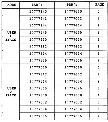
The concept of I and D space is used in mapping information into separate physical memory segments, depending on whether the information is considered instructions (I) or data (D). The use of I and D space allows programs to exist in two virtual segments and effectively doubles the address available to the user from 64 Kbytes to 128 Kbytes.
The 11/73 has the capability for I and D space whereas the 11/23 does not. To implement this feature, many more PAR/PDR pairs are necessary. The 11/73 has 48 PAR/PDR pairs, the 11/23 has only 16 PAR/PDR pairs.
GENERAL PURPOSE REGISTER SETS
The 11/23 and all previous LSI-11 processors have 1 set of general purpose registers, RO thru R7. Some of these are used for special purposes. R7 is used as the progri~m counter and R6 is used as the stack pointer. Internal to the 11/23 are 2 registers used for stack pointers, one for each processor mode). There are 5 additional registers RO thru RS.
The 11/73 has two sets of general purpose registers, listed in the table below. Only eight are visible to the user at any given time. There are two groups of six registers (RO thru RS and RO' thru RS'). The group currently being used is selected by bit 11 in the Processor Status Word (PSW). Only one stack pointer is visible to the user at anyone time and is determined by bits 14 and 15 in the PSW.
Register Number
o
Designation RO RO'1
2 3
4 5 6
7
R1 R1'
R2 R2'
R3 R3'
R4 R4'
RS RS'
KS]? SSP PC
KSP - Kernel Stack Pointer SSP - Supervisor Stack Pointer USP
=
User Stack PointeruNOTE # 006 Page 4 of 8
FLOATING POINT INSTRUCTION SET
Both the 11/23 and the 11/73 use the FP11 Floating Point Instruction Set., The FP11 Instruction Set is an option for the 11/23 (choice of either the KEF11 chip or the FPF11 floating point accelerator). The FP11 instruction set is part of the J11 microprocessor microcode and is therefore a standard feature of the 11/73.
LINE TIME CLOCK REGISTER
The original dual height 11/23 CPU does not have an LTC (Line Time Clock) register on the board. In 11/23 based systems the BDV11 boot module contains the LTC reg. In order to enable or disable LTC
interrupts under software control, the 11/23 must write to this register over the Q-bus.
11/23
1
7 5 4 6 Q-bus
LTC REG
The 11/73 has an LTC register on the CPU board. This means that whenever the 11/73 wants to enable or disable LTC interrupts under software control it writes to this on-board register. The address of the LTC register (location 177546) is 'trapped' on the board and NEVER goes out onto the Q-bus. When the 11/73 is used in a system with a BDV11, i t is recommended that software control over the LTC interrupts be disabled on the BDV11 (see uNOTE #114).
11/73
177546
I
Q-bus
ON-BOARD CACHE MEMORY
uNOTE # 006 Page 5 of 8
cache maintains copies of portions of main memory in very high-speed RAM and thus reduces access times significantly.
The 11/73 is the first Q-bus processor to implement a cache memory system. The cache is automatically enabled on power-up and its operation is transparent to software. However software can enable or disable the cache by writing to the Cache Control Register (CCR).
When the cache is enabled, any information fetched from main memory will be 'cached' i.e. placed in the high-speed RAM. Information fetched from an I/O device will NOT be 'cached' (i.e. information fetched from an address in the I/O page).
CAUTION: Digital Equipment Corporation does not support a system which uses shared or dual-ported memory on the Q-bus. However there are applications and non-DEC add-on hardware which do support such configurations. Consider the following:
The system below uses an 11/73, has a certain amount of main memory as well as dual-ported memory. The cache is enabled and the following sequence of events occur:
1. The 11/73 reads a word from the dual-ported RAM at address A which contains the value X. The value is
'cached'.
11/73
I
A: A: X
<---X
RAM
<l
Dual-Ported
EXTERNAL DEVICE
RAM
2. The external device writes a new value, Y, into location A.
11/73
A: A: X
Y
RAM
<---
EXTERNAL DEVICEuNOTE
#006
Page 6 of 8
is
in the
cache
and therefore uses the 'old' value of X.
But this is incorrect since
the
external device
updated
location A with the new value Y.
This anomaly can be corrected in a number of ways.
A.
Put the dual ported RAM somewhere in the I/O page since any I/O page
reference
always
bypasses
cache.
If the amount of dual-ported RAM is
large this may not be practical.
B.
The
memory
management
unit contains
several
page
Descriptor
Registers
(PDRs).
The
PDRs
contain
information
relative
to page
expansion, page length and access control.
Bit 15 of each PDR
is the
Bypass Cache bit.
If the PDR accessed during a relocation operation has
this bit set the reference will go directly to main memory.
Hits on
reads
or writes will
result
in
invalidation of the accessed cache
location.
Enabling this bit in each PDR associated with
the dual-ported memory
will force these references to bypass cache.
C.
Whenever the processor reads from the dual-ported RAM,
add
extra
code which will simply turn off the cache prior to the read and turn the
cache back on after the read is complete.
Turning the cache on and
off
can
be
done
by
setting the
appropriate bits in the Cache Control
Register.
PIPELINED PROCESSING
The 11/73 gets much of its performance by implementing a
prefetch and
predecode
mechanism.
The
major
benefit of
this
is that memory
references are overlapped with
internal operations which
results
in
faster
program execution.
The
11/23 does
not
implement
such
a
mechanism.
CAUTION
This
implementation
is completely compatible with DEC
hardware
and
software.
However
there are
applications and non-DEC
add-on hardware which may
be
confused.
Such
situations are
easily
corrected.
The prefetch mechanism assumes sequential program flow; one
instruction
immediately
follows
the
next.
Whenever
the program
flow
is not
sequential (i.e.
the PSW, CCR, PC or any memory management register
is
written)
the
pipeline
is 'flushed'.
If a non-DEC device does its own
'macro' memory management, the instruction flow may be confused.
For example :
uNOTE
*
006 Page 7 of 8time. This is done via a ROM set enable CSR. Assume the boot code in ROM set X is executing. Instruction X + 1 is a MOV instruction to the ROM enable CSR to transfer program control to ROM set Y. The intent of the ROM code is for statement Y + 2 in ROM set 2 to be executed next.
This will work OK with an 11/23. However because of the prefetch
mechanism of the 11/73, the 11/73 '~ill execute instruction X + 2 of ROM set 1, NOT ROM set 2.
This particular boot method effectively does its own memory mapping and since i t is done at the 'macro' level and external to the J11 cpu, the
pipeline is not 'flushed'. A simple solution is to include a NOP
instruction after the instruction which updates the ROM enable CSR, or to use a branch instruction which effectively changes the PC and causes the pipeline to be 'flushed'.
11/73
Sequence of events : 1. ROM X is enabled.
2. Instruction X + 1 enables ROM Y.
3. Next instruction to be executed is Y + 2.
User Boot ROM X
X X + 1 X + 2
X + n
~OM
Enable CSRDevice
Y
Y + 1 Y + 2
Y + n
MAP SIGNAL ON THE Q-BUS (UBMAP L)
ROM Y
The 11/23 outputs the signal UBMAP onto the Q-bus. Some non-DEC add-on equipment may use this signal for special purposes. This signal is not
defined by the Q-bus specification and for design reasons was not
included on the 11/73. Therefore, the 11/73 may not work with non-DEC devices which expect to see this signal.
ADDITIONAL INSTRUCTIONS AVAILABLE
These 3 instructions are part of the 11/73 instruction set but are NOT found in the 11/23:
CSM TSTSET WRTLCK
Call to Supervisor Mode
Test Destination and Set Low Bit
~NOTE # 006 Page 8 of 8
ADDITIONAL CPU REGISTERS AVAILABLE
ThE~ following CPU registers are part of the DCJ11 chip or implemented on the 11/73 module and are not found on the 11/23.
CPU Error Register
Memory System Error Register Cache Control Register
Hit/Miss Register
Additional PAR/PDR's necessary to implement I & D Space Program Interrupt Request Register
Line Time Clock Register (previously discussed) Maintenance Register
PROCESSOR SPEED
uNOTE
*
007 Title: User Defined Memory Maps For The Falcon Date: 01-MAY-84And The Falcon plus
Originator: Jack Toto Page 1 of 13
The memory maps on the Falcon, and E~alcon Plus are defined by the FPLA (Field Programmable Logic Array) that is located on board in socket XE41. This micronote explains how to redefine the existing maps.
The equipment needed to custom build the FPLA is as follows: 1. Signetics NS82S100N FPLA.
2. Signetics NS82S100N FPLA worksheet.
3. PROM programmer that supports Si9netics NS82S100N FPLA. 4. User written routine to convert binary into hex form,
needed for the PROM programmer.
The Falcon or Falcon Plus can be configured to anyone of four standard memory maps. When you custom build the memory map FPLA, you may keep this ability to select anyone of four memory map schemes, however i t is not nessecary to build in the four maps, you may build an FPLA with only one map for the Falcon. Further thE! addresses of the SLUs and Parallel I/O Port can be be changed to some other addresses on the module, or they can be relocated off the modulE! to some other device such as an MXV11-A/B, DLV11-J, DRV11-J, etc.
The memory map is defined by:
1. Selecting a range of addresses, for example addresses 077777 - 037777. This includes selecting the addrE!SSeS of the boards SLUs and PIO.
2. Asserting or deasserting the bits which define that range. 3. Defining which one of four memor)' maps the selected range of
addresses will respond.
4. Selecting an enable bit (A7 -AO), which tells the T-11 where to
find that range of addresses: on the Q-bus, on board the Falcon plus in one of the two sockets, or i.n the local RAM.
uNOTE i 007 Page 2 of 13
Below is an example of an FPLA worksheet that was completed specifying one map (map 0) which maps all of memory to the O-bus, and changes the address of SLU2 from 176540 - 176547, to 176500 - 176507. This format is simalar to the Signetics FPLA worksheet. For each address range shown, the combination of bits set (H), cleared (L), or in the don't care state (-) define that range. Further each address range has associated with it an output enable bit (A) that identifies the location of the memory containing that range. It is possible to define larger or smaller ranges then the ones shown here, if needed. More examples are provided in the Falcon Plus User's Guide Appendix H.
THIS IS AN FPLA MAP FOR COMPANY: XYZ
ADDRESS RANGE 177600-177777 177570-177577 .177560-177567 .177540-177557 177500-177537 .177400-177477 177000-177377 .176600-176777 .176560-176577 .176550-176557 176540-176547 .176510-176537 .176500-176507 .176400-176477 176300-176377 176240-176277 176220-176237 176210-176217 176200-176207 176000-176177 .174000-175777 170000-173777 160000-167777 140000-157777 100000-137777 000000-077777
x
X RAM OS OLO OS OB OB OB OB OB OS OB OS OL1 OB OB OB OB OS PIO OS OS OS OS OS OS OBI I I I I I I I I I I I I I I I
000 001 0 1 0 1 010 1 0 1 7 8 6 9 5 0 4 1 322 3 1 5 0 4 1 1 1 1 1 1 0 0 0 0 0 0 0 0 0 0 5 4 321 0 9 8 7 6 543 2 1 0 H H H H H H
-- -- -- H H H H H L H H H H - - - H H H H H L H H H L H H H H H L H H L -- -- -- H H H H H L H L H H H H H L L H H H H L
H H H L H H H H H L H L H H H -- -- -- H H H L H L H H L H - - - H H H L H L H H L L - - - H H H L H L H L - H - - - H H H L H L H L L L H H H L H L L
H H H L L H H -- -- -- H H H L L H L H
H H H L L H L L H -- -- -- H H H L L H L L L H - - - H H H L L H L L L L H H H L L L
-- - - H H L - - - -
-- H L
- - - L - - -
-H -H L - - -
-H L - - - - L
-L -L L L L L L L L L L L L L L L L L L L
L L
L L L L L L L L L L L L
L L
L L L L L L L L L L L L L L L L
H H H H H H H H H H H H H H H H H H H H H H H L L L
F F F F F F F
7 6 5 4 321 0
A A A A A A A A A A A A A A A A A A A A A A A A A A
7 6 5 4 321 0
uNOTE # 007 Page 3 of 13
Once the address ranges have been coded, they need to be converted into the formatted file shown directly below. This file will be used as the input file to a program (see end of Micronote) that will output the FPLA terms in a format that is usable by the PROM Programmer itself. When converting the above worksheet to FPLA terms, the following should be considered:
1. The area at the beginning of the file may be used as a comment area as long as the word "START" is not used in the comments. "START" is the key word to begin'the formatting process while the word "END" is the key word used to signal the formatter that the processing must be terminated. Both words MUST appear in capital letters.
2. The layout of the map must be as follows:
115 114 113 112 III 110 109 lOa 107 106 105 104 103 102 101 100 07 06 05 04 03 02 01 00
TERM1
115 114 113 112 III 110 109 loa 107 106 105 104 103 102 101 100
I
TERM2 07 06 05 04 03 02 01 00Where 115 is input 15 on the FPLA ,114 is input 14 on the PLA etc. further 07 is output 7 on the FPLA and 06 is output 6 on the PLA.
3 II " - " indicates a "DON'T CARE ON 'I'HAT INPUT" AND
*
indicates a "DON'TCARE ON THIS OUTPUT".
The following is the formatted FPLP.. map for the worksheet shown above. Notice that bus address bit 00 is translated to FPLA bit 114, that bus address 01 is translated to FPLA bit 100, that is, the bus address bits are not directly translated to the FPLA bits, however the worksheet activity (output) bits F7 - FO translate directly to FPLA bits A7 - AO. START
LH--HHH---HHH--L
A*******
LHHHHHH---HHLHHL
*****A**
LHHHHHH---HHLHLL
**A*****
LHLHHHH---HHLH-L
*****A**
LH-HHHH---HHLL-L
*****A**
LH-LHHH---HHL--L
*****A**
LH--LHH---HH---L