Søren Ulstrup,1 Antonija Grubiˇsi´c ˇCabo,2 Deepnarayan Biswas,3 Jonathon M. Riley,3 Maciej Dendzik,2 Charlotte E. Sanders,2 Marco Bianchi,2 Cephise Cacho,4 Dan Matselyukh,4 Richard
T. Chapman,4 Emma Springate,4 Phil D. C. King,3 Jill A. Miwa,2 and Philip Hofmann2
1Advanced Light Source, E. O. Lawrence Berkeley National Laboratory, Berkeley, California 94720, USA 2
Department of Physics and Astronomy, Interdisciplinary Nanoscience Center, Aarhus University, 8000 Aarhus C, Denmark 3SUPA, School of Physics and Astronomy, University of St. Andrews, St. Andrews, United Kingdom
4Central Laser Facility, STFC Rutherford Appleton Laboratory, Harwell, United Kingdom (Dated: January 5, 2017)
The semiconducting single-layer transition metal dichalcogenides have been identified as ideal materials for accessing and manipulating spin- and valley-quantum numbers due to a set of favorable optical selection rules in these materials. Here, we apply time- and angle-resolved photoemission spectroscopy to directly probe optically excited free carriers in the electronic band structure of a high quality single layer (SL) of WS2grown on Ag(111). We present a momentum resolved analysis of the optically generated free hole density around the valence band maximum of SL WS2 for linearly and circularly polarized optical excitations. We observe that the excited free holes are valley polarized within the upper spin-split branch of the valence band, which implies that the photon energy and polarization of the excitation permit selective excitations of free electron-hole pairs with a given spin and within a single valley.
In two-dimensional (2D) materials, control of the spin-and valley-degrees of freedom has been suggested as a new type of tuning knob for carrier dynamics [1]. Single-layer (SL) transition metal dichalcogenides (TMDCs) such as SL MoS2 and WS2 are particularly promis-ing candidates for new spin- and valley-tronic device paradigms, owing to the broken inversion symmetry of their crystal lattices, a strong spin-orbit coupling and a direct band gap at the ¯K and ¯K0 valleys in the elec-tronic structure [2–4]. These properties have been in-directly verified in SL TMDCs through selective exci-tation of bound electron-hole pairs with circularly po-larized light, leading to the observation of valley polar-ized excitons [5–8], which could be coherently manipu-lated [9]. Device measurements have shown indications of spin- and valley-coupled photocurrents [10] and Hall effects [11, 12]. Direct measurements of the electronic structure and associated quasiparticles have been carried out for the bulk TMDC material WSe2 using photoe-mission spectroscopies with spin [13] and time resolu-tion [14]. Such measurements can, to some degree, even give information about the situation in a single layer, due to the surface sensitivity of photoemission spectroscopy. However, there is a need for experimental evidence and quantification of these properties for free carriers in the electronic structure of actual SL TMDCs, which are truly non-inversion symmetric materials.
Time- and angle-resolved photoemission spectroscopy (TR-ARPES) is a powerful experimental approach for de-tecting optically excited free carriers with time-, energy-and momentum-resolution with extremely high sensitiv-ity towards 2D materials [15, 16]. In this technique, a pump pulse with tuneable photon energy and polariza-tion optically excites the material in quespolariza-tion. The ex-cited state is then probed by ARPES with an ultraviolet
pulse, produced via high harmonic generation (HHG), which can provide sufficiently high photon energies to reach the ¯Kvalleys at the corner of the SL TMDC’s Bril-louin zone (BZ). Since the two pulses are time-delayed with a resolution on the order of 30 fs, it is possible to stroboscopically record the ultrafast dynamics in the band structure of the material [17, 18]. In the context of SL TMDCs, such experiments have focused on the size of the screening- and free carrier-induced quasiparticle gap renormalization on various types of substrates [19, 20]. A SL TMDC with strong spin-orbit coupling is desirable for a TR-ARPES experiment that endeavors to directly detect free carriers selectively excited in the spin-split states in a given valley [21]. We therefore use epitax-ial SL WS2 grown on Ag(111). WS2 is characterized by a strong spin-splitting on the order of 420 meV at the valence band maximum (VBM) [22]. Intriguingly, our experiments reveal excited electron and hole populations that are strongly peaked for a resonant excitation be-tween the upper VB spin state and the conduction band (CB). A significant valley polarization of free carriers de-velops under these conditions when we pump the material with circularly polarized light.
Eq. Exc. Diff.
Intensity
(arb. u.) 0
2.00 2.45 Diff.
1.6 1.3 1.0
k (Å-1)
3 2 1 0 -1
Ebin
(eV)
Eq.
1.6 1.3 1.0
k (Å-1)
pos
neg min
max
(a) (b)
(d)
0
upper VB
lower VB
Summed Intensity
Diff. (arb. u.)
t (fs) -400 0 400
τ = (100 50) fs +− CBM
VBM
2 1 0 -1
Ebin (eV)
Intensity
Diff. (arb. u.)
(c)
3 2 1 0 -1
Ebin
(eV)
hνpump = 2.05 eV
K K
hνpump = 2.05 eV
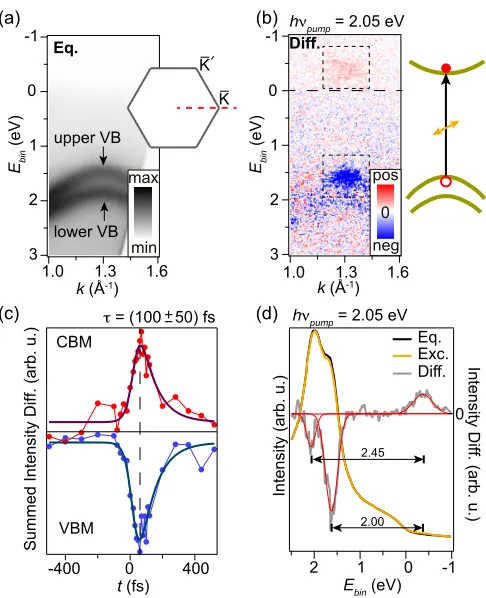
FIG. 1: (Color online) (a) ARPES spectrum of WS2 taken before optical excitation. The BZ in the inset shows the mea-surement direction via the dashed line. (b) Difference between the peak excitation spectrum obtained with an s-polarized pump pulse at a photon energy of 2.05 eV and the equilibrium spectrum in (a). The sketch presents the resonant excitation at the VBM and CBM. (c) Time dependent intensity differ-ence (markers) summed over the dashed boxed regions on the CBM and VBM, respectively, in (b). Overlaid thick lines are fits to a function consisting of an exponential rising edge and a single exponential decay with time constant τ. (d) Inte-grated EDCs at equilibrium (Eq.) and peak excitation (Exc.) along with their difference (Diff.) for the corresponding data in (b). The integration was carried out over the VBM and CBM in the momentum range from 1.15 ˚A−1 to 1.45 ˚A−1. Gaussian fits of the peaks in the difference are shown along with estimates of the transition energies in eV (error bars are
±0.05 eV).
was used for HHG in an Ar gas cell. We used a harmonic with a photon energy of 25 eV for ARPES. A tuneable pump pulse was achieved by seeding an optical paramet-ric amplifier (TOPAS), enabling an optical excitation en-ergy (wavelength) of 2.05 eV (605 nm). The polarization of the pump pulse was controlled with a quarter wave-plate, which could be rotated with a motor in order to switch betweens-, σ−- and σ+-polarization, permitting measurements with all three polarizations. The fluence of the pump pulse was kept around 3.0 mJ/cm2in order to obtain maximum pump-probe signal while avoiding space-charge effects [24]. The average acquisition time
for pump-probe data was 24 hours. We used variable exit slit settings for the probe pulse and entrance slit sizes of the SPECS Phoibos 100 electron analyzer depending on the statistics required for the measurement, such that the energy resolution varies between 150-350 meV. The an-gular and time resolution were on the order of 0.2◦ and 40 fs, respectively. The temperature of the sample was kept at 70 K during measurements.
In Fig. 1(a) we present the electronic structure of our SL WS2 sample around the ¯K-valley, measured by ARPES along the direction of the BZ shown in the inset. The spectrum was obtained in equilibrium conditions be-fore the arrival of the optical excitation. Clearly resolved spin-split bands of the VBM are observed in the spec-trum. Throughout the paper we refer to the band on the lower (higher) binding energy side as the upper (lower) VB. The effect of pumping can be best seen in the dif-ference between the spectrum in the excited state and the equilibrium spectrum in Fig. 1(a). This difference is taken at a time delay corresponding to the peak of the excitation (t = 30 fs). Excitation with an s-polarized pump pulse with a photon energy of 2.05 eV leads to a population of excited holes and electrons in the upper VB and conduction band minimum (CBM), which is seen via the blue and red contrast, respectively, in the differ-ence spectrum in Fig. 1(b). The time dependdiffer-ence of the observed difference signals reveals a symmetric and ul-trafast decay of excited carriers in the CBM and VBM regions with a time constant τ of 100 fs, as shown in Fig. 1(c). Slightly different pump energies were used to establish the resonant condition between VBM and CBM (not shown) and these dynamics are found to be independent of the pump pulse energy within our time resolution. This time-dependence reflects the coupling of the SL WS2 to the underlying metallic substrate, which efficiently drains optically excited free carriers, as previ-ously observed for SL MoS2 on Au(111) [19]. Since the time-dependence of the carrier relaxation is dominated by the coupling to the substrate, we will focus on the conditions of the carrier excitation process. The analy-sis in Fig. 1(d) presents the integrated energy distribu-tion curves (EDCs) for the equilibrium and excited state spectra along with their difference. Gaussian fits of the peaks in the difference reveal how the upper and lower VBs and the CBM line up. We find a direct quasiparticle gap at ¯Kof (2.00±0.05) eV, confirming that our choice of pump pulse energy of 2.05 eV is essentially resonant with the transition between the upper VB and the CBM. The quasiparticle gap energy is somewhat smaller than the average value of 2.43 eV calculated for freestanding SL WS2 in the GW approximation [25], which is fully consistent with an expected screening-induced band gap renormalization by the metal substrate [19, 26].
[image:2.612.56.299.50.349.2]Intensity
Diff. (arb. u.)
0
2 1 0 -1
Ebin (eV) 1.6
1.3 1.0 1.6 1.3 1.0
Diff. Diff.
3 2 1 0 -1
Ebin
(eV)
k (Å-1) k (Å-1)
K K
domain 1
domain 2 K
K
K K
(a) (b) (c)
(d) (e) (f)
σ- σ+
σ- σ+
σ -σ+
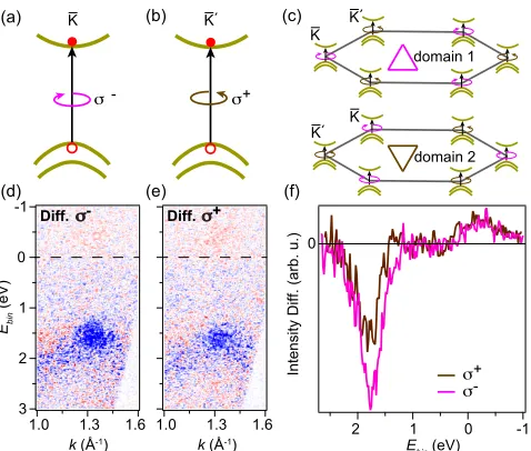
FIG. 2: (Color online) (a)-(b) Selection rules for transitions from the upper VB to the CBM in the ¯K and ¯K0 valleys. (c) BZ orientations and selection rules for the two possible domain orientations probed in this work. (d)-(e) Difference signal for optical pumping with (d) σ− and (e) σ+ circular polarization and a photon energy of 2.05 eV. (f) EDCs of the difference integrated over the VBM and CBM regions for the data in (d)-(e).
pulses, carriers are exclusively excited in the upper VB at ¯K(see Fig. 2(a)), while forσ+-polarized pump pulses carriers are exclusively excited in the upper VB at ¯K0 (see Fig. 2(b)). In the present case of an epitaxial WS2 layer grown on Ag(111), the substrate symmetry permits the existence of mirror domains [27], implying that we are measuring a superposition of the two BZs with the valleys swapped, as shown in Fig. 2(c). Regardless of these domains, our experiment reveals a stronger deple-tion of the upper VB intensity when we use pump pulses withσ−-polarization. This is seen via the comparison of
the intensity difference for the excited holes in the VB generated by σ−- andσ+-polarized pulses in Figs. 2(d) and 2(e) and the integrated EDCs of the difference for both polarizations in Fig. 2(f). Note that the existence of mirror domains does not necessarily imply an equal distribution of domain types and even single domain ori-entations can be achieved in similar systems, depending on the growth conditions [28].
In order to obtain a quantitative estimate of the op-tically induced free hole density we proceed with a band-resolved line shape analysis of the VBM region. EDCs around the VBM of the spectra obtained with an s-polarized optical excitation are fitted with two Lorentzian line shapes on a parabolic background, as shown in Fig. 3(a). The fitted Lorentzian components of the spin-split VBs are extracted as shown in Fig. 3(b), and we observe a good agreement between the experi-mental dispersion in Fig. 3(c) and the fitted dispersion
Intensity
(arb. u.)
2 1
Ebin
(eV)
K EDC analysis
k (Å-1)
1.19
k = 1.32 Å-1
Lorentzian fit
(a) (b)
Exp. Fit
Exp. Eq. Exp. Exc. Fit Eq. Fit Exc.
2 1
Ebin (eV) 2Ebin (eV) 1
Eq. Diff.
1.28 1.37 1.46
(c)
(d)
(e)
(f) 2
1
Ebin
(eV)
Exp.
Fit Fit
Exp.
K
FIG. 3: (Color online) (a) EDCs extracted over the VBM and fitted with two Lorentzian line shapes on a parabolic back-ground. Each EDC is binned over a range of±0.02 ˚A−1. (b) Example EDC fit for equilibrium (Eq.) and optically excited (Exc.) data with plots of the individual Lorentzian compo-nents. (c) Measured spectrum used for the EDC analysis in (a). (d) Reconstruction of the spectrum using the fitted EDCs. (e)-(f) Difference (Diff.) spectra corresponding to the data and fit in (c)-(d). The spectrum analyzed here was measured with ans-polarized optical excitation at a photon energy of 2.05 eV (see also Fig. 1(b)).
in Fig. 3(d). The fit captures position and amplitude changes in the line shape, which could occur due to gap renormalization and optically excited holes, respectively. Comparisons of the Lorentzian fits in Fig. 3(b) and the difference spectra in Figs. 3(e) and 3(f) show that the main change in the excited spectrum relates to an am-plitude change in the upper VB. This can be translated into a number for the excited holes,Nh, per momentum
state by integration of the fitted Lorentzian components, normalization to the spectral weight in the equilibrium spectrum, and finally conversion of the normalized spec-tral weight in the excited spectrum to a value for Nh
[20].
Results of the above analysis are compared for the var-ious pump pulse polarizations in Fig. 4, which shows the distribution of optically excited holes around the VBM. We fit the momentum dependence of Nh with
a hole-like Fermi-Dirac function fh(k) = 1−fe(k) =
1−1/{exp[((k−k0)−µ)/δ] + 1} in the cases where Nh > 0 is clearly fulfilled. Here (k) is the bare
dis-persion of either the upper or lower VB, which is deter-mined from the EDC fits of the band positions in Fig. 3, and{k0, µ, δ} constitute the set of fitting parameters
that determine the position, height and width of the dis-tribution. The fits of the Fermi-Dirac distribution show that the variation inNh(k) corresponds to a thermalized
[image:3.612.58.297.51.254.2] [image:3.612.318.566.55.206.2]( ) ( )
k (Å-1) k (Å-1)
0.10
0.05
0.00
nh < 1010/cm2
Nh,
upper VB
nh = 5.0 (1011/cm2)
1.5 1.3
1.1
nh = 6.6 (1011/cm2)
nh = 3.3 (1011/cm2)
0.10
0.05
0.00
1.5 1.3
1.1
nh < 1010/cm2
nh < 1010/cm2 (b)
(a)
(d) (c)
σ
-σ+
Nh,
lower VB
Nh,
upper VB
Nh,
lower VB
K K K K
K K K K
[image:4.612.55.301.49.297.2]s-pol s-pol
FIG. 4: (Color online) (a)-(d) Number of holes Nh per momentum state (markers) and distribution function fits (curves) for (a)-(b) s-polarized optical pumping and (c)-(d) circularly polarized optical pumping with a photon energy of 2.05 eV. The hole number was extracted using the analysis procedure in Fig. 3 for (a), (c) the upper VB and (b), (d) the lower VB. The calculated hole density nh per valley is provided in each panel. The insets of the WS2band diagrams present the possible transitions for the optical excitation con-ditions in each panel.
valley,nh [20]. The detection limit fornh in this type of
analysis is estimated to be 1010 holes per cm2. We note that the above band-resolved analysis of optically excited hole numbers fully relies on the momentum resolution of TR-ARPES, and that it directly reveals that the excited hole populations in SL WS2are consistent with thermal-ized Fermi-Dirac functions at the ultrashort timescales, within 40 fs of optical excitation, studied here.
In Fig. 4(a) we observe that s-polarized resonant pumping at the upper VB generates a clear distribution of holes in this band compared to the lower VB, as seen in Fig. 4(b). This general trend can be understood from the simple schematics of the excitation processes shown in the insets of Figs. 4(a)-(b). Resonant pumping from the upper VB leads to free electrons and holes, which are situated at the band edges where the phase space for intra-band decay processes is small, thereby making the optical pumping efficient at generating free carriers. Pumping at this photon energy with circularly polarized pulses leads to a twice as large optically generated hole density in the upper band using σ−- compared to σ+ -polarization, as seen in Fig. 4(c). No significant hole density is detected in the lower band in Fig. 4(d), which is consistent with the result fors-polarized pump pulses
with the same energy in Fig. 4(b). The observation of a moderate free carrier density usingσ+-polarization can be attributed to co-existing mirror domains in the sample and a deviation in the pump-pulse polarization from perfect circular due to the geometry constraints of the experiment. Our analysis shows that, even under these circumstances, it is possible to excite a surplus of free carriers in the ¯K-valley of epitaxial WS2 grown on a metal surface. Since these carriers all derive from the upper band they are also characterized by a single spin quantum number.
Our results reveal that the level of control of the spin-and valley-degrees of freedom demonstrated for excitons in SL TMDCs also extends to optically generated free carriers in these materials. We expect this scheme is transferable to arbitrary substrates and other SL TMDC materials.
We thank Phil Rice for technical support during the Artemis beamtime. We gratefully acknowledge fund-ing by VILLUM FONDEN via the Centre of Excellence for Dirac Materials (Grant No. 11744), the Aarhus University Research Foundation, EPSRC (Grant Nos. EP/I031014/1 and EP/L505079/1) and The Royal Soci-ety. Ph. H., J. A. M. and S. U. acknowledge financial sup-port from the Danish Council for Independent Research, Natural Sciences under the Sapere Aude program (Grant Nos. DFF-4002-00029, DFF-6108-00409 and DFF-4090-00125). Access to the Artemis Facility was funded by STFC. Data underpinning this publication can be ac-cessed at
[1] A. Rycerz, J. Tworzydlo, and C. W. J. Beenakker, Nature Physics3, 172 (2007).
[2] D. Xiao, G. Liu, W. Feng, X. Xu, and W. Yao, Physical Review Letters108, 196802 (2012).
[3] K. Mak, C. Lee, J. Hone, J. Shan, and T. Heinz, Phys. Rev. Lett.105, 136805 (2010).
[4] Q. Wang, K. Kourosh, A. Kis, J. Coleman, and M. Strano, Nature Nanotechnology7, 699 (2012). [5] H. Zeng, J. Dai, W. Yao, D. Xiao, and X. Cui, Nature
Nanotech.7, 490 (2012).
[6] K. Mak, K. He, J. Shan, and T. Heinz, Nature Nanotech-nology7, 494 (2012).
[7] T. Cao, G. Wang, W. Han, H. Ye, C. Zhu, J. Shi, Q. Niu, P. Tan, E. Wang, B. Liu, et al., Nature communications 3(2012).
[8] Q. Wang, S. Ge, X. Li, J. Qiu, Y. Ji, J. Feng, and D. Sun, ACS Nano7, 11087 (2013).
[9] A. M. Jones, H. Yu, N. J. Ghimire, S. Wu, G. Aivazian, J. S. Ross, B. Zhao, J. Yan, D. G. Mandrus, D. Xiao, et al., Nature Nanotechnology8, 634 (2013).
[10] H. Yuan, X. Wang, B. Lian, H. Zhang, X. Fang, B. Shen, G. Xu, Y. Xu, S.-C. Zhang, H. Y. Hwang, et al., Nat
Nano9, 851 (2014).
[12] X. Xu, W. Yao, D. Xiao, and T. F. Heinz, Nat Phys10, 343 (2014).
[13] J. M. Riley, F. Mazzola, M. Dendzik, M. Michiardi, T. Takayama, L. Bawden, C. Granerod, M. Leandersson, T. Balasubramanian, M. Hoesch, et al., Nature Physics 10, 835 (2014).
[14] R. Bertoni, C. W. Nicholson, L. Waldecker, H. H¨ubener, C. Monney, U. D. Giovannini, M. Puppin, M. Hoesch, E. Springate, R. T. Chapman, et al., arXiv:1606.03218 pp. 1–8 (2016).
[15] J. C. Johannsen, S. Ulstrup, F. Cilento, A. Crepaldi, M. Zacchigna, C. Cacho, I. C. E. Turcu, E. Springate, F. Fromm, C. Raidel, et al., Phys. Rev. Lett.111, 027403 (2013).
[16] I. Gierz, J. C. Petersen, M. Mitrano, C. Cacho, I. C. E. Turcu, E. Springate, A. St¨ohr, A. K¨ohler, U. Starke, and A. Cavalleri, Nature Mater.12, 1119 (2013).
[17] L. Perfetti, P. A. Loukakos, M. Lisowski, U. Bovensiepen, H. Eisaki, and M. Wolf, Physical Review Letters 99, 197001 (2007).
[18] T. Rohwer, S. Hellmann, M. Wiesenmayer, C. Sohrt, A. Stange, B. Slomski, A. Carr, Y. Liu, L. M. Avila, M. Kallane, et al., Nature471, 490 (2011).
[19] A. Grubiˇsi´c ˇCabo, J. A. Miwa, S. S. Grønborg, J. M. Riley, J. C. Johannsen, C. Cacho, O. Alexander, R. T. Chapman, E. Springate, M. Grioni, et al., Nano Lett.15, 5883 (2015).
[20] S. Ulstrup, A. Grubiˇsi´c ˇCabo, J. A. Miwa, J. M. Riley, S. S. Grønborg, J. C. Johannsen, C. Cacho, O. Alexander,
R. T. Chapman, E. Springate, et al., ACS Nano10, 6315 (2016).
[21] S. Ulstrup, J. C. Johannsen, F. Cilento, J. A. Miwa, A. Crepaldi, M. Zacchigna, C. Cacho, R. T. Chapman, E. Springate, S. Mammadov, et al., Phys. Rev. Lett.112, 257401 (2014).
[22] M. Dendzik, M. Michiardi, C. Sanders, M. Bianchi, J. Miwa, S. Grønborg, J. Lauritsen, A. Bruix, B. Ham-mer, and P. Hofmann, Phys. Rev. B92, 245442 (2015). [23] F. Frassetto, C. Cacho, C. A. Froud, I. C. E. Turcu,
P. Villoresi, W. A. Bryan, E. Springate, and L. Poletto, Optics Express19, 19169 (2011).
[24] S. Ulstrup, J. C. Johannsen, F. Cilento, A. Crepaldi, J. A. Miwa, M. Zacchigna, C. Cacho, R. T. Chapman, E. Springate, F. Fromm, et al., J. Electron Spectrosc. Relat. Phenom.200, 340 (2015).
[25] F. A. Rasmussen and K. S. Thygesen, The Journal of Physical Chemistry C119, 13169 (2015).
[26] A. Bruix, J. A. Miwa, N. Hauptmann, D. Wegner, S. Ul-strup, S. S. Grønborg, C. E. Sanders, M. Dendzik, A. Grubiˇsi´c ˇCabo, M. Bianchi, et al., Phys. Rev. B93, 165422 (2016).
[27] O. Lehtinen, H.-P. Komsa, A. Pulkin, M. B. Whitwick, M.-W. Chen, T. Lehnert, M. J. Mohn, O. V. Yazyev, A. Kis, U. Kaiser, et al., ACS Nano9, 3274 (2015). [28] F. Orlando, P. Lacovig, L. Omiciuolo, N. G. Apostol,