Built-In Reliability Design of a High-Frequency
SiC MOSFET Power Module
J. Li, E. Gurpinar, S. Lopez-Arevalo, A. Castellazzi
Power Electronics, Machines and Control GroupUniversity of Nottingham Nottingham, UK
L. Mills
Semelab TT-Electronics Lutterworth, UK [email protected]Abstract— A high frequency SiC MOSFET-based three-phase, 2-level power module has been designed, simulated, assembled and tested. The design followed a built-in reliability approach, involving extensive finite-element simulation based analysis of the electro-thermo-mechanical strain and stress affecting the switch during both manufacturing and operation: structural simulations were carried out to identify the materials, geometry and sizes of constituent parts which would maximize reliability. Following hardware development, functional tests were carried out, showing that the module is suitable for high switching frequency operation without impairing efficiency, thus enabling a considerable reduction of system-level size and weight.
Keywords— SiC MOSFET, multi-chip power modules, reliability.
I. POWER MODULE DESIGN
A 1.2 kV SiC-MOSFET based three-phase half-bridge power module was designed, specifically for avionic applications, where improved gravimetric and volumetric power density and efficiency are highly appreciated.
The structure of one phase switch is shown in Fig. 1, with indication of assembly layers and location of interconnection pins. Each switch allocates two SiC MOSFETs, which are soldered on the substrate top metallization (Sub_Metal_Top in Fig. 1 b)) together with the power and drive terminals (S-Pins); the substrate bottom metallization is soldered onto the module base-plate. All the solder joints are made of eutectic tin-silver (Sn-3.5Ag) solder of constant 100 m thickness. Because this module does not target specifically high-temperature applications, aluminum (Al) bond-wire were used for interconnections to the device top-side, with diameter of 125 m.
Two types of substrates commonly used in the construction of power modules have been considered, namely Aluminum-Nitride (AlN) and Silicon-Nitride (Si3N4). Table I summarizes the main characteristics of
interest for the two materials: Si3N4 has higher flexural
strength than AlN and is thus typically processed in thinner layers than AlN for use in building power modules; this also implies that, although Si3N4 has a
lower thermal conductivity than AlN, the equivalent
thermal resistance of the substrates is comparable if the difference in thickness is taken into account. Here, both experiment and simulations are used to inform the choice on most reliable solution.
a)
[image:1.595.307.537.669.757.2]b)
Fig. 1. One-phase SiC switch: a) top view, b) side view.
TABLEI
Preliminary experimental testing was carried out on batches of the two types of assemblies, with different thicknesses of copper tracks deposited onto them. The tiles were subjected to passive thermal cycling and Cu tracks detachment/peel-off was used as an indication of failure. The results are summarized in Table II and give a clear indication that Si3N4 tiles can withstand a much
higher number of cycles before degradation and failure intervenes. Also, it is interesting to note that the thicker the Cu tracks, the shorter the number of cycles to failure.
TABLEII
SIMULATION CASES WITH CONSIDERATION OF SUBSTRATES AND BUMP SHAPES
I. BUILT-IN RELIABILITY ANALYSIS
Finite element (FE) modeling and simulation are employed to investigate the effects of the type and the thickness of substrate and base plate used on the entity of the maximum thermo-mechanical stress and its distribution. Simulations target the analysis of the thermal and thermo-mechanical performance of the assembled power module. The considered simulation cases are listed in Table III.
TABLEIII
SIMULATION CASES WITH CONSIDERATION OF SUBSTRATES AND BUMP SHAPES
No Sub Ceramic Thickness Sub Metal Bot Thickness Sub Metal Top Thickness Base Plate Thickness
A1 1 mm AlN 0.3 mm Cu 0.4 mm Cu 3 mm AlSiC-9 A2 1 mm AlN 0.3 mm Cu 0.4 mm Cu 3 mm AlSiC-12 A3 1 mm AlN 0.3 mm Cu 0.4 mm Cu 2 mm AlSiC-9 A4 0.635 mm AlN 0.3 mm Cu 0.4 mm Cu 2 mm AlSiC-9 A5 0.635 mm AlN 0.2 mm Cu 0.3 mm Cu 2 mm AlSiC-9 A6 0.635 mm AlN 0.3 mm Cu 0.3 mm Cu 2 mm AlSiC-9 B1 0.3 mm Si3N4 0.3 mm Cu 0.4 mm Cu 3 mm AlSiC-9
B2 0.3 mm Si3N4 0.3 mm Cu 0.4 mm Cu 3 mm AlSiC-12
B3 0.3 mm Si3N4 0.3 mm Cu 0.4 mm Cu 2 mm AlSiC-9
B4 0.3 mm Si3N4 0.2 mm Cu 0.3 mm Cu 3 mm AlSiC-9
B5 0.635 mm Si3N4 0.3 mm Cu 0.4 mm Cu 2 mm AlSiC-9
B6 0.635 mm Si3N4 0.2 mm Cu 0.3 mm Cu 2 mm AlSiC-9
B7 0.635 mm Si3N4 0.3 mm Cu 0.3 mm Cu 2 mm AlSiC-9
The first one is 0.4mm and 0.3mm thick active brazed Cu on both sides of 1 mm or 0.635mm thick AlN tile. The second one is 0.4 mm and 0.3mm thick or 0.3mm and 0.2mm active brazed Cu on both sides of 0.3mm or 0.635mm thick Si3N4 tile, respectively. Also, two types
of base plate materials have been considered: AlSiC-9 and AlSiC-12 composites. For each of the two composites, two thicknesses of 3 mm and 2 mm for the Base_Plate were selected and compared in order to reduce the stress/strain accumulation within the solder joints.
The characteristics of the material used for the solder layer, Lead (Pb)-Tin (Sn)-Silver (Ag) solder of the composition 62Pb36Sn2Ag, are summarized in Table IV.
TABLEIV SOLDER PROPERTIES
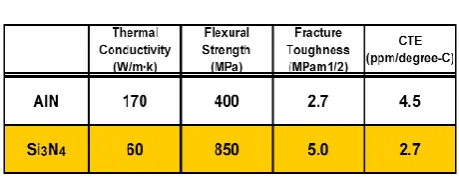
Modeling and simulation were carried out using well-established commercially available tools (e.g., Abaqus, Ansys). Fig. 2 a) shows the numerical structural model (meshed) of the switch: the largest brick element is 0.5×0.5×1.5mm, and the smallest is 0.5×0.25×0.025mm. Here, the largest brick element is 0.5×0.5×1.5mm, and the smallest is 0.5×0.25×0.025mm. S4R shell elements of 0.5×0.5mm or 0.5×0.25mm in size were also used to discretize the nickel-phosphorous (NiP) finishing on the surfaces of the substrates, and in both the Al and Ni metallization on two sides of the MOSFETs respectively.
The assembly was first subjected to a predefined temperature profile of 221°C down to 25°C for 3 min to simulate the stress and strain developed during the reflow process. In this stage, all the Al wire bonds were deactivated and therefore no strain/stress was developed on them. Power losses of one MOSFET are shown in Fig. 2 b). These losses were considered as heating sources to simulate the thermal performance of the assembly during a realistic mission profile. They were also taken in account in the heat exchange boundary condition. For this boundary condition, a heat exchange coefficient of 5000W m-2 K-1 was applied to the bottom surface of the
used to describe the mechanical properties of both the Cu and Al. The properties of Al were applied to both the Al wire bonds and the Al metallization on the front side of the MOSFETs. Anand’s creep model was used to describe the mechanical properties of the Sn-3.5Ag solder alloy.
a)
b)
Fig.2. a) Representative meshing system to discretize the designed switch module. b) Power loss of one MOSFET during a realistic mission profile.
II. THERMO-MECHANICAL SIMULATION
For all simulation cases during the mission profile, the highest junction temperature was observed on one MOSFET at 23.01s. The simulation shown is mainly concerned with the stress and strain developed in all solder joints. Simulation results reveal that the maximum von Mises stress in the solder joint between the substrate and the base plate are larger than those in the two solder joints used for attaching the two SiC MOSFETs on the substrate. The maximum creep strain accumulation in the former solder joint is significantly larger than that in the latter two solder joints after the first cycle of the mission profile. However, and depending on the simulation cases, the maximum creep strain accumulation in the former solder joint may be higher or lower than that in the latter two solder joints after the second cycle of the mission
profile.
Fig. 3 shows the von Mises stresses and creep strains obtained from simulations in all the solder joints for case A1 after two cycles of the mission profiles. Table V compares the simulation cases for the highest junction temperatures of the MOSFETs and the maximum von Mises stress and creep strain developed in the solder joint between the substrate and the base plate. In Table V, TJ,max is for the highest junction temperature of the
MOSFETs during the mission profile; Smax0, Smax1 and
Smax2 represent the maximum von Mises stress and max0,
max1 and max2 represent the maximum creep strain in the
solder joint of the as-reflowed assembly and the same one after one and two cycles of the mission profile; and max1=max1-max0, max2=max2-max1.
a)
[image:3.595.71.274.166.505.2]b)
Fig. 3. Simulation results of (a) von Mises stresses and (b) creep strains within all solder joints for simulation case A1 after two cycles of the mission profile.
According to these results, the best design is achieved when the base-plate is 2mm thick AlSiC-9 and the substrate is AlN-based with 0.635mm thick AlN tile (case A4). In this case, the highest junction temperature of the MOSFET is only 0.6C higher than that in simulation case A1; however, the maximum creep strains and creep strain accumulations dominating the reliability of the critical solder joint in the module would be significantly lower than those in the other simulation cases.
[image:3.595.326.524.282.578.2]TABLEV
COMPARISON OF THE HIGHEST JUNCTION TEMPERATURES OF THE MOSFETS AND THE MAXIMUM VON MISES STRESS,CREEP STRAIN AND CREEP STRAIN ACCUMULATION IN THE SOLDER JOINT BETWEEN THE SUBSTRATE AND BASE PLATE FOR THE 13SIMULATION CASES
Case TJ,MAX (K)
Smax0
(MPa) (MPSmax1A)
SMAX2
(MPa)
MAX0
(%)
MAX1
(%)
MAX2
(%)
MAX1
(%)
MAX2
(%)
A1 363.2 42.6 39.5 38.9 12.65 13.40 13.84 0.75 0.44
A2 363.9 44.2 41.6 40.7 18.84 19.67 20.17 0.83 0.50
A3 363.8 41.0 38.2 37.6 6.87 7.25 7.52 0.37 0.27
A4 363.8 41.3 37.9 37.4 6.83 7.10 7.23 0.27 0.13
A5 365.6 41.3 38.6 38.1 7.65 8.13 8.41 0.48 0.28
A6 364.8 40.8 37.9 37.4 7.07 7.35 7.49 0.28 0.14
B1 366.4 42.6 39.1 38.4 10.96 11.80 12.26 0.84 0.46
B2 367.4 44.2 40.5 39.9 16.79 17.66 18.12 0.87 0.46
B3 367.6 41.3 38.1 37.6 7.32 7.70 8.01 0.38 0.31
B4 368.7 43.0 39.6 41.2 12.10 12.88 13.32 0.78 0.44
B5 370.6 42.5 39.0 38.4 8.98 9.61 9.98 0.63 0.37
B6 373.4 42.4 39.5 39.0 10.25 10.88 11.27 0.63 0.39
B7 372.6 42.5 39.0 38.4 9.17 9.81 10.19 0.64 0.38
simulation results using AlN and Si3N4 (e.g., case A1 in
comparison with case B3), Si3N4 substrates were retained as the best solution for built-in reliability module development.
III. HARDWARE DEVELOPMENT AND TEST
A. Development
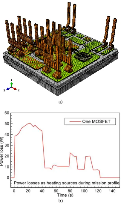
Fig. 4 a) shows details of the assembled switches and module. The module of Fig. 4 b) was later filled with a silicone-based dielectric material to provide the required isolation and insulation. Finally it was fully encapsulated by using a plastic lid leading to the final product of Fig. 4 c). The final module as assembled for both functional and reliability testing weighs 126.5g ±0.5g. In view of the specified goal of lightweight development, this is a very satisfactory results, competitive with presently upcoming commercial solutions. A noteworthy feature of the module is the complete separation of the power and driving terminals and current loops. All power terminals were finally implemented with single connectors, doubled to reduce parasitic inductance and enable high switching frequency. The module has been subjected to both functional testing in inverter operation and to temperature cycles for technology validation. Here, the results of functional testing are reported to demonstrate the high frequency capability and good thermal performance. Reliability tests are still ongoing at the time of submission.
B. Test
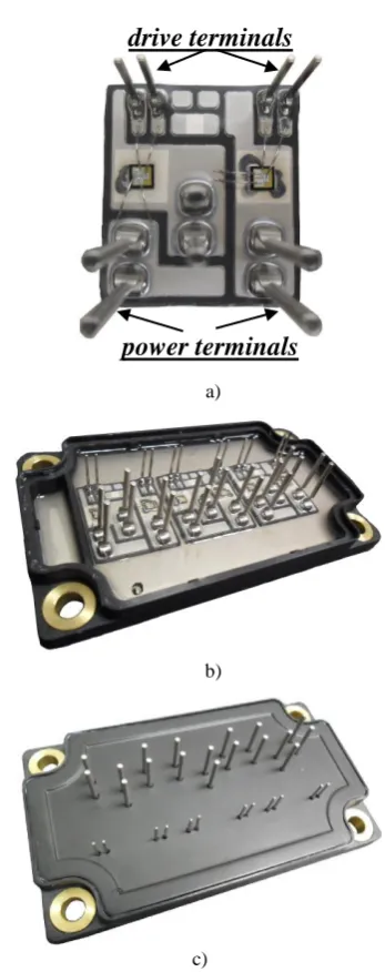
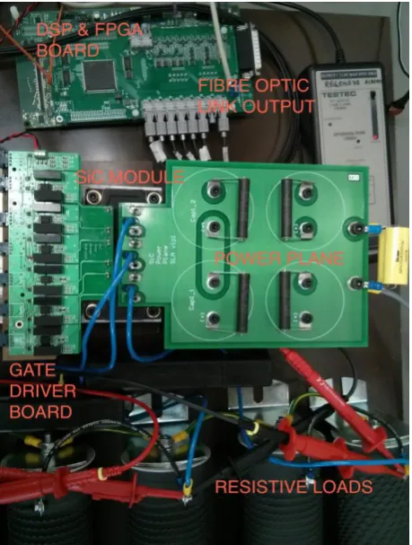
A flexible test setup was designed to test a number of modules that have been manufactured . The setup comprises of four electrolytic capacitors (350V, 3.3mF each) with discharge and balancing resistors (47kΩ each), and the SiC module power pins are mounted directly onto the power plane. The schematic is shown in Fig. 5. Fig. 6 shows a picture of the test setup.
a)
b)
[image:4.595.332.506.292.731.2]c)
Fig. 4. Assembled switches a), full power module b) and encapsulated device c).
drive terminals
Fig. 5. Schematic of the test circuit.
Fig. 6. Photograph of the test set-up.
The inverter was tested in open loop; the necessary PWM drive signals are generated by a DSP and FPGA control platform with programmable dead-time values. The PWM signals are transmitted to a gate driver board, which is mounted directly onto the SiC module gate pins, through fiber optic cables in order to minimize the noise interference at high switching
[image:5.595.57.287.349.653.2]frequencies. An isolated gate drive IC supplies +22V to turn-on and -3.1V to turn-off each individual SiC MOSFET. The input DC link voltage is 540V to represent the DC bus in an avionic systems. The inverter was tested at full load (6kW) and half load (3kW) conditions. The output inductive filter was 3 mH. Output phase-to-neutral RMS voltage is set to 115V with 50Hz fundamental frequency. Tests were run at increasing switching frequencies: 5, 10, 20, 40, 60, 80 and 100 kHz. Fig. 7 shows the three phase current components for a switching frequency of 5 kHz.
Fig. 7. Phase current waveforms at a switching frequency of 5 kHz.
The output phase voltage and current, and the drain-source (Vds) and gate-source voltage (Vgs) waveforms of
[image:5.595.309.535.481.643.2]a)
[image:6.595.69.278.66.385.2]b)
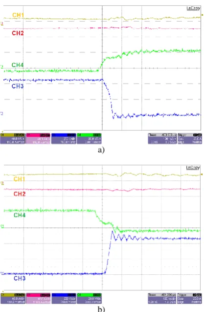
Fig. 8. Turn-on, a), and turn-off waveforms, b), at fsw=100 kHz,
full-load (CH1 and CH2: Current in phase A and B, 40A/div, CH3:Vds=250V/div, CH4:Vgs=20V/div, timebase=100ns/div).
In a final test, we removed altogether the inductive filter from the load. Fig. 9 shows the output current waveforms of all three phases at full load and 100 kHz switching frequency in this condition. Although the load at the output of the converter is purely resistive, due to leakage inductance at the output cables and resistors, and high switching frequency, the output phase currents become continuous. Clearly, the ripple is not contained, but these measurements give a very clear indication of the dramatic reduction in inverter volume and size which can be enabled by the high-frequency SiC power module.
Fig. 9. Output current waveforms at fs=100 kHz, full-load
(CH1= Phase A current 15 A/div, CH2= Phase B current 15 A/div, CH3= Phase C current 15A/div, timebase= 2ms/div).
Finally, Fig. 10 reports the measured efficiency at full load as a function of the switching frequency. A decrease of only 2.5% (i.e., 15 W) is measured for a twentyfold increase in the switching frequency (from 5 to 100 kHz), which is directly attributed to the SiC device characteristics [4].
Fig. 10. Efficiency curve of power module at 6 kW output power.
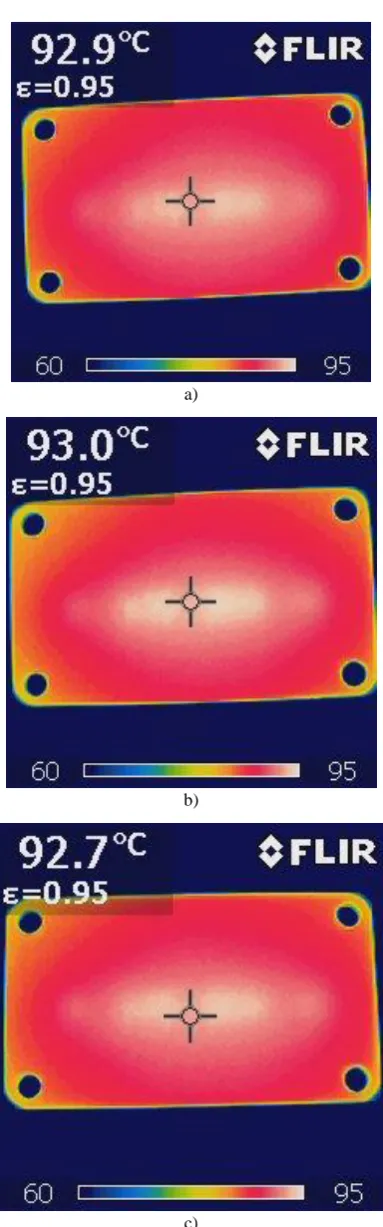
To complete experimental characterization, the SiC power module was dismounted from the heat-sink and the temperature at the baseplate was measured under different operational conditions. To avoid failure, the maximum allowed baseplate temperature was around 90 ºC. This corresponded to the following test conditions: POUT=2.5 kW at
fs=5kHz and POUT=1.5kW at fs=40 and 80 kHz. The
baseplate temperature distribution corresponding to these test conditions is given in Fig. 11 a), b) and c) . All results highlight a very even temperature distribution, with maximum at the center in line with the expectations, and the capability of the module to work properly and efficiently with noticeable base-plate temperatures, that is, minimum cooling requirements, at high switching frequencies and power levels.
IV. CONCLUSION
In this paper, the design, the thermo-mechanical modeling using finite element analysis and, simulation and experimental results of a lightweight SiC MOSFET module are presented. Simulation results using finite element suggests that the best design is obtained when the Base_Plate is based on AlSiC-9 with a thickness of
[image:6.595.311.535.155.295.2] [image:6.595.69.278.585.725.2]module must be regarded as a solution enabling optimum trade-off choices in inverter development.
a)
b)
c)
Fig. 11. Infrared thermal mapping of the module baseplate under different operational conditions: POUT=2.5 kW and
fs=5kHz, a); POUT=1.5kW at fs=40 kHz, b);
POUT=1.5kW at fs=80 kHz, c).
REFERENCES
[1] A. Zeanh et al., “Thermo mechanical modelling and reliability study of an IGBT module for an aeronautical application.” In Proc. 9th Int. Conf. on Thermal, Mechanical and Multiphysics Simulation and Experiments in Electronics and Micro-Systems, EuroSimE 2008.
[2] A. Zeanh et al., “Lifetime and reliability assessment of AlN substrates used in harsh aeronautic environments power switch modules”, Advanced Materials Research vol. 112, pp 113-127, 2010.
[3] W.W. Sheng, R.P. Colino, “Power Electronic Modules: Design and Manufacture”, CRC Press LLC, Florida, USA,
2005.
[image:7.595.77.269.96.711.2]