The morphological characterisation of grains and grain
boundaries.
MUIRHEAD, John J.
Available from Sheffield Hallam University Research Archive (SHURA) at:
http://shura.shu.ac.uk/20099/
This document is the author deposited version. You are advised to consult the publisher's version if you wish to cite from it.
Published version
MUIRHEAD, John J. (2001). The morphological characterisation of grains and grain boundaries. Doctoral, Sheffield Hallam University (United Kingdom)..
Copyright and re-use policy
CITY CAMPIUS, HOWARD STREET SHEFFIELD S1 1VYB
\ ° n i 3
ProQuest Number: 10697406
All rights reserved
INFORMATION TO ALL USERS
The quality of this reproduction is dependent upon the quality of the copy submitted.
In the unlikely event that the author did not send a complete manuscript and there are missing pages, these will be noted. Also, if material had to be removed,
a note will indicate the deletion.
uest
ProQuest 10697406
Published by ProQuest LLC(2017). Copyright of the Dissertation is held by the Author.
All rights reserved.
This work is protected against unauthorized copying under Title 17, United States Code Microform Edition © ProQuest LLC.
ProQuest LLC.
789 East Eisenhower Parkway P.O. Box 1346
The Morphological Characterisation of Grains and
Grain Boundaries
John Muirhead
A thesis submitted in partial fulfilment of the
requirement of Sheffield Hallam University for the
degree of Doctor of Philosophy
Declaration
The work described in this thesis was carried out by the author in the Materials
Research Institute, Sheffield Hallam University, between October 1997 and
October 2000. The author declares that this work has not been submitted for
any other degree. The work is original except where acknowledged by
reference.
Author:
John Muirhead
Supervisor:
Abstract
ACKNOWLEDGEMENTS
To my supervisory team, Dr Jess Cawiey, Dr Colin English, Prof John
Titchmarsh and Prof Andrew Strang, I would like to extend my gratitude for
allowing me to tap into their wisdom. I would particularly like to acknowledge
the support, unfaltering advice and constant concern to get me through this
PhD from Jess, my director of studies. Also to Colin, my first industrial
supervisor, for his encouragement and for showing confidence in me.
Steve Porter, once a technician at Sheffield Hallam University who played an
important part in creating this thesis, was a friend with an invaluable level head
at times of ‘crisis’ and a great many thanks go to him. To the rest of the
technicians, Paul Slingsby and Cheryl Shaw and the IT manager Terry Hudson,
thanks for the support and good sense of humour.
A special thanks go to my parents, for once again backing me up 100% for
what I want to do, for pushing me to the end and especially for always being
there to listen. To the rest of my family I thank for their encouragement and for
helping me to enjoy the good times.
Last but by no means least I would like to acknowledge the constant support
and love of my girlfriend, Bex, for making the ‘downs’ ‘ups’ and especially for
her unique ability to ‘gently’ persuade me to keep going and get this thesis
Table of contents
1 .INTRODUCTION_______________________________________ 1
1.1.General introduction 1
1.2.The nature of polycrystalline materials 2
1.3.The objectives of the programme 3
1.4.The experimental approach 5
1.4.1. Specimen preparation 5
1.4.2. Manual methods. 6
1.4.3. Automatic image analysis. 6
1.4.4. Electron Back Scatter Diffraction 7 2.LITERATURE SURVEY__________________________________ 8
2.1. Introduction 8
2.2.Microscopy 8
2.2.1. Automatic image analysis 8
2.2.2. Electron Backscattered Diffraction 11
2.2.2.1.Introduction 11
2.2.2.2.A description of the technique 13
2.2.2.3.Resolution 14
2.2.2.4.Lattice strain 18
2.2.2.5.Further limitations of EBSD 19 2.2.2.6.A comparison of other techniques 20 2.3.The nature of polycrystalline materials 23
2.3.1. Complex microstructures 23
2.3.1.1.Introduction 23
2.3.2. Grain boundaries 23
2.3.2.3.Coincident site lattice 24
2.3.2.4.The influence of grain
boundaries on microstructure 25 2.3.2.5.High and low angle boundaries 29 2.3.2.6.The influence of grain boundaries
2.3.2.7.Special boundaries 35
2.4.Specimen preparation techniques 37
2.4.1. Etching 37
2.5.Grain size measurement methods 39
2.5.1. Comparison of ASTM E112 methodologies 39 2.5.1.1.Intercept methods against planimetric 39 2.5.1.2.Intercept against comparison 40
2.5.1.3.An overall comparison 41
2.5.2. Comparison of standards 41
2.5.2.1.Summary 46
2.5.3. ASTM E112 47
2.5.4. Problems with grain size measurement 49
2.5.4.1.Distributions 50
2.5.4.2.Twinning 51
2.6.Summary 51
3. EXPERIMENTAL_______________________________________ 52
3.1. Introduction 52
3.2.Specimen preparation 52
3.2.1.The mild steel 52
3.2.2.Why specimen preparation was so important 58
3.2.3.Techniques investigated 61
3.2.3.1.Etching 62
3.2.4.Summary of preparation techniques 64 3.2.5.Mixed pearlite ferrite material 67
3.3.Methods of grain size measurement 68
3.3.1 .The ASTM grain size number 68
3.3.2.Manual methods 70
3.3.2.1 .Comparison chart method 70
3.3.2.2.The planimetric method 71
3.3.2.3.Intercept methods 72
3.4.Automatic image analysis 75
3.4.2.1.Image convolution processes 79
3.4.2.2.Edge detection 80
3.4.2.3.Thresholding 83
3.4.3.Grain size measurement methods 88
3.5 Missing boundaries and grain size measurements 89 3.5.1. The impact of missing boundaries on grain size
measurements 90
3.5.2.The location of missing boundaries 92
3.5.2.1.Magnification selection 92
3.6.Electron Back Scatter Diffraction (EBSD) 94
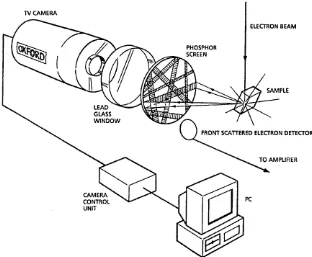
3.6.1 .System set up 94
3.6.2.Formation of EBSD patterns 96
3.6.3.Interpretation of EBSD Patterns 99 3.6.3.1.Automatic pattern indexing 100
3.6.4.Crystal orientations 104
3.6.4.1.Misorientations 105
3.6.5.EBSD examination procedure 106
3.6.5.1.Calibration 106
3.6.5.1.Collection of electron backscatter
patterns 110
3.6.5.3.Resolution and mapping times 111
3.6.6.Sources of error 114
3.6.6.1.Orientation measurement 114
3.7.Image distortion on the SEM 116
4.RESULTS_____________________________________________ 118
4.1 .Specimen preparation 118
4.1.1.Results 120
4.2.Grain size measurements 128
4.2.1 .Inter-comparison of manual methodologies 129 4.2.1.1.Effect of increasing fields 132
4.2.2.Sampling 135
4.2.2.1.The number of specimens 135
4.2.2.3.Number of counts per field 141 4.2.3.The impact of missing boundaries on grain size
measurements 142
4.2.3.1.Manual measurements 143
4.2.3.2.Automatic image analysis 146
4.2.4.Comparison of automatic image analysis grain size
measurements with EBSD 149
4.2.4.1.Comparison of results with boundaries
removed 171
4.2.5.Comparison of two optical grain size measurements 176 4.2.6.The impact of not including the boundary into the
measurement using the automatic image analysis
system 180
4.2.7.The grain shape and misorientation of missing
boundaries 185
4.2.8.Comparison of manual and automatic grain size
measurements with optical and EBSD imaging 189 4.2.8.1 .A comparison of results from optical and
EBSD imaging using manual methods 192 4.2.8.2.A comparison of results from using manual
and automatic methods 193
4.3.Assessment of boundaries with misorientation 194 4.3.1 .Assessment with the location of boundaries on
EBSD but not reconstructed on optical 194 4.4.The misorientation of grains and grain size 197
4.4.1.Misorientation data for grain boundaries between
large/large, large/small and small/small grains 200 4.4.2.Misorientation and grain size for specimen
5.DISCUSSION 205
5.1.Introduction 205
5.2.Grain size methodology 206
5.2.1 .Inter-comparison of manual methodologies 206
5.2.2.Sampling 211
5.2.2.1.Summary 212
5.3 The impact of missing boundaries on grain size
measurements 214
5.3.1.Summary 217
5.4.Assessment of the impact of image resolution on
grain size measurements using automatic image analysis. 218 5.4.1.Differences between the EBSD images of different
resolutions 219
5.4.1.1.Summary 221
5.4.2.Differences between the optical and the lower pixel
resolution EBSD images for grain size 222 5.5.Comparison of the results from the two operators 229
5.5.1.Assumptions made in the reconstructing of the
optical images by two different operators 233 5.5.2.Boundaries found in one image form but not in the
other 235
5.5.2.1.Boundaries that existed in the optical images
but not in the EBSD images 236
5.5.2.2.Boundaries that existed in the EBSD images but not in the optical images
(missing boundaries) 237
5.6.Missing boundaries and misorientation 240 5.6.1 .A summary of the results from using automatic
image analysis 241
5.7.Comparison of manual and automatic grain size
the EBSD and optical images 244 5.7.2.Differences between manual and automatic
measurements of the EBSD and optical images 246
5.7.2.1.Summary 250
5.8.Misorientation data for grain boundaries between
large/large, large/small and small/small grains 252 5.8.1 .The association of misorientation and grain size 252
6.CONCLUSIONS 254
6.1.Grain size methodology 254
6.1.1.Inter-comparison of manual methodologies 254 6.1.2.Sampling for grain size measurements 254 6.1.3.The choice of manual grain size measurement
methods 255
6.2.The impact of missing boundaries on grain size
measurements 256
6.3.The impact of pixel resolution on grain size
measurements using automatic image analysis 257 6.3.1.Grain sizes of EBSD images of different pixel
resolutions 257
6.3.2.Grain sizes of optical images and lower pixel resolution
EBSD images 258
6.4.The decisions regarding reconstructing grain boundaries 259 6.4.1.Boundaries reconstructed in one image form but not
in the other 259
6.5.Manual measurements of EBSD and optical images 260 6.5.1.Manual and automatic measurements of EBSD and
optical images 260
6.6.Missing boundaries and misorientation angles 262 6.7.Misorientation angles of grain boundaries between
7. FUTURE WORK 264
7.1.Grain size measurements 264
7.2.Automatic image analysis 265
7.3.Electron back scatter diffraction 267
8 POSTERS. PUBLICATIONS AND REFERENCES_________ 268
8.1 posters 268
8.2 publications 268
List of figures
Figure 1
Figure 2 Figure 3 Figure 4 Figure 5 Figure 6 Figure 7 Figure 8 Figure 9
Figure 10
Figure 11 Figure 12
Figure 13 Figure 14
Figure 15
A schematic of the location of the areas
measured in the cross-section of the mild steel A schematic of the location of the areas
measured in the longitudinal section of the mild steel Images of EBSD maps without using a
suspension in the specimen preparation (left image) with using a suspension (right image).
A plot showing the conversion from the number of grains per mm squared and mean linear intercept values to G grain size units.
Images demonstrating the error imposed from adding a boundary to an object
The Sobel Convolution Filters
A digital image of the mild steel and the same
image after the Sobel filter has been passed through Image demonstrating how grain boundary
reconstruction can produce grains that are too large (left) and too small (right)
Binary Images showing 0% (left) and 20% (right) missing boundaries.
The hardness indentations providing markers for four segments to be montaged.
Components of an EBSD system
A schematic showing the formation of one pair of Kikcuhi lines from the diffraction of the electron beam with one family of lattice planes.
EBSD pattern from the mild steel
A plot demonstrating how lines are defined in Hough space.
A plot showing all the vectors representing a line
Figure 16
Figure 17
Figure 18
Figure 19
Figure 20 Figure 21 Figure 22 Figure 23 Figure 24 Figure 25 Figure 26
A comparison of the distances between indentations between images taken at specimen at zero tilt and images at 70 tilt
An image of the specimen after polishing with Buehler's Gamma Micropolish No 3 Alumina B and etching using a 2% nital solution.
An image of the specimen after polishing with Struers’ OP, an Acidic Alumina, made up with 50% water and then etched with ferric chloride.
An image of the specimen after polishing using Struer's Colloidal Silica and etching using a 2% nital solution
An image of the specimen after using the Buelher's Gamma Micropolish No 3 Alumina B and 20% volume ferric chloride mixture.
An image of the specimen after using Buehler’s Gamma Micropolish No 3 Alumina B and a 5% nital polish/etch mixture
An image of the specimen after using the
Buehler’s Gamma Micropolish No 3 Alumina B and a 10% nital polish/etch mixture
An image of 2 specimens after using the
Buehler’s Gamma micropolish No 3 Alumina B and a 7% nital polish/etch mixture.
A plot of the ASTM grain size numbers for each specimen and for each method
A plot showing the effect of increasing the
number of fields measured on the grain size number A plot of the percentage relative accuracy
Figure 27 Figure 28 Figure 29 Figure 30 Figure 31 Figure 32 Figure 33 Figure 34 Figure 35 Figure 36 Figure 37
A plot of the ASTM G number from each specimen from using the lineal and planimetric
methods 136
A plot of the ASTM G numbers of the lineal
method against the planimetric method 137 A plot of the individual ASTM G numbers from
each field of view in each specimen using the lineal
method 139
A plot of the individual ASTM G numbers from each field of view in each specimen using the
planimetric method 139
A histogram of the mean ASTM G numbers from measuring 1,2 and 3 fields of view using the lineal
method 139
A histogram of the mean ASTM G numbers from measuring 1,2 and 3 fields of view using the
planimetric method 139
A plot of the ASTM G number measured on
images with 0,5,10,15 and 20% boundaries removed
using all the manual methods 143
A plot of the mean of the manual methods measuring the ASTM G number on images with 0,5,10,15 and
20% boundaries removed 145
A plot of the ASTM G number measured on
images with 0,5,10,15 and 20% boundaries removed measuring with the single circle, lineal and 3 circle
method using the automatic image analysis system 146 A plot of the mean ASTM G number from
measuring with the single circle, three circle and lineal methods using the automatic image analysis system on images with 0,5,10,15 and 20% boundaries removed 147
Figure 38 Figure 39 Figure 40 Figure 41 Figure 42 Figure 43 Figure 44 Figure 45 Figure 46 Figure 47 Figure 48
An Optical image of specimen 1 with the
measured grains colour coded according to their size 152 An EBSD image of the smaller pixel resolution of
specimen 1 with the grains measured colour coded
according to their size 152
An EBSD image of the greater pixel resolution of specimen 1 with the grains measured colour coded
according to their size 153
A histogram of the grain area distributions measured on the optical and EBSD images of both pixel
resolutions using the automatic image analysis
system for specimen 1 154
An Optical image of specimen 2 with the measured
grains colour coded according to their size 156 An EBSD image of the smaller pixel resolution of
specimen 2 with the grains measured colour coded
according to their size 156
An EBSD image of the greater pixel resolution of specimen 2 with the grains measured colour coded
according to their size 157
A histogram of the grain area distributions measured on the optical and EBSD images of both pixel resolutions using the automatic
image analysis system for specimen 2 158 An Optical image of specimen 3 with the measured
grains colour coded according to their size 160 An EBSD image of the smaller pixel resolution of
specimen 3 with the grains measured colour coded
according to their size 160
An EBSD image of the greater pixel resolution of specimen 3 with the grains measured colour coded
Figure 49 Figure 50 Figure 51 Figure 52 Figure 53 Figure 54 Figure 55 Figure 56
A histogram of the grain area distributions measured on the optical and EBSD images of both pixel resolutions using the automatic image analysis system for specimen 3
An Optical image of specimen 4 with the measured grains colour coded according to their size
An EBSD image of the smaller pixel resolution of specimen 4 with the grains measured colour coded according to their size
An EBSD image of the greater pixel resolution of specimen 4 with the grains measured colour coded according to their size
A histogram of the grain area distributions measured on the optical and EBSD images of both pixel resolutions using the automatic image analysis system for specimen 4 A histogram of the grain area distributions measured on the optical and EBSD images of both pixel resolutions using the automatic image analysis system for all specimens Flistograms of grain area distributions of each individual specimen comparing measurements on the optical images, the EBSD images of greater pixel resolution and the optical images with those boundaries not on the EBSD images removed
Figure 57 Figure 58 Figure 59 Figure 60 Figure 61 Figure 62 Figure 63 Figure 64 Figure 65 Figure 66
Flistograms of grain area distributions of each individual specimen comparing measurements on the optical images reconstructed by two operators (operator 1 & operator 2) and the EBSD images of
greater pixel resolution. 178
Flistograms of grain area distributions of all specimens comparing measurements on the optical images
reconstructed by two operators (operator 1 & operator 2) and the EBSD images of greater pixel resolution. 179 The ratios of perimeter/area plotted against the
aspect ratios of minor/major axes of ellipses of the same
area 181
The ratios of perimeter/area plotted against the
area of the ellipses 183
A plot of the ASTM grain sizes measured on the optical and the greater pixel resolution EBSD images of each specimen using the planimetric, single circle, three circle and lineal manual methods and also by automatic image analysis 191 A histogram of the boundaries not reconstructed by Operator 1 categorised according to their misorientation
angles 194
A histogram of the boundaries not reconstructed by Operator 2 categorised according to their misorientation
angles 196
An example of a true grain identification map
showing a more refined grain structure 198 Examples of EBSD images with, from left to right,
small grains, small and large grains and large grains colour coded according to the scale shown above 199 A plot of the misorientation data for grain
boundaries between small/small, small/large and
Figure 67
Figure 68
Plots of the percentage of grain boundaries between small/small, small/large and large/large grains with
misorientation angles for specimens 3 and 4. 202 A schematic demonstrating the location and directions grain size measurements were conducted during
List of tables
Table 1
Table 2 Table 3 Table 4 Table 5 Table 6 Table 7 Table 8 Table 9
Table 10
Table 11
The elemental composition of the mild steel reference material
The mean linear intercept results from
measuring along the transverse cross sectional plane. The specific location of the measurement fields are shown in Figure 1.
The number of intercepts measured across a longitudinal section of the mild steel
The etches and their compositions investigated in determining the ideal specimen preparation technique.
The microscope settings for each manual grain size methodology
The compositions of the etches tested for the sample preparation of the mild steel.
The sample mean calculated from all fields of view across all specimens and methods. Showing the mean linear intercept values and the equivalent ASTM G numbers from measuring along 1 and 2 lines using the lineal method The image pixel sizes of the optical and the two EBSD images for all four specimens
Grain shape and misorientation data of boundaries in the EBSD images but not in the optical images (missing boundaries )for operator 1
Table 12
Table 13
Table 14
The mean sphericities and aspect ratios of the optical and the EBSD images of both pixel resolutions for all specimens
Showing the percentages of the total
number of boundaries measured in specimens 3 and 4 that are smaller than 15° and
greater/equal to 15° misorientation for each grain size category
Showing the percentages of the total
number of boundaries measured in specimens 3 and 4 that are smaller than 15° and
1. INTRODUCTION
1.1. General Introduction
This thesis is concerned with some of the methods currently available for
measuring the grain size in polycrystalline, metallic materials.
To be able to measure the size of grains with some confidence is important for
quality assurance and material property determination purposes and at the time
of writing there were four quantitative manual grain size measurement methods
prescribed in various industrial standards. Also, within the last few years with
the advent of faster and more economical computers the use of automatic
image analysis has played a more prominent role. All these techniques are
investigated within this thesis.
The metallographic preparation of specimens to reveal the microstructure is
important for subsequent grain size determination and involves many variables,
such as an incomplete network of grain boundaries. The impact of these
variables to the final grain size measurement is also investigated.
Electron back scatter diffraction (EBSD) is a technique that provides crystal
orientation information. This technique was adopted for this work to provide a
complete network of grain boundaries against which the location of missing
provide the misorientation data of boundaries allowing a relationship with grain
size to be investigated.
1.2. The Nature of Poivcrvstalline Materials
Most metallic materials are made up of crystals (polycrystalline), otherwise
known as grains, which are formed from conventional methods of metal
production. It is the mechanical working and thermal treatments through these
metal production methods that are responsible for the microstructures
developed. Each grain contains atoms, which are arranged in a systematic
manner and are defined by the Bravais lattice system. The planes and
directions of these atoms are described by using Miller Indices and
stereographic projections. The grains are often orientated differently to one
another and between them grain boundaries are formed, which define the
transition zone where the atoms rearrange from one grain orientation to
another. The orientation of the planes can influence certain properties of the
material [1].
It is also the size of the grain that is important when predicting certain material
properties, for example the Hall-Petch equation describes the relationship
between grain size and yield stress. This relationship can be described as the
Specifically the Hall-Petch relationship for steels is:
criys = A + B d'/2 Equation 1
where aiys is the lower yield stress, A is the friction stress opposing the
dislocation motion, B is a material constant which represents the ease of
generating dislocations, and d is the average grain diameter. [2,3,4]
1.3. The Objectives of the programme
The underlying objective of the programme was to establish better practice in
grain size measurements through a study of the methods that were in use at
the time of writing. There were various aspects considered and the specific
objectives were as follows:
1. To assess current practice of modern manual grain size measurement
methods through an inter comparison of those prescribed in the relevant
industrial standards. This was achieved by considering accuracy, e.g. the
number of grains, fields of view and specimens to reach a specific accuracy
level, and efficiency with respect to reaching this accuracy level by
minimising time and errors.
2. To assess the impact of missing boundaries on grain size measurements by
comparing the difference in the measured grain size of microstructures with
various percentages of boundaries removed against a specific accuracy
level. The location of grain boundaries is of course important when grain
size measurements are to be conducted since they define the shape and
size of the grains. However, locating a grain boundary using optical
microscopy is not always straightforward since they are often difficult to etch
using traditional chemical etching techniques. Often a reconstruction of so
called ‘missing boundaries’ is required prior to grain size measurement to
ensure that the microstructure is representative of the material.
Determining where a boundary might or might not have been etched is often
conducted visually by the operator and hence is subject to an individual’s
judgement. However, with the use of the EBSD technique a complete
network of boundaries was provided due to their location being determined
from the orientation of one grain relative to another (misorientation). Thus
by comparing a specimen area where images have been created via optical
microscopy and by EBSD the actual location of missing boundaries became
possible.
3. The use of automatic image analysis and digital images in grain size
measurements by considering the importance of pixel resolution and by
4. The relationship between grain size and misorientation angles through the
use of EBSD to provide a complete network of grain boundaries and the
misorientation data for each boundary.
1.4. The experimental Approach
1.4.1. Specimen preparation
A sample material was provided by Corns* being a mild steel with a fully ferritic,
equi-axed microstructure. The relative simplicity of this microstructure allowed
an investigation that is focused on grain size methods without complicating
factors such as multi-phases and directionality and it is relatively convenient for
etching and distinguishing boundaries.
The preparation of the material was important in terms of ensuring the surface
finish was representative of the bulk material. Etching of the surface was also
important in order to reveal the grain boundaries for subsequent reconstruction
using the automatic image analysis system and for measurement of grain size.
Specimen preparation was also important for the use of EBSD since the
information this technique provides came from very close to the surface.
Therefore, the residual stresses induced from specimen preparation had to be
eliminated and etching became important to this end.
Various specimen preparation techniques were investigated, including electro
chemical methods, until the optimum was developed.
1.4.2. Manual methods.
This material was extensively characterised for grain size using all the methods
prescribed in the standards BS4490 [5], IS0643 [6] and ASTM E112 [7] and by
using an automatic image analyser. Where appropriate a highly accurate grain
size measurement was established together with a substantial data set.
By characterising the sample material and from investigating the application of
grain size measurements within industry a critique of the standards was
conducted to investigate their suitability to meet the requirements within
industry.
1.4.3. Automatic image analysis.
An automatic image analysis system can conduct measurements on a digital
format and provide a large amount of data relatively efficiently compared to
manual measurements. A system was used to measure grain size, which
involved firstly capturing and digitising images of the microstructure. Thus the
use of digital imaging was incorporated within the work, specifically the
firstly involved reconstructing the boundaries by using standard image
processes and also by operator interfacing using digital editing.
1.4.4. Electron Back Scatter Diffraction
Electron back scatter diffraction is a scanning electron microscope (SEM)
based diffraction technique and the electron back scatter patterns produced are
used to determine crystal orientations. From the orientation of one grain with
respect to another, known as misorientation, the location of a grain boundary
was established. This provided a complete network of grain boundaries
compared to the uncertainty in the location of all the boundaries from etching
specimens and using optical imaging.
2. LITERATURE SURVEY
2.1. Introduction
The literature survey reported in this chapter is concerned with the current
situation regarding microscopy and material properties. The chapter begins
with a survey of microscopy, particularly involving automatic image analysis
and Electron Back Scatter Diffraction (EBSD). The use of automatic image
analysis for quantitative analysis of microstructures is assessed. The use of
EBSD as a tool for understanding complex material properties and their
microstructure is assessed in the next section. This is followed by a survey of
the specimen preparation techniques for the specific steels used in this thesis.
The final section provides a survey of grain size measurement methods,
including a critique of the most common standards in use within industry.
2.2. Microscopy
2.2.1. Automatic Image analysis
Vander Voort described the use of image analysis systems for grain size
measurement in [8]. ‘With the current drive to improve product quality, which
has fostered development of statistical databases, control charts, and so forth,
and in the required volume.’ Consequently ASTM devised a standard, namely
ASTM E1382, ‘Standard Test Methods for Determining Average Grain Size
Using Semi - Automatic and Automatic Image Analysis’ [9], which was
introduced in 1990 [8].
Leithner detailed the limitations of image analysis in grain size measurement
based upon the importance of specimen preparation [10]. The example given
was that a scratch could be counted as a boundary. Indeed automatic image
analysis of microstructure necessitates the most optimum specimen
preparation possible, e.g. no scratches from mechanical polishing [11,12].
As a comparison with manual image analysis Le Pennec et al set out to
measure grain size in a low carbon steel using image analysis [13]. It was
found that the ‘questionable reproducibility of manual methods is overcome.’ In
addition to this a relative error of the mean intercept of 1% or 2% was gained
allowing mechanical properties to be predicted with a level of accuracy ‘never
before reached’.
Another limitation of image analysis was defined by the resolution of the
camera and microscope, both limiting the overall imaging resolution. For
example, the measurement of a grain can be influenced by the number of
pixels making up a boundary, where fewer pixels result in a less accurate
measurement. Thus image analysis is more ‘sensitive to magnification
Mishima conducted a more critical assessment [16], where an attempt was
made to determine how consistent results were if several different image
analysis systems were used to measure the grain size of a common sample.
Essentially the investigation involved creating binary images by thinning an
input image, repairing the grain network, and finally measuring. Thinning was
required before measurements could be undertaken to maximise the grain area
by minimising the grain boundary. Several specimen preparation methods
were used to assess the systems’ abilities further. The conclusion drawn was
that for microstructures containing complexities such as precipitate dispersion
input images ‘cannot go through the grain boundary thinning process’.
2.2.2. Electron Back Scattered Diffraction
2.2.2.1. Introduction
EBSD has been described as a “powerful experimental tool for the
measurement of local textures” [17], where advantages of EBSD over other
systems are that “orientations can be measured from operator-selected regions
of 0 .5jum or less, specimens are the typical bulk SEM type, therefore specimen
preparation is straightforward, and orientations can be measured semi-
automatically in about thirty seconds each” [17]. Also, diffraction patterns
provide a considerable amount of information regarding the crystal phase,
lattice parameters and the orientation of crystals [17]. The misorientation
distribution information is very important, for example in the analysis of
micromechanisms of superplastic deformation as it provides a clear picture of
the distribution of the subgrain formation and their contribution in the final
texture evolution [18]. According to Ralph the ease at which data is
accumulated and their relatively simplicity to interpret was demonstrated by
how rapidly academic and industrial research laboratories have adopted the
EBSD technique [19].
Also EBSD can overcome the problems associated with grain size
measurements particularly due to all the grain boundaries being visible [20,21].
For example, a mean grain size may be larger from measuring with an optical
technique than from using EBSD since fewer boundaries visible will cause
grains to be perceived as larger [20],
Historically there was the orientation distribution function (o.d.f.) and the
misorientation distribution function (m.d.f.). The former described the
probability density for the occurrence of specified crystallographic orientations
and the latter the probability density for the occurrence of specified
intercrystalline misorientation between adjacent grains [22]. These techniques
have essentially been absorbed into EBSD, which is concerned primarily with
the measurement of macrotexture and mesotexture, the former being a
measure of the texture averaged over many thousands of grains, and the latter
being a measure of populations of misorientations. It also includes the
measurement of microtexture, which is a texture measurement on an individual
2.2.2 2. A Description of the Technique
The orientation of grains can be referenced to a set of external axes relating to
the macroscopic specimen geometry (absolute orientation) but also with
reference to the neighbouring grain (misorientation). Misorientation can be
expressed as a 3 x 3 matrix that relates the crystal co-ordinate frame to the
chosen reference frame in the specimen.[17,24]
M12 = A1'1A2 Equation 2
Where A1 and A2 are two contiguous grains and M12 defines the
misorientation between them.
However, this matrix overdefines the misorientation since there are nine
numbers describing 3 degrees of freedom. Alternatively there is the axis of
misorientation and angle of misorientation. The former is a “direction which is
common to both grain A1 and A2” whereas the latter is “an angle which rotates
the lattice of grain A2 onto grain A1 about the misorientation axis”.[17,24]
From this comes the angle/axis parameter (0/I), or misorientation parameter,
which is used to describe misorientation geometry between grains [25], This is
a useful parameter since it allows immediate recognition of low angle
boundaries.
2.2.2.3. Resolution
It is important that the system geometry is first calibrated adequately and
secondly reproduced faithfully from the calibration set up when using EBSD for
quantitative investigations. For example, unless the system is calibrated well at
the specimen working height “errors of 2-3° could results in a boundary being
wrongly categorised” [17].
Angular Resolution
Angular resolution depends on calibration of the EBSD system and subsequent
specimen alignment [26]. Bowen points out that care must be taken in
specimen preparation, including specimen mounting in the microscope, where
absolute orientation is required [27].
EBSD pattern indexing is achieved through the use of recognition algorithms
such as the Hough Transform. Therefore the number of pixels applied to a
digitised pattern will determine, in part, the angular resolution, i.e. a higher pixel
resolution giving a higher angular resolution [20]. For correct indexing it is
important that the widths of the Kikuchi bands in an EBSD pattern are
measured accurately since, via the Bragg angles, they represent the lattice
convert bright linear features into bright peaks in parameter space and dark
linear features into dark peaks, therefore giving a band as a bright peak
surrounded by two dark peaks. If there is poor resolution in the digitised
pattern, e.g.. a bright line spans 10 pixels, then the exact location of the band is
not so defined. This can be overcome by performing a convolution of the
Hough Transform with a mask whose shape resembles the general peak
generated by a typical band in order to locate the centre of the peaks [28]. One
such convolution was described by Lassen and is named the butterfly mask
[29]. Experiments have shown that the majority of Kikuchi bands could be
located with high precision although this precision was significantly reduced
when the bands were very wide.
Ultimately the angular resolution will be limited by the image quality from the
camera or phosphor screen. This limitation can be illustrated from a study of
nickel aluminide by Ubhi [30]. The investigation was to include verification that
both the p-NiAl, a-Cr and y’-NisAI phases were present. However, since their
lattice parameters are similar (|3-NiAI = 0.2887nm, a-Cr = 0.2880nm) the
Kikuchi patterns produced were indistinguishable. This limitation is also
important for misorientations. For example, a study by Tirschler and Blochwitz
concerned texture stability during fatigue testing under room temperatures at
medium amplitudes [31]. However, the reported angular accuracy of the EBSD
system used was ±0.5°, which was insufficiently sensitive to detect any
changes in texture at the medium amplitudes utilised.
Specific work was carried out by Prior to assess the magnitude of errors
associated with the calculation of misorientation axes associated with small
misorientations [32]. It was pointed out that the misorientation axes of grain
and subgrain boundaries provide constraints upon the slip systems potentially
active during deformation and recovery. EBSD measurements were made on
the same grains after certain rotations around the normal to the specimen
surface. It was concluded, and corroborated by Wilkinson from a similar study
[33], that the errors on misorientation axes decreased as the misorientation
increased where magnitudes of 20° or more misorientation measurements will
be within 5° of the true value.
Spatial Resolution
Spatial resolution was defined by Humphreys as the distance across a
boundary which the patterns cannot be solved [26] and has been estimated to
be 50 to 150nm for aluminium parallel to the tilt axis and 150 to 500nm
perpendicular to the tilt axis [34]. It is also affected by the atomic number of the
specimen with light materials having a worse spatial resolution due to greater
penetration of the electron beam, and also affected by the beam current and
accelerating voltage.
It is important to set the beam current to the optimum condition to gain
maximum spatial resolution. With low currents the resulting Kikuchi lines are
index the pattern. With high currents the spatial resolution is limited by the
beam size and the depth of penetration into the specimen. The optimum is
found between these two settings. However, poor definition of Kikuchi lines
can be overcome by integrating several images of the same pattern before
indexing. However, this does result in an increase to indexing time, which is
significant when large areas are being mapped. Also, there is more scope for
optimum spatial resolution with an increased beam current when a field
emission gun is utilised since the beam diameter is not as sensitive to beam
current as a W filament [34], Also, a field emission gun is more stable and
provides a more reproducible current allowing orientation maps over a large
area of the specimen to be performed. [26]
The diffusion of a Kikuchi band results from local bending of the lattice planes
by dislocations, which cause electrons to be scattered away from the Bragg
condition [35], Lattice strain also affects the definition of Kikuchi lines and so
only a small amount of cold work in a material can be tolerated for subsequent
analysis using EBSD [23]
2.2.2.4. Lattice Strain
Attempts have been made to use the diffusion of a Kikuchi pattern to determine
the extent of lattice strain within a crystal. Specific work by Buchanan et al
described a procedure to assess plastic strain using EBSD patterns obtained
from a type 316 austenitic stainless steel [36]. Traditionally hardness
measurements are used to assess the extent of residual strain and it was
proposed in this work that EBSD could provide a spatial resolution
approximately three orders of magnitude better for such assessments. The
method reported involved the assessment of the pixel grey level changes
across a band, ensuring first that there were no surface defects by polishing
extensively, and then to create a calibration with a scale of pattern sharpness
using the same material prior to straining. Subsequent assessments could
then be made by comparing with the calibration scale. The limitation of this
method with this material was concluded to be 15% strain beyond which the
rate of change in the pixel grey level was too low.
Another method developed by Wilkinson involving pattern diffusion was related
to elastic strains [37]. This involved increasing the distance between the
specimen and the detector resulting in the angular resolution being increased
whilst forsaking the angular range obtainable with the detector closer to the
specimen. The increase in angular resolution was described where the same
specimen. The elastic strains were then related to the changes in interzonal
angles from those expected from unstrained crystals. Among the conclusions it
is significant to note that the results obtained were in excellent agreement with
X-ray measurements.
The use of diffuseness of EBSD patterns of various creep strains in nickel
based superalloys specimens stressed parallel to the direction of solidification
was examined and reported by Quested et al [38]. Again calibration of strain
versus pattern diffuseness was used to estimate the strain accumulated by
individual grains by comparing these with the diffuseness of the subsequent
patterns. Calibration was determined by selecting a magnification above which
no improvement in pattern quality was obtainable thus eliminating variables
from surface deformation and microscope operating conditions. One of the
conclusions drawn from this work was that grains close to <100> gave less
diffuse patterns than those near <110> indicating that there was less creep
strain for the former.
2.2.2.5. Further Limitations of EBSD
There is one particular failing of the EBSD system for indexing Kikuchi patterns
well and this was demonstrated for ferritic structures. This error occurred when
the pattern mainly consisted of bands having a common intersection, in this
indexing procedure required another band that does not share the same
intersection. For example, when a <111> zone axis is found in the middle of a
pattern, and because of the particular features of the body centred cubic (bcc)
structure of the ferrite crystal, one needs a very high quality pattern to find and
correctly index such a band. If this is not the case, the software may wrongly
index the bands sharing the common <111> zone axis, and owing to the
geometric properties of the pattern, the resulting (wrong) orientation is always
30°, <111 > rotated from the correct orientation. [39]
2.2.2.6. A Comparison of other Techniques
Diffraction techniques in a scanning electron microscope became widely
available during the 1970’s, namely Selected Area Channelling, Kossel X-Ray
Diffraction and Electron Back Scatter Diffraction (EBSD) [17], EBSD showed
the greatest potential and much research was conducted into its application to
crystal phase identification and crystal phase orientation.
X-rays methods: these include back reflection Laue using microbeam X-rays
and micro Kossel X-ray diffraction. The former requires comparatively large
concentrations of phases and grain sizes of at least 1mm and the latter is
inconvenient to use although provides a spatial resolution of less than 10jum
Selected Area Channeling (SAC): EBSD has superseded this technique since
EBSD provides a greater spatial resolution of 200-500nm compared to 10pm.
Also the specimen preparation required for SAC is more difficult than for EBSD.
Finally the angular field of view is up to 80° for EBSD but only 16° for SAC. [17]
Transmission Electron Microscopy (TEM) and Scanning Transmission Electron
Microscopy (STEM): Although with convergent beam electron diffraction in a
TEM and electron energy loss spectroscopy (EELS) in a STEM offers a better
spatial resolution (1nm) and better accuracy (0.1 to 0.2°) than EBSD the
specimen preparation required is much more involved. Therefore EBSD is the
preferred technique unless resolutions better than 200-500nm are
required.[17,41]
Electron Channelling Contrast Imaging (ECCI): there is a small but recordable
change in BSE intensity when an electron beam is rocked over a specimen in a
SEM. Generally ECCI is more sensitive, with greater angular resolution, and is
faster than EBSD but does not provide the quantification found with EBSD [42],
Generally the advantages of EBSD over other techniques are the angular
resolution and the use of bulk specimens rather than thin foils allowing for a
greater area to be investigated, e.g. boundary orientations relative to both the
specimen and the crystal geometry [43], Also, with modern computers it is
possible to produce, acquire and automatically analyse a diffraction pattern with
introduction of a field emission gun within the SEM allowing some
investigations that were traditionally done using the TEM now being done using
2.3. The Nature of Polvcrvstalline Materials
2.3.1. Complex Microstructures
2.3.1.1. Introduction
There are many factors concerning the properties of a metallic material. Most
commercial materials are of a polycrystalline form and it is well established that
the physical, mechanical and chemical properties of materials of this form differ
markedly from those of a single crystal form [44],
2.3.2. Grain Boundaries
Grain boundaries play an important role in influencing material properties
[45,46]. Not least they play an important part in how a microstructure develops
during the processing of a material. Considering grain boundaries, a
polycrystalline material can be defined as “a collection of grains assembled
such that the system of grain boundary junctions constitutes a network with
connectivity both in terms of topology and orientation.”[24]
2.3.2.1. Coincident Site Lattice
The coincident site lattice (CSL) was first recognised by Kronberg and Wilson
and subsequently developed by Frank and Brandon amongst others [47]. It
refers to the lattice points of two grains that are superimposed [25]. Since the
CSL is common to both grains it provides useful information regarding the grain
boundary between them. It implies a magnitude of an ordered structure hence
such a boundary fits together better than a non-CSL boundary, i.e. one that is
totally disordered. Hence it provides a “measure of the match between the
lattices of neighbouring grains.” [17]. Where there is a good match there is also
low volume free energy, which is central in determining thermodynamic
properties of an interface [24].
The formulation of a misorientation allows for CSL classification [23]. For
example a misorientation parameter 36.87°/(100), gives a CSL of 5 when the
number 5 is the reciprocal density of coinciding sites, hence one in five lattice
points result, and is given by the notation Z = 5 CSL.
As a representation of grain boundary structure the CSL can be over simplified
[45,48]. It fails to unanimously predict the correlation between boundary
geometry and material properties because only the orientation relationship
between neighbouring lattices is specified rather than the actual relationship at
the boundary surface. It also only represents three of the five degrees of
freedom where the other two are obtained from boundary plane orientation.
Here the interface plane scheme has been developed which, as the name
indicates, describes the boundaries in terms of their planes.
2.3.2.2. The Influence of Grain Boundaries on Microstructure
The phenomenon of dynamic recrystallisation influences the evolution of a
microstructure. It has scientific and engineering importance as it plays an
important role in the evolution of microstructure and the control of bulk
properties [49]. This phenomenon takes place by the nucleation and growth of
new grains at the expense of the deformed matrix during annealing. There are
many factors determining the sites of recrystallisation nuclei and deformation
bands, large inclusions, second phase particles, grain interfaces are some of
the preferential sites [50]. Duggan et al conducted a study of the dependence
of the original grain size and their orientation on the recrystallisation behaviour
of a coarse grained copper after rolling reductions [51]. It was concluded that
for rolling reductions of less than around 90% there was dependence whereas
at higher rolling strains cube orientated nuclei began to dominate the
recrystallisation process.
Migration was stated to be the predominant process as it controls the kinetics
of recrystallisation and grain growth and affects the resulting grain size and the
evolution of crystallographic textures [52]. There are various factors dictating
the migration rate and generally low angle boundaries will migrate slower than
high angle boundaries. The total energy associated with boundaries is reduced
if the total area of the grain boundary population is reduced. This provides the
driving force for grain growth, which, if prevented, may instigate rotation of the
boundaries. This will somewhat reduce the free energy resulting in a lower
energy boundary type. A highly symmetrical arrangement of atoms at
boundaries occurs with relaxation [45].
Specific work conducted by Jensen et al investigated annealing temperatures
and the resulting microstructure for Al-SiC composites [53]. The recrystallised
grain size was seen to decrease with an increase in temperature implying that
more nuclei had become active. Using EBSD it was also found that, at the
lower annealing temperature 40% of the grains were close to the {100}<013>
orientation with the remaining 60% being of all other orientations. The
percentage of the latter was found to increase with an increase in the
of these grains contained around 27% of very small grains. The sizes of the
preferred orientated grains were evenly distributed and therefore the conclusion
drawn was that the grains with all orientations only grew slightly in this higher
temperature range.
Small additions of solute have significant effects on the recrystallisation, grain
growth and kinetics of phase transformation in metals. Specifically the solute
atoms influence the recrystallisation from a direct interaction between moving
boundaries [54]. For example, impurities give rise to a change in the
recrystallisation texture of steels and eventually of their mechanical, electrical
and magnetic properties [55].
EBSD has been utilised by Skjervold et al to characterise the local texture in an
Al-1.2wt% Si-alloy heat treated to contain large Si-particles approximately
4.5pm and then deformed in compression [56]. Among other conclusions it
was found that large misorientations can accumulate within local regions and
they preferentially develop in constrained regions, e.g. grain boundaries and
large second phase particles where clusters of particles seemed to increase
the misorientation more effectively.
Hayakawa et al disputed the theory of the development of the secondary
recrystallisation {110}<001> Goss texture where the CSL boundaries, having
both lower grain boundary energies and higher migration mobilities, surround
materials where high mobility of CSL boundaries was observed at low
temperatures whereas for this study the temperature needed for secondary
recrystallisation was higher than for normal grain growth. It was concluded that
there was no unique and special configuration of CSL boundaries around the
Goss grains in the electrical steel studied.
An experiment was conducted by Randle [58] to investigate how strain-induced
grain growth was influenced by the heating rate. Two nickel blocks of 99.5%
purity were annealed under different conditions, one heated faster than the
other, after being subjected to a compressive strain. Orientations of each block
were measured using EBSD. The results showed that there was a higher
concentration of poles near <111> and <100> for the faster block.
Consequently twinning occurred more in the faster specimen during grain
growth and more anomalous grain growth with a slower temperature increase.
Further studies using EBSD showed that twinning did not play an important role
in the nucleation process of a cold rolled titanium alloy where the heating
treatment was between 520 and 620°C [59]. The process of recovery was
investigated by examining specimens after annealing from 1 minute to 60
minutes. It was concluded that the twins were consumed by their parent grains
2.3.2.3. High and Low Angle Boundaries
In molybdenum polycrystals it has been demonstrated that low angle
boundaries are replaced or modified with high angle boundaries during
recrystallisation [50].
Grain boundaries influence the control and development of microstructure
during thermochemical processing [47], For example, an annealed aluminium
sample was found to have a coarse grain structure with a high number of low
angle £1 boundaries. The general results for an aluminium sample were
different in that there was normally expected coarse grains surrounded by
random boundaries with small grains with low angle boundaries and low Z CSL
boundaries. It was postulated that the different formation of this microstructure
was due to heavy rolling at the final processing step. More recently it has been
realised that the design and control of grain boundaries can be manipulated to
give better properties [50].
Dislocation boundaries during plastic deformation also play an important role in
determining microstructures and Hughes et al investigated this phenomena on
Al, Ni and Ta deformed to large strains by rolling or in torsion [60]. From using
transmission electron microscopy, convergent beam diffraction and determining
crystal orientations from the convergent beam Kikuchi patterns it was found
that a lamellar structure of dislocation boundaries of small and medium angles
mixed with large angle boundaries were formed. It was also concluded that the
formation of high angle boundaries led to a deformation induced reduction in
grain size.
2.3.2.4. The Influence of Grain Boundaries on Mechanical
Properties
The measurement of grain misorientations over large sample regions is of great
interest since it provides “a direct measure of part of the grain boundary
geometry, which can be related to physical properties associated with the
boundary itself [17].
Grain boundaries also play an important role in limiting material properties, e.g.
segregation is often a limiting factor [61]. In general solute atoms in grain
boundaries increase the strength of the material [50]. For example, small
additions of boron can change the properties of austenitic steels considerably
as boron atoms segregate to boundaries rendering an increase in hardenability.
For example, Zhang et al have demonstrated that segregation of boron to
boundaries in Fe-3% (a-Fe) was stronger than in y-Fe and that the binding
energy of boron segregation in Fe-3%Si was also greater than that of carbon
segregation in a-Fe. Ultimately this indicated that boron was a very strong
coarse recrystallised microstructure was reduced by the interaction of solute
atoms with moving dislocations. Specifically, NisAI without boron in the
boundaries displayed a much higher ductility. Also, sulphur was found not to
segregate to {111} Z3 boundaries and only to a limited extent at boundaries
with two low index planes [63], In fact, if special properties were induced then
this was more a result from the orientation of the grain boundary planes than
from other material preparation factors [64].
Special mechanical properties are induced in a material when a CSL
relationship exists [64],[47]. For example, twin boundaries (X = 3 CSL) in High
Nitrogen Stainless Steels do not favour the formation of Cr2N precipitates [64].
EBSD allows for a more detailed investigation into grain boundaries and their
relationships with materials properties. For example, the distributions on sub
grain sizes and misorientations are features that can be used to characterise
the stored energy from deformation [65], Also, for a variety of fee materials,
susceptibility to creep cavitation damage depends in part upon the
intercrystalline misorientation when these materials are subjected to
temperatures above one-third their absolute melting point [22], Finally, it was
found using EBSD that “nearly all boundaries between acicular ferrite plates
were found to be high angle boundaries with misorientation angles greater than
45°.” [39,66]
There has been much discussion whether metals could deform by diffusional
creep. Thorsen et al conducted an experiment to investigate this specifically by
using a Cu-2wt.%Ni material that was subjected to creep for 46.3 days with an
applied stress of 1.14 MPa. An aluminium grid was deposited onto the material
allowing displacements to be measured at the boundaries, and misorientations
were measured using EBSD. It was concluded that material was deposited at
grain boundaries and, for this particular experiment, that diffusional creep can
occur. This was because there was a displacement of the aluminium grid from
one grain with respect to an adjacent one and that grain boundary dislocations
implied that the deposition of material at a boundary was coupled to grain
boundary sliding and migration [67].
A comprehensive use of EBSD in the study of quasi-cleavage and hydrogen
induced fractures in titanium alloys was conducted by Bache et al [68]. The
technique was used to confirm that, in dwell and cyclic fatigue fractures and at
high hydrogen levels, basal plane deformation and slip localisation were
important factors.
Further work concerning fatigue was conducted by Hu et al where the focus
was on fatigue cracking behaviour of a metastable beta titanium, Ti-6.8 Mo-4.5
Fe-1.5 Al (in wt%), particularly on the influence of grain misorientations and
grain boundary geometry [69]. Here it was found that high angle boundaries
of larger internal stresses. Also, among other factors, that for a short crack to
initiate into a contiguous grain a low angle boundary was required.
Ubhi et al reported that EBSD was a suitable technique for the study of
diffusion-bonded interfaces [70], Using this technique it was shown that
microtextures of solid state diffusion bonded interfaces could be different
because of different starting textures of different recrystallisation processes.
Generally it has been stated that there is some direct evidence that links
specific intergranular phenomena with boundary geometry in polycrystals, e.g.
segregation, precipitation and cracking [63,24], For example, intergranular
stress corrosion cracking and correlations with the geometrical structure of
grain boundaries was studied by Pan et al [71]. It was concluded the general
high angle boundaries were most susceptible to cracking and that Z3 grain
boundaries were observed to crack. It was further stated that the key factors
controlling the crystallography of grain boundary planes were a combination of
the material, twinning, microtexture, CSL and the boundary plane. Further use
of EBSD contributed to obtaining a more complete picture of the microstructure
including probing the surfaces which bound crystals where these surfaces
contained cracks, fractures and grain or phase boundaries. Knowing the
crystallography of such surfaces provided a key to understanding their physical
properties [72].