Deep electronic states in ion-implanted Si
EVANS-FREEMAN, J. H., EMIROGLU, D., GAD, M. A., MITROMARA, N. and VERNON-PARRY, K. D. <http://orcid.org/0000-0002-5844-9017>
Available from Sheffield Hallam University Research Archive (SHURA) at:
http://shura.shu.ac.uk/981/
This document is the author deposited version. You are advised to consult the publisher's version if you wish to cite from it.
Published version
EVANS-FREEMAN, J. H., EMIROGLU, D., GAD, M. A., MITROMARA, N. and VERNON-PARRY, K. D. (2006). Deep electronic states in ion-implanted Si. Journal of materials science.
Copyright and re-use policy
See http://shura.shu.ac.uk/information.html
Deep Electronic States in Ion-Implanted Si
J H Evans-Freeman, D Emiroglu, M A Gad, N Mitromara and K D Vernon-Parry
Materials and Engineering Research Institute Sheffield Hallam University
Howard Street, Sheffield, S1 1WB United Kingdom
Abstract
Introduction
Ion implantation into Si is still the preferred process for the introduction of dopants, as
most of the damage caused can be annealed out, and introduction of atomic
concentrations beyond the solid solubility limit is possible. However, as device
dimensions and doping requirements become more stringent there is increasing
concern about residual damage in the implanted region, the effect of remaining
interstitials, and junction integrity. Indeed, some state of the art CMOS transistors,
which use doped SiGe as the drain and source regions to provide strain in the channel,
currently use doping during epitaxial growth for these regions. This reflects the fact
that not enough is known about the damage caused in SiGe by high dose ion implants.
Other problems include the unwanted diffusion of implanted boron. During the
annealing of B-implanted Si, the boron initially diffuses at least 100 times faster in the
implanted region than in bulk silicon. This fast initial diffusion, or Transient
Enhanced Diffusion (TED), leads to broader doping profiles than predicted and can
limit the size reduction obtainable in submicron Si-based devices. Interstitial defects
in silicon introduced by the implantation and annealing, e.g.{311 defects} and
end-of-range dislocation loops, are believed to be the reason for TED in silicon, as B is an
interstitial-assisted diffuser. Modelling of the formation of {311} defects shows
preferential cluster sizes during the ripening of these extended defects [1], and it has
been possible to identify these precursor clusters experimentally by electrical
characterisation [2-5]. The problem of TED is now receding as the fabrication process
either employs very low energies to form the critical areas, which produce very few
extra interstitials, or introduces very rapid anneal schedules. A further solution may
lie in the introduction of another ion which promotes vacancy formation or retention,
thus reducing the interstitial population, and hence reducing all diffusion. A possible
candidate species currently under investigation is F [6], but other elements such as C
may also have the same effect.
Point defects created during implantation may subsequently cluster into extended
defects, specifically, interstitials may develop into end-of-range dislocation loops.
Defects present after implantation, but before annealing, were initially thought to have
[7-9], but this has more recently been shown not to be the case [10]. There are significant
differences in the effect of the two types of bombardment: ions cause larger collision
cascades than protons or electrons, and there is a non-uniform defect distribution
when ions are implanted.
It is known that extended defects in silicon often exhibit electrical activity, and that if
they do, their behaviour is significantly different from point defects with respect to the
carrier trapping and emission process. As carrier capture proceeds into such defects,
the capture rate is non-exponential and reduces as the extended defect becomes
charged. Capture of carriers also alters the local band structure around the defect,
which has been established by Electron Beam Induced Current (EBIC) measurements
[11] and Deep Level Transient Spectroscopy (DLTS) measurements [12]. However,
DLTS generally yields quite broad peaks from Si containing dislocations, and only
limited investigations of activation energies and decoration effects have hitherto been
possible.
High resolution Laplace DLTS (LDLTS) [13] overcomes some of these problems,
providing information on closely spaced electronic levels in the bandgap by recording
and analysing capacitance transients which consist of one or more exponentials. In
this paper we review the use of LDLTS to characterise point defects and small
clusters in ion-implanted n-type Si, before any annealing, and compared the results
with the electrical behaviour of partial dislocations surrounding stacking faults in
oxidised Si.
Experimental Techniques
The electrical measurements were carried out on samples implanted with a range of
ion doses. Some very low doses were included, of approximately 1010cm-2, because
high doses caused too much carrier removal, due to deep traps, for electrical
techniques such as DLTS and capacitance-voltage (C-V) to be carried out before
annealing, i.e. on the as-implanted samples. A variety of implant species was used to
starting material was n-type CZ silicon with a low resistivity (about 1-2 -cm). An
as-supplied wafer was used for reference purposes, and three wafers were implanted
at room temperature with silicon (Si:Si), ytterbium (Si:Yb) or erbium (Si:Er). All
implants were carried out after the predicted ion ranges had been calculated using the
freely available modelling tool Transport of Ions in Matter (TRIM) [14]. The
implanted regions were encompassed within the depletion regions occurring at low
reverse biases, in order that we could profile through the implanted region electrically.
The low doses ensured that there was a minimum of carrier removal due to deep
defect states after the implantation. A comparison study of n-type Si, resistivity 2Ω
-cm, which was irradiated with protons at 24GeV/c, was carried out. At this
irradiation energy, the protons passed right through the sample, as confirmed by
TRIM, leaving only residual damage. After implantation or irradiation, aluminium
Ohmic contacts were evaporated on the rear face, and gold Schottky contacts were
evaporated on the front face. Table I summarises all the sample details, implanted ions
and implantation conditions.
Dislocations were also generated in Si by oxygenation to act as a control for the
cluster studies, by oxidising Si at 1100°C for one hour. The result of this process was
the formation of oxidation-induced stacking faults (OISFs) which consist of extra
(111) half planes surrounded by sessile a/3<111> Frank partial dislocations. It has
been known for some time that the electrical activity associated with the OISFs
actually occurs at the bounding Frank partials [15]. Stacking faults generated for this
study had typical mean lengths of a few microns (less than 10) determined by Y3
DLTS is a quasi-spectroscopic technique widely used by researchers in
semiconductors to ascertain the Gibbs free energy of deep electronic energy states
within the forbidden energy gap. A diode is placed into zero or forward bias, to
ensure that deep electronic levels below the Fermi level are filled (the so-called "fill"
pulse), and then placed into reverse bias. During this latter phase, the thermal
emission from carriers in traps now above the Fermi level contributes to a transient in
the recorded capacitance. This capacitance is sampled at three occasions and analysed
with a boxcar integrator. The process is repeated many times as the temperature is
gradually swept between, typically, 300K to 70K and back again, and on each
temperature sweep the boxcar sampling rate is changed. The result is a series of
peaks from which an Arrhenius plot can be created, giving an activation energy. The
resolution is quite poor however, with deep level energies typically having error bars
of up to 50meV. This poor resolution can be overcome by using the newer technique
of Laplace DLTS (LDLTS) [13].
LDLTS records the capacitance transient due to carrier emission at a fixed
temperature and applies mathematical algorithms to extract the emission rates present
in the transient. A high stability cryostat is therefore required. The choice of
temperature is usually dictated by the original DLTS measurement, i.e. a temperature
is chosen at which there is a peak in the DLTS spectrum, though other temperatures
can be chosen. In principle, any temperature can be used if the experiment is carried
out over a long enough period of time to capture small signals due to all emission
from all deep centres in the sampled volume but there is an optimum temperature for
each deep state, which is around the maximum of the DLTS peak. In LDLTS, if the
from a single type of point defect, only one peak is exhibited in the LDLTS spectrum,
and the area under each sharp peak is proportional to the concentration of the deep
level with that emission rate.
In this work several thousand capacitance transients were averaged, which ensured
that the signal-to-noise ratio was ≥ 1000:1, which was necessary to separate
transients with closely spaced emission rates. The transient was analysed by the
routines in the LDLTS software, and a plot of peak intensity as a function of emission
rate produced.
The majority capture cross section σn is given by [17]
ln[ ]= nV thnt p
∆ ∞ ∆ − ∆ ∞
C Ct C
(1)
where tp is the pulse length, n is the majority carrier population; Vth is the thermal
velocity, ∆C∞ is the equilibrium capacitance value and ∆Ct is the capacitance at time
t. In the DLTS technique the pulse length is normally approximately 2-5ms, chosen
so that the deep levels are totally filled. However, trap filling can be influenced by the
pulse length t: if shortened, eventually incomplete trap filling occurs. According to
Equation 1, the majority capture cross-section obeys a linear dependence on the
logarithm of a combination of capacitance terms. Deviation from this relationship
provides a sensitive test for the presence of extended defects that exhibit the
Coulombic repulsion described above, because the repulsive force reduces subsequent
carrier capture at the defect. The capture rate therefore becomes dependent upon the
amount of charge already captured at the defect(s).
Results and Discussion
When ions are implanted into a semiconductor host, there is compelling evidence that
the region between the peak and the surface is richest in vacancies, and the region
have the potential to cluster and form end-of-range or other extended defects during
annealing, but it is not known experimentally if small defect clusters are formed prior
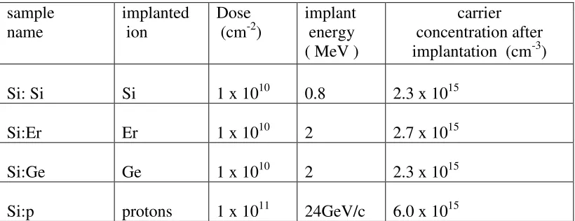
to an anneal, and whether they exhibit electrical activity. Figure 1 shows the DLTS
spectra of Si implanted with protons, Si and Er. The spectrum from the Si implanted
with Ge was virtually identical to the Er-implanted one, and is not shown for clarity.
It is clear that the ratio of the peak height at approximately 235K to the peak height at
100K is changing. The lighter particles produce a ratio between the two peak heights
below 5, whereas the heavier, rare earth ions produce a value two orders of magnitude
greater than this. Inspection shows that this peak also changes to a lower temperature
by about 10K in the case of the rare earth implant. Because of these differences, we
deduce that the overall effect of an ion implant is primarily apparent in the feature at
around 235K.
Because of the existence of the vacancy-rich and interstitial-rich regions in implanted
silicon, it is important to establish whether the two regions have different electrical
signatures in DLTS or LDLTS before continuing to investigate the end of range
region. Comparison of Capacitance-Voltage (C-V) data with simulations of the
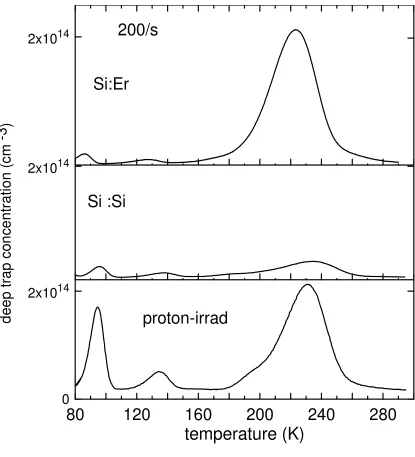
implant profile by TRIM determined that a reverse bias of –2 V and fill pulse of –1 V
would examine the vacancy-rich region, and a reverse bias of –5 V and fill pulse of –4
V would examine the interstitial-rich region of the implanted samples. The DLTS
profiles look identical, but, as has been explained previously, broad DLTS peaks may
often contain much extra detail about closely spaced deep levels. Figure 2 shows the
LDLTS of the low dose Er-implanted Si, before annealing. The measurement
temperature was 225K. The LDLTS spectra of the vacancy-rich and interstitial-rich
in proton-irradiated silicon. If protons are implanted, one sees either one or two lines
in the LDLTS spectrum at 225K depending upon the doping, due to the singly
charged divacancy, VV, and the dopant-vacancy pair, (VP in this case), if the
background doping is high enough [7]. Figure 2 shows more than two components in
the capacitance transient in both cases: three from the interstitial-rich region and five
from the vacancy-rich region. All ion implanted samples in this study showed the
same trend of five emission rates in the vacancy-rich region, simplifying to three in
the interstitial-rich region. Repeated experiments over several days showed that the
results were reproducible, and all emission rates increased with temperature, as should
be the case for emission from deep states. However, because the capacitance transient
displayed so many components, the trap concentration of each individual deep level
was small. Therefore, the signal to noise ratio was quite low, and Arrhenius plots to
obtain the activation energies were not possible. The proton-irradiated silicon sample
did not exhibit a complex structure in the LDLTS spectra recorded at this temperature.
We therefore deduce that this is the peak in the DLTS spectrum which contains the
most information about defects in ion implanted Si, and, furthermore, it contains
emission from traps present in the vacancy- and interstitial-rich regions.
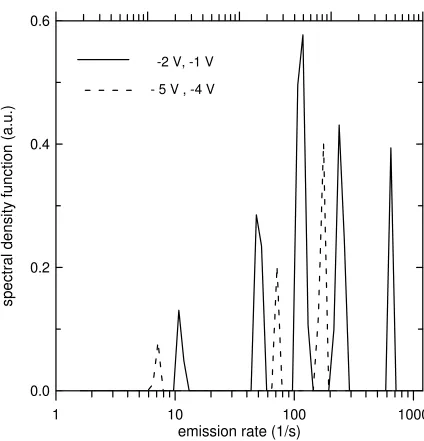
In order to determine if the interstitial-rich region contains defects that are larger than
isolated point defects, the DLTS peak at 225K was measured by DLTS at a reverse
voltage of -5V and a fill voltage of -4V, to exclude the vacancy-rich region. The fill
pulse duration was varied and the data plotted in accordance with equation 1. Figure
3 shows the results of this exercise for the Er-implanted Si, and it can be seen that the
data do not lie on a straight line. However, the data for the proton-irradiated Si lie on a
sample are dominated by larger defects which exhibit a time-dependent capture
cross-section: i.e. they charge up as they fill with carriers and become progressively more
repulsive to further carrier capture.
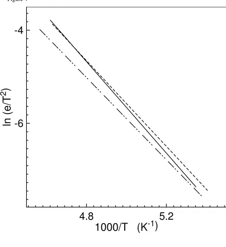
Figure 4 shows the Arrhenius plots for the stacking faulted sample at three different
fill pulse lengths, for a large DLTS peak centred at 250K (not shown). A fill pulse of
0.1ms yields an activation energy of Ec – 420meV, a fill pulse of 1ms yields an
activation energy of Ec – 395meV and a fill pulse of 5ms yields an activation energy
of Ec – 350meV. Therefore as the fill pulse increases, the apparent depth of the deep
level below the conduction band decreases. This can be explained as follows. At the
core of the dislocation the conduction band edge is disturbed and rises, increasing the
distance between it and the trap level [11]. As deep levels at the dislocation fill, the
dislocation core charges up and becomes less attractive to carriers. As time goes by,
deep levels that are physically further away from the core fill up, and at these points,
in real space, the trap level is nearer to EC. This modification of the band structure due
to dislocations has recently been utilised to obtain light from Si by using local carrier
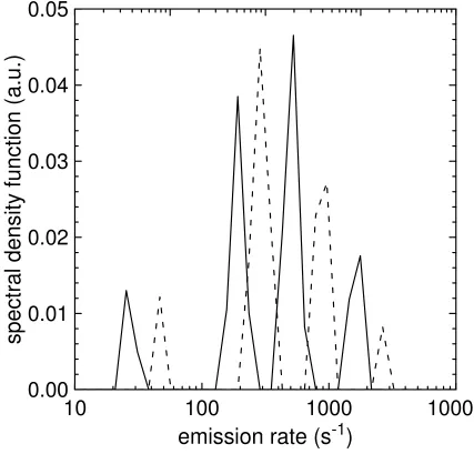
trapping [19]. The stacking faults also exhibit multiple LDLTS lines which change
their emission rate with fill pulse length, as shown in Figure 5. The combination of
these two results suggests that the dislocations bounding the stacking faults also have
a time-dependent capture cross-section, as has been reported previously [12] .
Application to device development
In the future, tighter size tolerances for smaller dimensions in electronic devices will
mean that defect control and defect engineering will continue to be major issues in the
Silicon still dominates the electronics market, itself worth hundreds of billion dollars
per year. The dimensions of deep sub-micron silicon-related devices have now shrunk
to nano-scale lengths, e.g. a 20nm base width in a SiGe HBT or the <65nm gate
length in a MOSFET, i.e. just hundreds of atomic spacings. Such devices require
complete understanding and control of effects such as the clustering of impurities or
intrinsic defects, defects in novel, compound or strained substrates, vacancy and/or
interstitial enhanced diffusion, and the causes of leakage in very highly doped
junctions. Si channels in MOSFETS are now often produced with compressive strain
by selectively growing doped source/drain (S/D) regions by CVD. These S/D regions
are not currently implanted in a commercial process because there is no
comprehensive information yet available on the implantation damage introduced into
IV-IV compounds. P-well doping is commonly used in transistors before the highly
doped, shallow source and drain regions are implanted, but there will be end-of-range
damage which extends into the p-well and this is not fully understood. Transient
Enhanced Diffusion (and thermal diffusion) of B in Si can be suppressed by F
implantation, which may form larger defects that soak up interstitials [6] . However
the detailed electrical activity of F clusters (with anything) is yet to be established.
These topics can now be tackled by a combination of DLTS and LDLTS, based upon
the results from the simpler ion-implanted systems reviewed in this paper.
Conclusions
Samples containing ion implant damage, caused by a variety of ion species, have been
characterised by DLTS and high resolution LDLTS. Oxidation induced stacking
sample. In all cases the conventional DLTS showed broad peaks but the LDLTS
showed a rich structure of either three or four components in the capacitance transient.
Capture cross section measurements on the predominant defect in the end-of-range
region in the ion implanted samples show that the end of range defects do not have
point-defect-like properties. They have capture behaviour typically associated with
larger (more than one atom) defects, and the capacitance change is linearly dependent
upon the logarithm of the fill pulse length. It has also been possible, using LDLTS, to
observe the same effect in the stacking fault control sample,,i.e. the boundary
dislocations of the stacking faults exhibit emission rates which are dependent upon
the fill pulse length. The electrical behaviour of the defects in the end-of-range region
of ion-implanted samples has therefore been shown to be the same as that of much
longer extended defects. This paves the way for studies of problems arising from
multiple implants typically carried out in silicon processing for electronic devices at
or near the ITRS timeline.
Acknowledgements
We should like to acknowledge Surrey University in the UK for the ion implantations.
Part of this work was funded by the United Kingdom Engineering and Physical
Sciences Research Council (EPSRC). KVP acknowledges the support of EPSRC
References
[1] G. Mannino, N. E. B. Cowern, F. Roozeboom, and J. G. M. van Berkum, Appl. Phys. Lett., 76 (2000) 855.
[2] S. Libertino, S. Coffa S, and J. L. Benton, Phys. Rev. B, 63 (2001) 195206
[3] B.G. Svensson, C. Jagadish, A. Hallen, and J. Lalita, Phys. Rev. B, 55 (1997) 10498
[4] P. Pellegrino, N. Keskitalo, A. Hallen, and B. G. Svensson, Nucl. Instr. Meth. B, 148 (1999) 306
[5] N. Abdelgader and J. H. Evans-Freeman, J. Appl. Phys., 93 (2003) 5118
[6] H A W El Mubarek, J M Bonar, G D Dilliway, P Ashburn, M Karunaratne, A F Willoughby, Y Wang, P L F Hemment, R Price, J Zhang and P Ward, J Appl Phys 96 (2004) 4114
[7] G.D. Watkins and J.W. Corbett, Phys. Rev. 138 (1965) A543
[8] M.T Asom, J.L. Benton, R. Sauer and L.C. Kimerling, Appl. Phys. Lett. 51 (1987) 256
[9] J. Lalita , B.G. Svensson, C. Jagadish and A. Hallen, Nucl. Instr. and Meth. B 127/128 (1997) 69
[10] J.H. Evans-Freeman, P.Y.Y. Kan and N. Abdulgader, J. Appl. Phys. 92 (2002) 3755
[11] P.R. Wilshaw and G.R. Booker, Proceedings of the Microscopical Society Conference, (1985) 329
[12] Y.Qian, J.H.Evans and A.R.Peaker, Inst. Phys. Conf. Ser. No. 134 (1993) 121
[13] L. Dobaczewski, P. Kaczor, I. Hawkins, and A. R. Peaker, J. Appl. Phys.76 (1994) 194
[14] J. F. Ziegler, J. P. Biersack and U. Littmark, "The Stopping and Range of Ions in Solids" Pergamon, New York, 1985; http://www.srim.org/
[15] A. Ourmazd, P. R. Wilshaw and G. R. Booker, Physica B 116, 600 (1983)
[16] K. H. Yang, J. Electrochem. Soc. 131, 1140 (1984)
[18] P. Pellegrino, P. Leveque, J. Wong-Leung, C. Jagadish and B. G. Svensson, Appl. Phys. Lett. 78, 3442 (2001)
Table 1 Samples used in this work
sample name
implanted ion
Dose (cm-2)
implant energy ( MeV )
carrier concentration after implantation (cm-3)
Si: Si Si 1 x 10¹⁰ 0.8 2.3 x 10¹⁵
Si:Er Er 1 x 10¹⁰ 2 2.7 x 10¹⁵
Si:Ge Ge 1 x 10¹⁰ 2 2.3 x 10¹⁵
Figure Captions
Figure 1 DLTS of Er-and Si-implanted Si, and proton-irradiated Si.
Figure 2 LDLTS of low dose Er-implanted Si, before annealing. The measurement
temperature was 225K and the experiments were carried out at two voltage ranges: a
reverse bias of –2 V and fill pulse of –1 V which samples the vacancy-rich region, and
a reverse bias of –5 V and fill pulse of –4 V which samples the interstitial-rich region.
Figure 3 The capacitance transient height plotted as a function of DLTS fill pulse
duration, in accordance with equation 3, for Si:p, irradiated with protons ( ) and low
dose Er-implanted Si, (+).
Figure 4 Arrhenius plots of Si containing stacking faults at fill pulses 0.1ms ( ___ )
with Ea = 420meV, 1ms ( _ _ _ ) with Ea = 395meV and 5ms (____ _ _ ) with Ea =
350meV.
Figure 1
80
120
160
200
240
280
Figure 2
1
10
100
1000
emission rate (1/s)
0.0
0.2
0.4
0.6
s
p
e
c
tr
a
l
d
e
n
s
it
y
f
u
n
c
ti
o
n
(
a
.u
.)
-2 V, -1 V
Figure 3
0
100
200
pulse length ( s)
-3.0
-2.0
-1.0
ln
[(
C
m
a
x
-C
t)
/C
m
a
x
]
Figure 4
4.8
5.2
1000/T (K
-1
)
-6
-4
ln
(
e
/T
Figure 5
10
100
1000
10000
emission rate (s
-1
)
0.00
0.01
0.02
0.03
0.04
0.05
s
p
e
c
tr
a
l
d
e
n
s
it
y
f
u
n
c
ti
o
n
(
a
.u