Atomic-‐scale Electronic Structure of the Cuprate
d
-‐Symmetry Form Factor Density Wave State
M. H. Hamidian1†, S.D. Edkins1,2†, Chung Koo Kim3, J. C. Davis1,2,3,4, A. P. Mackenzie2,5, H. Eisaki6, S. Uchida7, M. J. Lawler1,8, E.-‐A. Kim1, S. Sachdev9,10, and K. Fujita3
1. LASSP, Department of Physics, Cornell University, Ithaca, NY 14853, USA.
2. School of Physics and Astronomy, University of St. Andrews, Fife KY16 9SS, Scotland. 3. CMPMS Department, Brookhaven National Laboratory, Upton, NY 11973, USA.
4. Kavli Institute at Cornell for Nanoscale Science, Cornell University, Ithaca, NY 14853, USA. 5. Max-‐Planck Institute for Chemical Physics of Solids, D-‐01187 Dresden, Germany.
6. Institute of Advanced Industrial Science and Technology, Tsukuba, Ibaraki 305-‐8568, Japan. 7. Department of Physics, University of Tokyo, Bunkyo-‐ku, Tokyo 113-‐0033, Japan.
8. Dept. of Physics and Astronomy, Binghamton University, Binghamton, NY 13902.
9. Department of Physics, Harvard University, Cambridge, MA.
10. Perimeter Institute for Theoretical Physics, Waterloo, Ontario N2L 2Y5, Canada † These authors contributed equally to this project.
ABSTRACT
phase π compared to those at E=Δ1 (empty states). Finally, we show that the dFF-‐DW Q corresponds directly to scattering between the ‘hot frontier’ regions of k-‐space beyond which Bogoliubov quasiparticles cease to exist31,32,33. These data demonstrate that the dFF-‐DW state is consistent with particle-‐hole interactions focused at the pseudogap energy scale and between the four pairs of ‘hot frontier’ regions in k-‐space where the pseudogap opens.
A conventional ‘Peierls’ charge density wave (CDW) in a metal results from
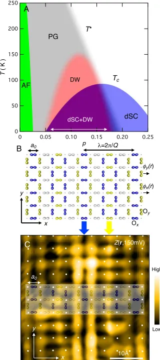
particle-‐hole interactions which open an energy gap at specific regions of k-‐space that are connected by a common wavevector Q. This generates a modulation in the density of free charge at Q along with an associated modulation of the crystal lattice parameters. Such CDW states are now very well known34. In principle, a density wave modulating at Q can also exhibit a ‘form factor’ (FF) with different possible symmetries35,36(see Supplementary Information (SI) Section 1). This is relevant to the high-‐temperature superconducting cuprates because numerous researchers have recently proposed that the ‘pseudogap’ regime1,2 (PG in Fig. 1A) contains an unconventional density wave with a d-‐symmetry form factor18-‐30. The basic phenomenology of such a state is that intra-‐unit-‐ cell (IUC) symmetry breaking renders the Ox and Oy sites within each CuO2 unit-‐cell electronically inequivalent, and that this inequivalence is then modulated periodically at wavevector Q parallel to (1,0);(0,1). The real-‐space (r-‐space) schematic of such a d-‐ symmetry FF density wave (dFF-‐DW) at 𝑸𝒙 as shown in Fig. 1B exemplifies periodic
it is essential to establish its atomic-‐scale phenomenology, including the k-‐space eigenstates contributing to its spectral weight, the relationship (if any) between modulations occurring above and below the Fermi energy, whether the modulating states in the DW are associated with a characteristic energy gap, and how the dFF-‐DW evolves with doping.
To visualize such phenomena directly as in Fig. 1C, we use sublattice phase-‐
resolved imaging of the electronic structure14 of the CuO2 plane. Both the scanning tunneling microscope (STM) tip-‐sample differential tunneling conductance !"
!"(𝒓,𝐸 = 𝑒𝑉) ≡𝑔(𝒓,𝐸) and the tunnel-‐current 𝐼 𝒓,𝐸 are measured at bias voltage V=E/e and with sub-‐unit-‐cell spatial resolution. Because the density-‐of-‐electronic-‐states 𝑁(𝒓,𝐸) is related to the differential conductance as 𝑔 𝒓,𝐸 ∝ 𝑒𝐼!/ !"!𝑁(𝒓,𝐸′)𝑑𝐸′
! 𝑁(𝒓,𝐸) with Is
and Vs being arbitrary parameters and the denominator !"!𝑁(𝒓,𝐸′)𝑑𝐸′
! unknown, valid
determination of 𝑁(𝒓,𝐸) is impossible (SI Section 2). However, one can suppress these serious systematic errors by using 𝑅 𝒓,𝐸 = 𝐼(𝒓,𝐸)/𝐼 𝒓,−𝐸 or 𝑍 𝒓,𝐸 = 𝑔(𝒓,𝐸)/ 𝑔 𝒓,−𝐸 ; this allows distances, wavelengths, and spatial-‐phases of electronic structure to be measured accurately. The unprocessed 𝑔(𝒓,𝐸) acquired for and analyzed in this paper: (i) are measured over very large fields of view (to achieve high phase-‐precision in Fourier analysis) ; (ii) simultaneously maintain deeply sub-‐unit-‐cell precision measurements in r (to achieve high precision in sublattice segregation); (iii) are taken over a wide range of energies E with fine energy-‐spacing, so that energy dependences of d-‐symmetry FF modulations may be accurately determined. We then calculate each sublattice-‐phase-‐resolved 𝑍 𝒓,𝐸 image and separate it into three: the first, Cu(r), contains only the measured values of Z(r) at Cu sites while the other two, Ox(r) and Oy(r), contain only the measurements at the x/y-‐axis oxygen sites. Phase-‐resolved Fourier
𝑂! 𝒒 = 𝑅𝑒𝑂! 𝒒 +𝑖𝐼𝑚𝑂! 𝒒 ; 𝑂! 𝒒 = 𝑅𝑒𝑂! 𝒒 +𝑖𝐼𝑚𝑂! 𝒒 , are used to determine the form factor symmetry for modulations at any q
𝐷! 𝒒 = (𝑂
! 𝒒 −𝑂! 𝒒 )/2 (1a)
𝑆′! 𝒒 =( 𝑂
! 𝒒 +𝑂! 𝒒 )/2 (1b)
𝑆! 𝒒 =𝐶𝑢 𝒒 (1c)
where the superscript Z identifies the type of sublattice resolved data used. Specifically for a DW occurring at Q, one can then evaluate the magnitude of its d-‐symmetry form factor 𝐷 𝑸 and its s’-‐ and s-‐symmetry form factors 𝑆′ 𝑸 and 𝑆 𝑸 , respectively. Studies of non-‐energy-‐resolved 𝑅 𝒓,𝐸 images using this approach have revealed that the DW modulations in the Ox(r) and Oy(r) sublattice images of electronic structure in underdoped Bi2Sr2CaCu2O8+x and Ca2-‐xNaxCuO2Cl2 consistently exhibit a relative phase of πand therefore a d-‐symmetry form factor14; X-‐ray scattering studies15,16 yield the same conclusion for two other cuprates, YBa2Cu3O7-‐x and Bi2Sr2-‐xLaxCuO6+δ.
X-‐ray scattering studies report a short-‐ranged density wave with wavevector
fashion yields 2C,D; both clearly exhibit the dFF-‐DW maxima at the two inequivalent wavevectors 𝑸! and 𝑸!. Fourier filtering these two 𝐷! 𝒒 from 2A,B for only those regions surrounding 𝑸! and 𝑸! (within dashed circles) generates two complex-‐valued images 𝐷! 𝒓 ,𝐷! 𝒓
𝐷! 𝒓 = 22𝜋2 𝑑𝒒𝑒𝑖𝒒∙𝒓𝐷𝑍(𝒒)𝑒−𝒒−𝑸𝑥
2
2Λ2 ; 𝐷! 𝒓 = 2
2𝜋 2 𝑑𝒒𝑒𝑖𝒒∙𝒓𝐷
𝑍 (𝒒)𝑒−
𝒒−𝑸𝑦2
2Λ2 (2a)
where Λ-‐1 is the characteristic length scale over which variations in 𝐷! 𝒓 ,𝐷! 𝒓 can be resolved, set by the filter width in Fourier space.
Their magnitudes
|𝐷! 𝒓 |= 𝑅𝑒𝐷! 𝒓 !+ 𝐼𝑚𝐷! 𝒓 ! (2b)
|𝐷! 𝒓 |= 𝑅𝑒𝐷! 𝒓
!
+ 𝐼𝑚𝐷! 𝒓 !
(2c)
represent the local amplitudes of dFF-‐DW modulations along 𝑸! and 𝑸!, respectively. Any unidirectional domain arrangements of the dFF-‐DW state can then be determined by introducing
𝐹
𝒓
=
|!! 𝒓 |!|!! 𝒓 ||!! 𝒓 |!|!! 𝒓 |
(3)
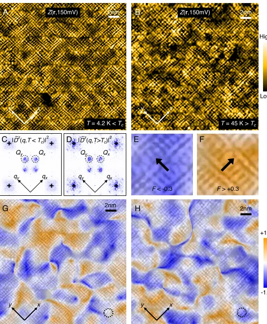
These observations of coexisting nanoscale unidirectional regions are in reasonable agreement with related X-‐ray studies37 of YBa2Cu3O7-‐x. Finally, since the data in Fig. 2B and Fig. 2H were measured at T>Tc (pink region Fig. 1A), it demonstrates directly that the cuprate dFF-‐DW appears first in the non-‐superconducting ‘pseudogap’ regime.
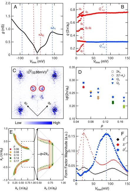
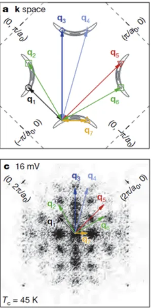
A conventional CDW state opens a gap in the energy spectrum of k-‐space
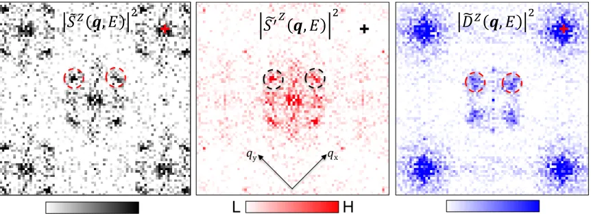
electronic eigenstates with the maximum spectral weight of modulating states occurring at the edges of this energy-‐gap34. But which energy gap (if any) is associated with the dFF-‐DW state found in underdoped cuprates is unknown. Figure 3A shows how a typical tunneling conductance spectrum representative of strongly underdoped cuprates exhibits two characteristic energies 31,32,33. While the lower energy scale Δ0 represent the maximum energy at which Bogoliubov quasiparticle excitations exist31,32,33 (see Figure 3B) the higher energy scale (dashed blue line) is the cuprate ‘pseudogap’ as determined from its comparison with doping dependence of pseudogap scale in tunneling and photoemission. To identify the energy dependence of the cuprate dFF-‐DW states, we measure 𝑍 𝒓, 𝐸 and from it calculate 𝐷! 𝒒, 𝐸 , 𝑆′! 𝒒, 𝐸 , and 𝑆! 𝒒, 𝐸 . Figure 3C shows the measured power-‐spectral-‐density of the d-‐symmetry FF modulations
𝐷! 𝒒, 88meV !, with the wavevectors near 𝑸
! and 𝑸! indicated by red circles.
dependence of the dFF-‐DW wavevectors (blue line) determined in this way for a p = 0.06 sample. Such information was not previously available from measurements of the modulation wavevectors from STM images lacking sublattice phase-‐resolved segregation14 into 𝑂
! 𝒒 and 𝑂! 𝒒 . Figure 3E shows the measured k-‐space locus where
Bogoliubov quasiparticles exist31,32,33 as a function of hole density. When the dispersive ‘octet’ of Bogoliubov scattering interference disappears a transition occurs to a non-‐ dispersive density wave modulation (Fig. 3B). In Fig. 3D, the doping dependence of the conventional Qx, Qy of the d-‐symmetry form factor modulations is shown using blue symbols, while the measured shortest wavevectors interconnecting the k-‐space arc tips (Fig. 3E) are indicated by using colored symbols referring to each hole-‐density in Fig. 3E. These data demonstrate directly that the conventional Qx, Qy of the dFF-‐DW state corresponds to the locations in k-‐space of arc tips. Finally, in Fig. 3F we show the measured energy dependences of the amplitudes of the s, s’-‐ and d-‐form factor modulations, SZ(E), S’Z (E) and DZ (E), determined by integrating over the region of q-‐ space enclosed by solid red circles in 3C (SI Section 5). The d-‐symmetry form factor is negligible for modulations in the low energy range that contains only Bogoliubov quasiparticles (and which we now see is dominated by s’-‐symmetry form factors) but it rapidly becomes intense at higher energy and reaches maximum at the pseudogap energy scale which for this sample is Δ1~90meV. This reveals that the characteristic energy of electronic-‐structure modulations in the cuprate d-‐symmetry FF density wave is actually the pseudogap energy.
As a function of energy, the transition from Bogoliubov quasiparticle
interference modulations to dFF density wave modulations occurs in an unusual fashion.
are observed31,32,33. Here, the set of seven dispersive scattering interference modulations q1,q2,…q7 signifying Bogoliubons32 (SI Section 5) disappears in a narrow energy window during which dispersion of the two surviving modulations q1(E) and q5(E) comes to a halt, leaving the non-‐dispersive dFF-‐DW modulations with q1* ≈ q1(Δ0) and q5*≈ q5(Δ0)
(see Fig. 3B and Refs. 31,32,33). The intensity of these modulations first becomes
detectable at Δ0 and, as we show below, reaches an intense maximum at Δ1, all the while
maintaining the same wavevectors Qxd and Qyd as shown in Fig. 3B. We refer to this k-‐ space region where Bogoliubov quasiparticles yield to modulations of a dFF-‐DW as the
‘hot frontier’39 to distinguish it from the colloquial ‘hot spots’ beyond which, in a
conventional density wave, dispersive quasiparticle states would reappear. In cuprates,
this does not occur and, instead, the ‘hot frontiers’ define the k-‐space limit beyond which
only dFF-‐DW modulations are detected31,32,33 using SI-‐STM (blue in Fig. 3B).
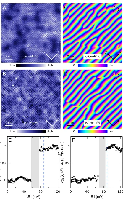
Key information on the microscopic cause of any DW state is also contained in
the relationship between modulations of states above and below the Fermi energy. For example, mixing via interactions of states with momenta 𝒌𝟏and 𝒌𝟐 generates modulations at wavevector 𝑸=𝒌𝟏−𝒌𝟐 . The wavefunctions of any resulting DW would
then form bonding/anti-‐bonding states below/above the Fermi level which are
proportional to 𝑒!𝒌!∙𝒓±𝑒!𝒌!∙𝒓
.
The related densities of these states would then exhibitmodulations governed by 𝑒!𝒌!∙𝒓±𝑒!𝒌!∙𝒓 !=2(1±𝐶𝑜𝑠 𝑸∙𝒓 ). In such scenarios, the DW
modulations above the Fermi energy should always beπ out-‐of-‐phase with the
equivalent ones below. To explore this issue in Bi2Sr2CaCu2O8+x, we show in Figs 4A,B the
measured g(r, +94meV) from filled states and g(r,-‐94meV) from empty states, respectively, each at the characteristic energy of the dFF-‐DW (Fig 3F and SI Section 6). For these two images the sublattice-‐phase-‐resolved 𝐷! 𝒒,𝐸 (Eqn. 1a) are calculated
𝑸! and 𝑸! in Figs 4A,B. Next, by Fourier filtering these two 𝐷! 𝒒,𝐸 for regions surrounding 𝑸! we determine the complex-valued 𝐷! 𝒓 and thus the spatial phase of dFF-‐DW
modulation along 𝑸! as
𝜙! 𝒓,𝐸 =arctan 𝐼𝑚𝐷! 𝒓,𝐸 /𝑅𝑒𝐷! 𝒓,𝐸 (4a)
For E=+94meV this is shown in Fig. 4C and for E=-‐94meV in Fig. 4D. Visual comparison reveals that these two 𝜙! 𝒓,±𝐸 images are out of phase with each other by π. And indeed, the spatial-‐average value of 𝜙! 𝒓,+𝐸 −𝜙! 𝒓,−𝐸 as a function of E (over the whole field of view A and B) is shown in Fig. 4F. It reveals that, while the relevant 𝑸! and 𝑸! components of g(r,+E) and g(r,-‐E) images are in phase with each other at low energy, they rapidly evolve at |E|>70meV and become globally π out of phase at |E|~Δ1 (Figs 4A,B). The shaded region indicates evolution through a situation where some areas exhibit 𝜙 ~0 and some 𝜙 ~π but this is quickly resolved upon reaching pseudogap energy Δ1. Similar analysis for the particle-‐hole symmetry in phases 𝜙! 𝒓,±𝐸 of
𝑸! modulations
𝜙! 𝒓,𝐸 = arctan 𝐼𝑚𝐷! 𝒓,𝐸 /𝑅𝑒𝐷! 𝒓,𝐸 (4b)
yields a virtually identical result. These phenomena also occur throughout the underdoped regions the phase diagram (SI Section 6.III). All these data demonstrate that a phase difference of π exists between spatial modulations of the filled states at pseudogap energy E~-‐Δ1 and the empty states at E~+Δ 1 , for the cuprate dFF-‐DW state.
To summarize: by introducing new techniques to determine the
2G,H). The conventionally defined wavevectors Qx and Qy of the dFF-‐DW state evolve with doping as determined by the four shortest scattering vectors linking the k-‐space regions beyond which Bogoliubov quasiparticle excitations are nonexistent (Figs 3D,E) and at which the pseudogap emerges. Further, we demonstrate that, as determined in terms of tunneling probabilities, the dFF-‐DW state is particle–hole antisymmetric in the sense that a phase difference of π exists between spatial modulations of the filled states (E~-‐Δ1) and the empty states ( E~+Δ 1 ) (Fig. 4E). Most significantly, we show that the characteristic energy of the dFF-‐DW electronic-‐structure modulation is actually the pseudogap energy Δ1 (Fig. 3F).
These data provide evidence that the cuprate d-‐symmetry form factor density
support a microscopic picture in which the exotic electronic structure of the pseudogap is parent to the dFF-‐DW state and not vice-‐versa, where the energy-‐scale and wavevectors of the dFF-‐DW are intimately linked to those of the pseudogap, and in which the dFF-‐DW competes directly for spectral weight with the d-‐symmetry superconductor at the k-‐space ‘hot frontier’ between superconductivity and the
Figure Captions
Figure 1 d-symmetry form factor density wave in cuprate pseudogap phase.
A. Schematic phase diagram of hole-doped cuprates. The pseudogap regime has been identified by, for example, suppression of uniform magnetic susceptibility and electronic specific heat, and the appearance of a truncated Fermi surface referred to as the ‘Fermi Arc’ 1,2. The dome-shaped region of d-symmetry Cooper paired high temperature superconductivity is universally accepted. More recently, an unusual density wave state has been detected by bulk probes4-13 in the region indicated schematically in pink; its modulations are now known to have a d-symmetry form factor 14-17. The range of hole-density, p, in which d-symmetry form factor density
waves are studied in this paper is indicated by the white double-headed arrow.
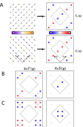
B. Schematic of the electronic structure in a cuprate dFF-DW. Grey dots represent the Cu sites and correspond to the white dots in 1C. The Ox and Oy sites within each CuO2 unit-cell are electronically inequivalent as represented by a color scale ranging
from yellow through white to blue. The schematic DW modulates horizontally with wavelength λ or with wavevector Qx (horizontally) and with period 4a0. The periodic
modulations at Ox sites are πout of phase with those at Oy sites as seen by
considering the two trajectories marked φx and φy (SI Section 1).
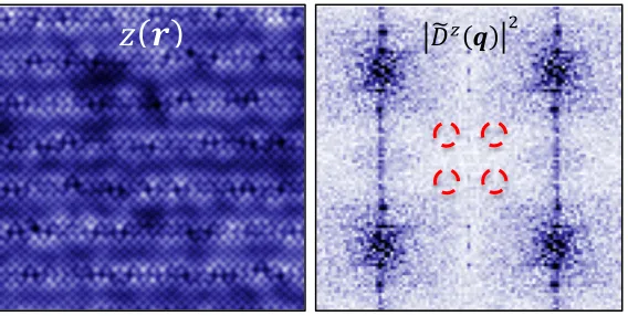
C. Measured Z(r,150meV) at T>Tc in the pseudogap phase of Bi2Sr2CaCu2O8 at
hole-density p~8%. Two periods of dFF-DW modulation at Qx that correspond directly to
the schematic in 1B are shown. Thus, to observe the dFF-DW state sublattice-phase-resolved imaging is required and achieved here in the pseudogap regime. The transparent overlay shows the relationship between locations of Cu, Ox, Oy atoms in
Figure 2 dFF-DW domains in superconducting and pseudogap phases.
A. Measured Z(r,150meV) at T<<Tc in the superconducting phase of hole density p~8%
doped Bi2Sr2CaCu2O8+x (T~4.2K). These complex spatial features involve modulations that comprehensively maintain a relative phase of π between Ox and Oy
in a disordered d-symmetry FF density wave.
B. Measured Z(r,150meV) at T>Tc in the pseudogap phase of hole density p~8% doped
Bi2Sr2CaCu2O8 (T~45K). Although correlation lengths are shorter, the dFF-DW
phenomena are otherwise indistinguishable from observations at T<<Tc.
C. The d-symmetry form factor power spectral density 𝐷!(𝒒) !=| 𝑂
! 𝒒 −𝑂! 𝒒 /2|2
determined from sublattice-phase resolved analysis of data in A. Two primary DW peaks at Qx and Qy exist with this d-symmetry form factor, as identified by dashed
circles.
D. The d-symmetry FF power spectral density 𝐷!(𝒒) ! =| 𝑂
! 𝒒 −𝑂! 𝒒 /2 |2
determined from sublattice-phase resolved analysis of data in B. Again, two primary DW peaks at Qx and Qy exist with this d-symmetry form factor, showing that the q
-space structure of dFF-DW phenomenology is identical in the pseudogap phase and in the superconducting phase.
E. F. Using only the regions within the dashed circles in C,D, the r-space amplitudes of the dFF-DW in A,B are calculated for modulations along Qx from Eqn. 2a, and along
Qy from Eqn. 2b. Then using 𝐹 𝒓 =(|𝐷! 𝒓 |−|𝐷! 𝒓 |)/(|𝐷! 𝒓 +|𝐷! 𝒓 |) (see SI
Section 3) regions primarily modulating along y-axis with -1.0< 𝐹 𝒓 <-0.3 are shaded blue.Regions primarily modulating along x-axis with +0.3< 𝐹 𝒓 <+1.0 are shaded orange
F. Domain configuration of unidirectional dFF-DW modulations contained in Fig. 1A at
T<<Tc. The unidirectionality color scale for 𝐹 𝒓 demonstrated in E,F is overlaid upon
G. Domain configuration of unidirectional dFF-DW modulations contained in Fig. 1B at
T>Tc. The unidirectionality color scale for 𝐹 𝒓 demonstrated in E,F is overlaid upon
the data in B. The dashed circle has same definition as in G.
Figure 3 Concentration of dFF-DW Spectral Weight on Pseudogap Energy
A. The tunneling density of states spectrum g(E=eV)=dI/dV(E) typical of underdoped cuprates show for the p~8% samples presented in this paper. The energy Δ0 beyond
which Bogoliubov QPI do not exist3233 and the pseudogap energy Δ1 are indicated.
B. The energy dispersion of seven dispersive modulation characteristic of Bogoliubov quasiparticle excitations of a d-wave superconductor (q1…q7). These Bogoliubov
quasiparticle interference modulations are all simultaneously observable only below the energy ∆0as indicated by dashed red line (Refs.31, 32, 33); here we demonstrate
that they exhibit a predominantly s’-symmetry form factor indicated by the red color. At energies above ∆0, the electronic structure images evolve quickly to consist of only
non-dispersive Qxd and Qyd wavevectors of the d-symmetry form factor DW. We plot
the dispersion of these modulations as the energy dependence of the maxima in
𝐷 𝒒,𝐸 using blue squares. The same physical modulations when analyzed using
𝑆′ 𝒒,𝐸 appear as the non-dispersive Qxs’ and Qys’ wavevectors shown as red circles.
C. Measured 𝐷!(𝒒,88 meV) !for samples studied herein. The Q
xd and Qyd wavevectors
of the d-symmetry form factor DW are indicated by two red circles; the data of relevance for determining energy/momentum dependence of the dFF DW modulations is contained within.
D. Measured doping dependence of Qx and Qy of d-symmetry form factor DW in
underdoped Bi2Sr2CaCu2O8+x.is shown using blue symbols. The measured doping
E. Measured doping dependence of the wavevectors interconnecting the k-space arc tips at which Bogoliubov quasiparticle signatures disappear (B & Refs.31,32,33).
F. Measured energy dependence of S’(E) where q is integrated over the region inside
solid red circles in C, is shown in red. Measured energy dependence of S(E) where q is integrated over the region inside solid red circles in C, is shown in black. Measured energy dependence of d-symmetry form factor D(E) where q is integrated over the region inside solid red circles in C is shown in blue (SI Section 4). These data reveal that the dFF-DW spectral weight is concentrated at energy surrounding ~90meV which, at this hole density, is the independently measured pseudogap energy scale Δ1 (see Fig. 3A) and indicated on all relevant panels by a dashed blue
line.
Figure 4 Relationship betweendFF-DW modulations of filled andempty states
A. Differential tunneling conductance image g(r,+94meV) measured above EF near the
pseudogap energy +Δ1. The color scale is reversed compared to B.
B. Differential tunneling conductance image g(r,-94meV) measured below EF near the
pseudogap energy -Δ1. The color scale is reversed compared to A.
C. The spatial phase of the dFF-DW modulating along the y-direction 𝜙! 𝒓,𝐸 is
calculated using Eqn. 4a from g(r,+94meV) data in A. The dashed circle shows the r -space radius equivalent to the q-space filter used to generate the 𝜙!,! 𝒓,𝐸 images
by Fourier filtering (see SI Section 6).
D. The spatial phase of the dFF-DW modulating along the y-direction 𝜙! 𝒓,𝐸 is
calculated using Eqn. 4b from g(r,-94meV) data in B.
E. & F. From the FOV of A and B, we show the energy dependence of the relative phase of g(r,-E) and g(r,+E) modulations along the y-axis (SI Section 5): 𝜙! 𝒓,+𝐸 −
relative phase of g(r,-E) and g(r,+E) for modulations along the x-axis: 𝜙! 𝒓,+𝐸 −
𝜙! 𝒓,−𝐸 .The low energy E<Δ0 Bogoliubov quasiparticle modulations at +E and -E
are in phase spatially and so have relative phase difference of 0. As the pseudogap energy Δ1 is approached and the dFF-DW phenomena emerge, the relative spatial
phase of empty-state an filled state dFF-DW modulations varies wildly in the narrow energy grange shaded gray, and the quickly develops a robust phase shift of π.
Acknowledgements
We acknowledge and thank H. Alloul, D. Chowdhury, R. Comin, A. Damascelli, E. Fradkin, D. Hawthorn, J. E. Hoffman, M.-‐H. Julien, D. H. Lee, M. Norman, and C. Pepin for helpful discussions and communications. We are especially grateful to S.A. Kivelson for key scientific discussions and advice. Experimental studies were supported by the Center for Emergent Superconductivity, an Energy Frontier Research Center, headquartered at Brookhaven National Laboratory and funded by the U.S. Department of Energy under DE-‐2009-‐BNL-‐PM015, as well as by a Grant-‐in-‐Aid for Scientific Research from the Ministry of Science and Education (Japan) and the Global Centers of Excellence Program for Japan Society for the Promotion of Science. CKK acknowledges support under FlucTeam program at Brookhaven National Laboratory Contract DE-‐AC02-‐98CH10886. S.D.E., J.C.D. and A.P.M acknowledge the support of EPSRC through the Programme Grant ‘Topological Protection and Non-‐Equilibrium States in Correlated Electron Systems”. Theoretical studies at Cornell University were supported by NSF Grant DMR-‐0955822. Theoretical studies at Harvard University were supported by NSF Grant DMR-‐1103860 and by the Templeton Foundation. Research at Perimeter Institute is supported by the Government of Canada through Industry Canada and by the Province of Ontario through the Ministry of Research and Innovation.
References
1 Orenstein J, Millis AJ (2000) Advances in the physics of high-‐temperature superconductivity. Science 288(5465):468―474.
2 M. R. Norman, D. Pines, and C. Kallin (2005) The pseudogap: friend or foe of high Tc?" Adv. Phys. 54, 715-‐733 (2005)
3 Wu T. et al, Magnetic-‐field-‐induced charge-‐stripe order in the high-‐temperature superconductor YBa2Cu3Oy Nature 477 191–4 (2011)
4 Chang J, et al. Direct observation of competition between superconductivity and charge density wave order in YBa2Cu3O6.67. Nat Phys 8 (12):871―876. (2012)
5 Ghiringhelli G, et al. Long-‐range incommensurate charge fluctuations in (Y,Nd)Ba2Cu3O6+x. Science 337 (6096):821―825. (2012)
6 Achkar AJ, et al. Distinct charge orders in the planes and chains of ortho-‐III-‐ordered YBa2Cu3O6+δ superconductors identified by resonant elastic X-‐ray scattering. Phys Rev Lett 109(16):167001-‐1―167001-‐5. (2012)
7 Torchinsky DH, Mahmood F, Bollinger AT, Božović I, Gedik N Fluctuating charge-‐density waves in a cuprate superconductor. Nat Mat 12(5):387―391 (2013)
8 Blackburn E, et al. X-‐ray diffraction observations of a charge-‐density-‐wave order in superconducting ortho-‐II YBa2Cu3O6.54 single crystals in zero magnetic field. Phys Rev Lett 110(13):137004-‐1―137004-‐5. (2013)
9 Comin R, et al. Charge order driven by Fermi-‐arc instability in Bi2Sr2-‐xLaxCuO6+δ. Science 343(6169):390―392. (2014)
10 da Silva Neto EH, et al. Ubiquitous interplay between charge ordering and high-‐ temperature superconductivity in cuprates. Science 343(6169):393―396. (2014)
11 Blanco-‐Canosa S, et al. Resonant x-‐ray scattering study of charge-‐density wave correlations in YBa2Cu3O6+x. Phys Rev B 90(5):054513-‐1―054513-‐13. (2014)
12 Hücker M, et al. Competing charge, spin, and superconducting orders in underdoped YBa2Cu3Oy. Phys Rev B 90(5):054514-‐1―054514-‐11. (2014)
13 E. Blackburn X-‐ray diffraction studies of charge density waves in cuprate superconductors: A brief review, Physica B Condensed Matter 460, 132. (2014)
14 Fujita K, et al. Direct phase-‐sensitive identification of a d-‐form factor density wave in underdoped cuprates. Proc. Nat’l. Acad. Sci. 111(30):E3026―E3032. (2014)
15 Forgan, E. M. et al The nature of the charge density waves in under-‐doped YBa2Cu3O6.54 revealed by X-‐ray measurements of the ionic displacements Preprint at: arXiv:1504.01585 (2015)
16 Comin R. et al The symmetry of charge order in cuprates, Preprint at: arXiv 1402.5415v3 (2015)
17 J. E. Hoffman , Private Communication (2015)
18 Li J-‐X, Wu C-‐Q, Lee D-‐H Checkerboard charge density wave and pseudogap of high-‐Tc cuprate. Phys Rev B 74(18):184515-‐1―184515-‐6 (2006).
19 Seo K, Chen H-‐D, Hu J d-‐wave checkerboard order in cuprates. Phys Rev B 76(2):020511-‐ 1―020511-‐4 (2007).
20 H. C. Fu, C. Honerkamp and D.-‐H. Lee, Renormalization group study of the electron-‐phonon interaction in high-‐Tc cuprates, Europhys. Lett. 75 146 (2006)
21 Newns DM, Tsuei CC Fluctuating Cu-‐O-‐Cu bond model of high-‐temperature superconductivity. Nat Phys 3(3):184―191 (2007).
exchange interactions. Phys. Rev. Lett. 111(2):027202-‐1―027202-‐5 (2013).
23 Davis JC, Lee D-‐H Concepts relating magnetic interactions, intertwined electronic orders, and strongly correlated superconductivity. Proc. Nat’l. Acad. Sci. 110(44):17623―17630 (2013).
24 Allais A, Bauer J, Sachdev S Density wave instabilities in a correlated two-‐dimensional metal. Phys Rev B 90(15):155114-‐1―155114-‐5 (2014).
25 Fischer MH, Wu S, Lawler M, Paramekanti A, Kim E-‐A Nematic and spin-‐charge orders driven by hole-‐doping a charge-‐transfer insulator. New J Phys 16(9):093057-‐1―093057-‐ 19 (2014).
26 Pépin C, de Carvahlo VS, Kloss T, Montiel X Coexistence of pseudo-‐gap and charge order at the hot spots in cuprate superconductors. Phys. Rev. B 90, 195207 (2014)
27 Chowdhury D, Sachdev S Density wave instabilities of fractionalized Fermi liquids. Phys. Rev. B 90, 245136 (2014)
28 W.A. Atkinson, A. Kampf, and S. Bulut, Charge order in the pseudogap phase of cuprate superconductors New Journal of Physics 17, 13025 (2015)
29 Yamakawa Y, Kontani H Spin-‐fluctuation-‐driven nematic charge-‐density-‐wave in cuprate superconductors: charge-‐orbital-‐spin multimode fluctuations caused by vertex corrections. arXiv:1406.7520 (2014)
30 Long Zhang, Jia-‐Wei Mei arXiv: Reconstructed Fermi surface and quantum oscillation of doped resonating valence bond state with incommensurate charge order in underdoped cuprates . Preprint available arXiv1408.6592 (2014)
31 Y. Kohsaka et al How Cooper pairs vanish approaching the Mott insulator in Bi2Sr2CaCu2O8+δ Nature 454, 1072-‐1078 (2008)
32 K. Fujita et al Spectroscopic Imaging Scanning Tunneling Microscopy Studies of Electronic Structure in the Superconducting and Pseudogap Phases of Cuprate High-‐Tc Superconductors J. Phys. Soc. Jpn. 81, 011005 (2011)
33 K. Fujita, et al Simultaneous transitions in cuprate momentum-‐space topology and electronic symmetry breaking. Science 344, 612 (2014)
34 Grüner G The charge density wave transition and ground state: mean field theory and
some basic observations. Density Waves in Solids (Westview Press, Boulder), pp 31-‐70
(1994)
35 Nayak C Density-‐wave states of nonzero angular momentum. Phys Rev B 62(8):4880―4889 (2000)
36 Metlitski MA, Sachdev S Quantum phase transitions of metals in two spatial dimensions. I. Ising-‐nematic order. Phys Rev B 82(7):075127-‐1―075127-‐24 (2010)
37 Comin R. et al Broken translational and rotational symmetry via charge stripe order in underdoped YBa2Cu3O6+y Science 347, 1335-‐1339 (2015)
38 Burk B. et al, Charge-‐Density-‐Wave Domains in 1T-‐TaS2 Observed by Satellite Structure in Scanning-‐Tunneling-‐Microscopy Images. Phys. Rev. Lett. 66(23) 3040-‐3043 (1991)
39 We thank S. A. Kivelson for proposing the term ‘hot frontier’ to describe the k-‐space phenomenology of the cuprate dFF-‐DW as observed using spectroscopic imaging STM. 40 V. Mishra and M. Norman A strong-‐coupling critique of spin fluctuation driven charge order
in undoped cuprates. Preprint available at arXiv 1502.02782
41 M. Le Tacon, et al, Inelastic X-‐ray scattering in YBa2Cu3O6.6 reveals giant phonon anomalies and elastic central peak due to charge-‐density-‐wave formation Nature Physics 10, 52–58 (2014)
42 E. M. Forgan et al, The nature of the charge density waves in under-‐doped YBa2Cu3O6.54 revealed by X-‐ray measurements of the ionic displacements. Preprint available at arXiv1504.01585
B
a0x y
Ox
Oy
=2 /Q
x(r) y(r)
C
Z(r,150mV)a0
High
250
200
150
100
50
0
T
( K )
0.25 0.20
0.15 0.10
0.05 0
p
dSC
PG
DW
AF
T*
T
cdSC+DW
[image:23.612.180.500.36.753.2]A
2nmx y
T = 4.2 K < Tc
Z(r,150mV)
2nm
G
E
F < -0.3
F
F > +0.3
C
qx
qy
|D ~z(q,T < Tc)|2
[image:24.612.52.589.88.740.2]Qx Qy
Figure 2
H
2nm2nm
B
x y
T = 45 K > Tc
Z(r,150mV)
+1.0 High
Low
D
qx qy
|D ~z(q,T>Tc)| 2
Low High 0.8 0.6 0.4 0.2 q (2 / a0 ) 150 100 50 0
Vbias (mV)
B
q1
q7 q2,q6
q4
q5
q3
Q x,yd
Q x,ys' 2.0 1.5 1.0 0.5 0 g (nS)
-100 0 100
Vbias (mV)
+ 1
+ 0
A
qy qx
C
|D ~z(q,88mV)|2
0.15
0.10
0.05
[image:25.612.105.547.73.724.2]Sz S' z Dz
F
Figure 3
0.35 0.30 0.25 0.20 0.15 | q |(2 / a0 ) 0.16 0.12 0.08 0.04 p 2kx 2(1-ky) Qx QyD
q=2kx
-0.5 0.0 0.5 1.0 ky ( / a0
) 0.06p
0.08 0.10 0.14 0.17
Supplementary Information
Atomic-‐scale Electronic Structure of the Cuprate
d
-‐Symmetry Form Factor Density Wave State
M. H. Hamidian, S.D. Edkins, Chung Koo Kim, J. C. Davis, A. P. Mackenzie,
H. Eisaki, S. Uchida, M. J. Lawler, E.-‐A. Kim, S. Sachdev, and K. Fujita
SI 1. Form Factor Decomposition of CuO
2IUC States
Here we present mathematical details behind the form factor organization of density waves on the CuO2 plane. The different density wave form factors are due to
periodic modulation of the 𝑸 =0 form factors, whose point group symmetry is well defined. Modulating these form factors with wave-‐vector 𝑸 ≠0, one obtains
𝐴! 𝒓 =
𝑆cos(𝑸∙𝒓+𝜙!), 𝒓= 𝒓𝑪𝒖,
0, 𝒓= 𝒓𝑶𝒙
0, 𝒓= 𝒓𝑶𝒚,, 𝐴!
! =
0, 𝒓=𝒓𝑪𝒖,
𝑆′cos(𝑸∙𝒓+𝜙!!) , 𝒓=𝒓𝑶
𝒙 𝑆′cos(𝑸∙𝒓+𝜙!! ), 𝒓=𝒓𝑶
𝒚,
,
𝐴! 𝒓 =
0, 𝒓=𝒓𝑪𝒖, 𝐷cos(𝑸∙𝒓+𝜙!), 𝒓= 𝒓𝑶𝒙,
−𝐷cos (𝑸∙𝒓+𝜙!), 𝒓= 𝒓𝑶𝒚, (S1.1)
In the CuO2 plane of cuprates, 𝒓𝑪𝒖, 𝒓𝑶𝒙 and 𝒓𝑶𝒚 are the Cu, Ox and Oy sublattice sites,
SI 2: Setup Effect in SI-‐STM Measurements
Spectroscopic imaging scanning tunneling microscopy (SI-‐STM) measurements provide energy dependent electronic structure images that can be used to identify the presence of modulations whether they arise from dispersive quasi-‐particle interference (QPI) or ultra-‐slow-‐dispersive density waves (DW) – see K. Fujita et al
Strongly Correlated Systems -‐ Experimental Techniques by Springer (ISBN 978-‐3-‐662-‐ 44132-‐9). However, the protocol by which a tunneling junction is established in SI-‐ STM measurements can transfer conductance modulations from one set of energies to another. This systematic error which results in a misidentification of the energy of states undergoing spatial modulations is called the setup effect. Therefore, determining the physically real modulations and especially their correct energy can present a grave challenge. Ignoring the setup effect, as is often the case, leads to incorrect characterization of electronic structure properties of materials.
I -‐ Mathematical Description of STM Observables
The basic observable in STM experiments is the tunneling current, I, which depends on the bias between the tip and the sample, V, the tip sample separation, z, and the position along the sample, r:
𝐼 𝐫,𝑧,𝑉 = 𝑓 𝐫,𝑧 !!"𝐿𝐷𝑂𝑆 𝐫,𝜖 𝑑𝜖 (S2.1)
The function 𝑓 𝐫,𝑧 captures spatial variations due to surface corrugation, work function, matrix elements and proximity z of the tip to the surface. The integral of the local density of states, LDOS, includes spatial variation of the electronic structure.
variation with r of the current or of the differential conductance, at each bias V. The set point constraints then determine the pre-‐factor of the integral in equation (S2.1):
𝐼 𝐫,𝑧,𝑉! = 𝐼! =𝑓 𝐫,𝑧 𝐿𝐷𝑂𝑆 𝐫,𝜖 𝑑𝜖 !!!
!
⇒𝑓 𝐫,𝑧 = 𝐼!
𝐿𝐷𝑂𝑆 𝐫,𝜖 𝑑𝜖 !!!
!
and thus the expressions for the spectroscopic current and differential conductance
dI/dV are given by
𝐼
𝐫
,
𝑉
∝
!"#! 𝐫,! !" !"!
!"#$ 𝐫,! !" !!!
!
,
!"!"
𝐫
,
𝑉
∝
!"#$ 𝐫,!"
!"#$ 𝐫,! !" !!!
!
,
(S2.2)
The term in the denominator is responsible for the deleterious nature of the setup effect since it carries the imprint of electronic structure over the whole range of voltages between 0 and the set-‐up bias, VS.
II -‐ Example of the Setup Effect
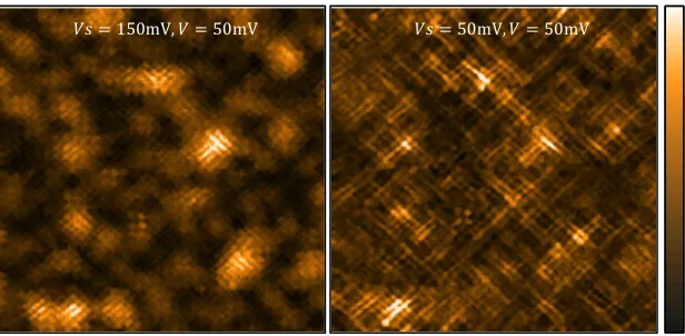
The figure below demonstrates how the choice of setup bias to establish the tunneling junction strongly influences the acquired data. While both the left and right panels are spatial images of the differential conductance taken at V = 50mV in the same field of view, the left was measured with Vs =150mV setup bias while the
right with Vs = 50mV. It is clear that the spatial intensity patterns of the same set of
We emphasize that the situation shown in Fig. S1 is not an unusual effect but rather is completely typical and unavoidable in all SI-‐STM studies, except under some specially prepared conditions (Section 6).
SI 3.
Predicted Fourier Transform STM Signatures of a dFF-‐DW
I – Sublattice Segregation Method to Determine DW Form Factor Symmetry
This section predicts the consequences of a primarily d-‐symmetry form factor density wave for the complex Fourier transform images of electronic structure on the three sublattices: Cu 𝒒 , 𝑂x 𝒒 ,𝑂y 𝒒 . In turn this controls the three key
functions used to measure modulations with different form factor symmetry as discussed in the main text.
𝑆 𝒒 = 𝐶𝑢 𝒒 (S3.1)
𝑆! 𝒒 = O
x 𝒒 +Oy 𝒒 2 (S3.2)
𝐷 𝒒 = Ox 𝒒 −Oy 𝒒 2 (S3.3)
Figure S1: Example of Setup Effect Two panels show the spatial differential conductance of
underoped BSCCO-‐2212 at 50mV acquired in the same field of view. The left panel was acquired with a setup bias of 150mV while the right with one of 50mV.
[image:30.612.148.456.62.213.2]A purely d-‐symmetry form factor density wave has modulations in anti-‐phase on the x and y oxygen sub-‐lattices (Fig. 1B of main text) and no modulation on the Cu site.
For the specific example of 𝑸𝒙 ≈ !!,0 , 𝑸𝒚≈ 0,!! considered in our study, this
requires that the peaks at ±𝑸𝒙 and ±𝑸𝒚 present in both Ox 𝒒 and Oy 𝒒 must
cancel exactly in 𝑆! 𝒒 = O
x 𝒒 +Oy 𝒒 2 and be enhanced in
𝐷 𝒒 = Ox 𝒒 −Oy 𝒒 2 . Conversely the peaks at Q’ = (1,0)±Qx,y and Q’’=(0,1)±
Qx,y will be enhanced in 𝑆! 𝒒 but will cancel exactly in 𝐷 𝒒 (Figs S2B,C).
This occurs because the two sub-‐lattices have modulations at the same wave-‐vector but with a π phase shift between them. Importantly, electronic structure images formed using the difference of oxygen sub-‐lattices, as in 𝐷 𝒒 , have the effect of removing this phase difference and recovering the peaks in the Fourier transform at the fundamental wave-‐vectors. These are necessary consequences of a density wave with a primarily d-‐symmetry form factor and hold for any d-‐symmetry form factor modulation in the presence of arbitrary amplitude and overall phase disorder.
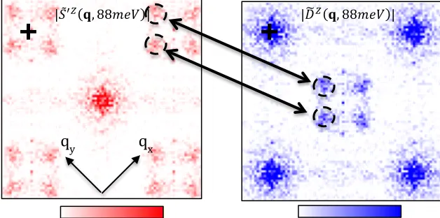
II –Form factor symmetry conversion of q5 for E > 𝜟𝟎
Fig. 3B of the main text shows the quasiparticle interference scattering vectors q1-‐q7
for energies below 𝛥! which are primarily s’FF symmetry modulations in the Z-‐map. Above this energy scale the dFF modulation appears, plotted in blue at 𝑄!!,!. This low-‐q modulation is extracted according to the scheme presented above by which the sublattice subtraction procedure of Ox and Oy reveals the density wave at its
primary wavevector. However, as seen from Fig. S2 B,C above, the physically identical dFF-‐DW can also be seen in the Ox(q)+Oy(q) at a q-‐vector which is
𝑄!!!,! = 1− 𝑄
!!,!. Thus, the same physical modulation will manifest at different but
related q-‐vectors in S’(q) and D(q). Figure S3 demonstrates this dual representation
of the same phenomenon. In Fig. 3B, the dFF-‐DW peak in S’(q) is plotted as 𝑄!!!,!
while that in D(q) is plotted as 𝑄!!,!; they represent the same physical dFF-‐DW modulation. In 𝑆′(𝒒 ) the dFF-‐DW modulation appears as 𝑄!!!,! ~ q
5(Δ0) persisting to
energies much larger than Δ0. In D(q) the identical physical modulation appears in
the same energy range at a wavevector 𝑄!!,! ~ q
1(Δ0) (Fig. 3F).
Figure S3: Equivalent representation of dFF modulations as Qs’ in the S’ and Qd in the D
channels.
qx qy
|𝑆!′!(𝐪,88𝑚𝑒𝑉)| |𝐷!!(𝐪,88𝑚𝑒𝑉)|
[image:33.612.164.478.445.601.2]