Heating Effect of Polycrystalline SiGe
/
Si Thin Films
on Phase Transition of GeSbTe Films
Seung-Yun Lee
+Department of Materials Science and Engineering, Hanbat National University, Yuseong-gu, Daejeon 305-719, Korea
This work reports the detailed manufacturing process of polycrystalline SiGe/Si thinfilm layers and their heating effect on phase transition
of GeSbTe chalcogenidefilms. The SiGe and Sifilms were grown successively by chemical vapor deposition, and different methods were
applied to dope the SiGefilms depending on their semiconducting nature because of phosphorus autodoping. Although the minimum dopant
concentration for the n-type SiGefilms was much higher than that for the p-type SiGefilms, the lowest transition currents were measured almost
same with both p- and n-type SiGefilms. The transition current decreased further with reducing contact area between the GeSbTe and SiGe
films. These results indicate that the contact area scaling and the formation of SiGe/Sifilms with a dopant concentration smaller than a critical
value are both required to induce the phase transition of GeSbTe at a submilliampere level of transition current.
[doi:10.2320/matertrans.M2013084]
(Received March 5, 2013; Accepted April 24, 2013; Published June 25, 2013)
Keywords: chalcogenide alloy, germaniumantimonytellurium, silicongermanium, phase transition, chemical vapor deposition, boron, phosphorus, doping
1. Introduction
The silicongermanium (SiGe) alloy has been widely used as a functional element in silicon-based microtechnology. The smaller band gap of SiGe than that of Si enables increase of current gain in a bipolar transistor, which leads to development of the high frequency SiGe heterojunction bipolar transistor.1,2) In addition, the relatively low thermal
conductivity of SiGe originating from its disordered alloy lattice makes the SiGe thin film applied as a thermoelectric component in IC-compatible thermoelectric microsystems.3)
It was recently found that the SiGe/Si heating electrode has a beneficial effect on decrease of the current required to induce phase transition of chalcogenide materials, namely, transition current.4) Since the power consumption of the GeSbTe phase change memory5) depends strongly on the transition current for the GeSbTe film, the reduction of the transition current has been a subject of considerable interest. The lower thermal conductivity and the higher electrical resistivity of SiGe compared to typical metals and their alloys are responsible for the effective joule heating and resulting phase transition of the chalcogenide material. It is generally believed that the precise control of the dopant concentration in the SiGe/Si electrode is very important to decrease the transition current because the resistive joule heating causing the phase transition is directly influenced by the resistivity of the electrode material. However, there are few systematic studies on the doping process of the SiGe/Si electrode which determines the dopant concen-tration and the corresponding resistivity. Thus, we inves-tigated the relationship between the manufacturing processes of SiGe/Si electrodes and the phase transition characteristics of GeSbTe chalcogenide alloys. Doping elements such as boron and phosphorus were doped into the polycrystalline SiGe/Si thinfilm layers prepared by low pressure chemical vapour deposition (LPCVD) and the contact structures of
sputter-deposited GeSbTefilms and the SiGe/Si multilayers were fabricated using conventional silicon semiconductor technology. The influence of the SiGe/Si multilayer formation on the phase transition of the GeSbTe films was examined with measuring transition currents and estimating dopant concentrations by secondary ion mass spectroscopy (SIMS).
2. Experimental Procedure
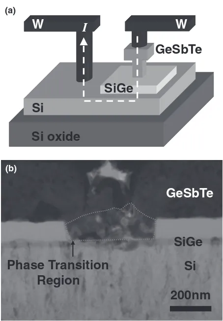
Figure 1(a) is the schematic diagram of the contact structure fabricated to determine the phase transition characteristics of GeSbTe films. 400 nm thick Si films and 40 nm thick SiGe films were deposited successively on Si oxide wafers by LPCVD and were patterned to form multilayer electrodes using separate photolithography steps. B2H6 and PH4 were used as a reactant gas to grow p- and
n-type SiGe/Si multilayers, respectively, in addition to the other gases such as SiH4, GeH4 and H2. The deposition
temperature was 923 K and the deposition pressure wasfixed to 4000 Pa. Tetraethylorthosilicate (TEOS) oxidefilms were prepared using LPCVD and contact holes were made through the TEOS oxide films by reactive ion etching. 300 nm thick GeSbTefilms were deposited by sputtering a GeSbTe alloy target and were defined using a conventional photolithog-raphy method. Tungsten pads were formed on the GeSbTe and Si films by typical steps such as via opens and metallizations. The microstructure of the contact structure was observed by transmission electron microscopy (TEM) and the dopant concentrations in the SiGe/Si multilayers were evaluated by SIMS. Resistance changes in the GeSbTe
films caused by applied voltage pulses were monitored using a semiconductor parameter analyzer. The voltage pulses whose amplitudes ranged from 0 to 9.9 V were applied to the contact structures and their width was fixed to 200 ns. The electric current flowing through the contact structures was directly measured using a current probe and a digital oscilloscope.
+Corresponding author, E-mail: sy_lee@hanbat.ac.kr
3. Results and Discussion
To induce phase transition of a GeSbTefilm, the heating electrode contacting with the GeSbTe film should be composed of the low-resistive and high-resistive conducting layers. The low-resistive layer plays a role in passing sufficient current required for causing the phase transition, and the high-resistive layer assists the phase transition by producing large amount of joule heat. In addition, the high-resistive layer retards the heat dissipation though the low-resistive layer due to its low heat conductivity.6)Figure 1(b)
is the cross-sectional view TEM image of the fabricated contact structure consisting of the sputter-deposited GeSbTe
film and the SiGe/Si multilayer electrode. This image was taken after the phase transition of the GeSbTefilm. The phase transition region having a coarse microstructure is observed in the GeSbTe film and the polycrystalline SiGe film is clearly distinguished from the columnar-grained Sifilm. The amorphous phase is not observed in the phase transition region due to the crystallization during the TEM sample preparation. However, the totally different microstructure between the phase transition region and the rest of the GeSbTe film suggests that the phase transition region is inferred as the original amorphous region. The dopant concentration in the SiGe film was much smaller that that in the Sifilm so that the SiGefilm acted as the high-resistive layer. Since the Si film was heavily doped as much as 1.0©1021cm¹3 and was much thicker than the SiGe film,
a large current could be supplied to the contact structure without a conventional metal electrode. To investigate the heating effect of the SiGe/Si multilayer electrode on the phase transition of the GeSbTe film, two kinds of SiGe/Si multilayers having different semiconducting natures were formed using LPCVD and postannealing processes. Firstly p-type SiGe/Si multilayer structures were prepared by an
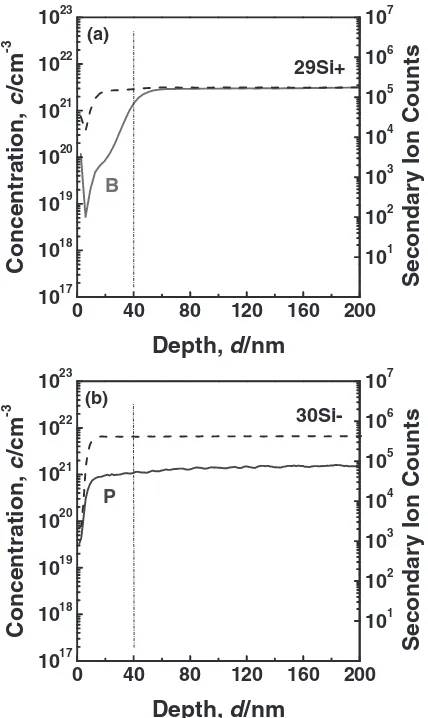
in-situ boron doping technique. Since the resistivity of the SiGe film increases and the heating effect also enhances with decreasing boron concentration, it is important to attain a low level of boron content in the SiGe film. The boron concentration as low as 2.9©1019cm¹3was readily achieved
by adjusting flow rates of B2H6, SiH4 and H2, as shown in
Fig. 2. Meanwhile it is noteworthy that the deposition time should be controlled for afixed thickness of SiGefilms due to the variable deposition rate resulting from the variation of B2H6 partial pressure. The inset of Fig. 2 clearly shows the
p-type multilayer structure composed of a lightly doped SiGe film with a boron concentration of 8.6©1019cm¹3 (at 300 nm depth) and a heavily doped Sifilm with a boron concentration of 2.0©1021cm¹3.
Secondly n-type SiGe/Si multilayer structures were formed by thermal diffusion of phosphorus into an intrinsic SiGe layer. Unlike the p-type SiGe/Si multilayer, thein-situ
doping method could not be used to prepare the lightly doped n-type SiGe layer because of phosphorus autodoping. Figures 3(a) and 3(b) are the doping profiles in the p- and n-type Si films in-situ doped with boron and phosphorus, respectively. The flow rates of reactant gases were changed during deposition in order to form the lightly doped and heavily doped regions in depth direction. In the case of the p-type Si film, the 40 nm thick lightly doped region was successfully grown on the heavily doped region. However, although it was intended to prepare lightly doped region at the surface of the n-type Si film, phosphorus atoms were heavily incorporated through the whole thickness. This autodoping of phosphorus is often observed in Si and SiGe deposited by CVD7,8) so that it is obvious that it is very
difficult to form the lightly doped SiGefilm directly on the
0 40 80 120
1017 1018 1019 1020 1021 1022 1023
B
29Si+ Ge
Depth,
d
/nm
Concentration,
c
/cm
-3
101 102 103 104 105 106 107
Secondary Ion Counts
0 1017 1018 1019 1020 1021 1022 1023
Lightly Doped SiGe
Heavily Doped Si B
29Si+ Ge
Depth, d /nm
Concentration,
c
/cm
-3
101 102 103 104 105 106 107
Secondary Ion Counts
120 80 40
Fig. 2 SIMS profile of the p-type SiGefilmin-situdoped with boron. The
inset shows the p-type multilayer structure composed of a lightly doped SiGefilm and a heavily doped Sifilm.
Si
SiGe
GeSbTe
200nm
(b)Phase Transition
Region
Si
W
W
Si oxide
SiGe
I
GeSbTe
(a)Si
W
W
Si oxide
SiGe
I
Fig. 1 (a) Schematic and (b) cross-sectional view TEM image of a contact
structure including a polycrystalline SiGe/Si multilayer and a GeSbTe
[image:2.595.55.282.65.391.2] [image:2.595.313.540.66.259.2]heavily doped Si film. Thus the n-type SiGe/Si multilayer structures were fabricated in two steps: successive deposition of the heavily doped Si and intrinsic SiGe films and postannealing to diffuse phosphorus from Si into SiGe. Figure 4 shows the n-type multilayer structures composed of lightly doped SiGefilms and heavily doped Sifilms. A large amount of phosphorus was detected even in the as-deposited SiGefilm and the phosphorus concentration increased from 1.9©1020 to 3.0©1020cm¹3 (at 300 nm depth) with
increasing postannealing temperature from 1123 to 1148 K. The phosphorus concentration monotonously increased from the surface to the Si film, and no plateau was seen in the concentration curve for phosphorus unlike that for boron in Fig. 2, which corresponds to a typical doping profile caused by a thermal diffusion process. Table 1 summarises the dopant concentrations in and the resistivities of the SiGe
films prepared on the heavily doped Si films. The n-type SiGefilms doped by thermal diffusion had a narrower range of dopant concentration and resistivity than the p-type SiGe
films doped using anin-situdoping technique. The resistivity of the p-type SiGe films increased after annealing in an N2
ambient due to the BN formation9)so that it could be elevated
much further by the annealing treatment.
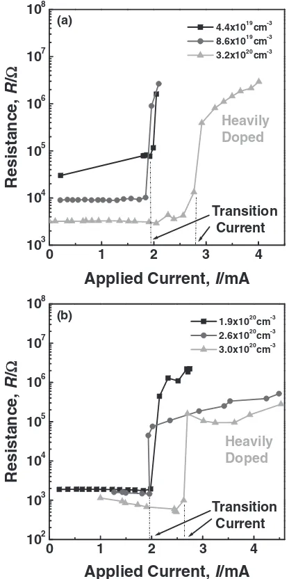
The transition currents needed to cause the phase transition of the GeSbTe film were compared for the SiGe/Si
multilayers with different dopant concentrations. Figure 5 shows resistance changes of the contact structures with increasing applied current. The abrupt resistance increase at the critical current value results from the phase transition of the GeSbTe film from the crystalline to amorphous states. GeSbTe is a chalcogenide alloy having a relatively high resistivity in an amorphous state several hundred times larger than that in a crystalline state.10) When a current pulse is applied to the contact structure consisting of the crystalline GeSbTefilm and the SiGe/Si multilayer, joule heat propor-tional to (current)2·resistance is generated. If the current smaller than the critical value is delivered, a relatively low resistance value corresponding to the crystalline phase of GeSbTe remains for lack of joule heat causing the phase transition. However, if the applied current reaches to the critical value, then the part of the crystalline GeSbTe film transforms to amorphous by means of a melt-quench process11) and the resistance increases drastically above
105ohm, as shown in Fig. 6. Since the joule heat generated
from the high-resistive SiGefilm assists the temperature rise in the GeSbTefilm, the SiGe/Si multilayer electrode plays a significant role in decreasing transition current. The transition current decreased and then saturated with decreasing dopant concentration irrespective of electrode’s semiconducting nature, as shown in Fig. 5. In the case of the heavily doped electrode, large transition current was required to induce the phase transition due to its low resistivity. On the other hand, the transition current was fixed to about 2.0 mA with the dopant concentrations of 8.6©1019cm¹3and less for the
p-type electrode, and of 2.6©1020cm¹3and less for the n-type
electrode. The reason for the ineffectiveness of the very
1017
1018
1019
1020
1021
1022
1023
(a)
B
29Si+
Depth,
d
/nm
Concentration,
c
/cm
-3
101
102
103
104
105
106
107
Secondary Ion Counts
0 40 80 120 160 200
0 40 80 120 160 200
1017
1018
1019
1020
1021
1022
1023
(b)
P
30Si-Depth,
d
/nm
Concentration,
c
/cm
-3
101
102
103
104
105
106
107
Secondary Ion Counts
Fig. 3 SIMS profiles of the p- and n-type Sifilms in-situ doped with
(a) boron and (b) phosphorus.
0 40 80 120 160 200
1017
1018
1019
1020
1021
1022
1023
As-deposited 1123K 1148K
P
30Si-Ge
Depth,
d
/nm
Concentration,
c
/cm
-3
101
102
103
104
105
106
107
Secondary Ion Counts
Fig. 4 SIMS profile of the n-type multilayer structures composed of lightly
[image:3.595.63.277.69.428.2]doped SiGefilms and heavily doped Sifilms.
Table 1 Comparison of dopant concentrations in and resistivities of two
types of SiGefilms.
Dopant concentration,
c/cm¹3
Resistivity,
µ/mohm·cm
Boron doped SiGe 4.4©10193.2©1020 6189135
[image:3.595.314.532.70.250.2] [image:3.595.305.549.331.383.2]lightly doped SiGe/Si electrode in reducing transition current attributes to the inherent property of semiconductor whose resistivity decreases with a temperature rise,12)for example,
caused by joule heating. As the contact area between the
GeSbTe and SiGe films decreased from 1.0©1.0 to
0.5©0.5 µm2, the transition current decreased further, as
shown in Fig. 7. Since the current density is larger in the smaller contact area at the same current level, the joule heating in the electrode and the GeSbTe film is greatly enhanced. Thus the temperature of the GeSbTefilm may be easily reached to its melting point with a smaller current in the case of the smaller contact area. This relation between transition current and contact area suggests that a low level of transition current can be achieved by both the formation of the electrode containing a dopant concentration smaller than a critical value and the contact area scaling using sophisti-cated fabrication processes.
103
104
105
106
107
108
Transition Current
Heavily Doped (a)
Resistance,
R
/
Ω
Applied Current,
I
/mA
4.4x1019cm-3
8.6x1019cm-3
3.2x1020cm-3
4
0 1 2 3
0 1 2 3 4
102
103
104
105
106
107
108
Transition Current
Heavily Doped (b)
Resistance,
R
/
Ω
Applied Current,
I
/mA
1.9x1020cm-3
2.6x1020cm-3
3.0x1020cm-3
Fig. 5 Dependence of phase transition characteristics of GeSbTefilms on
dopant concentrations in SiGe films: (a) p-type SiGe/Si samples and
(b) n-type SiGe/Si samples. The contact areas between the GeSbTe and
SiGefilms werefixed to 1.0©1.0 µm2.
Applied Current
Resistance
Amorphous GeSbTe
Crystalline GeSbTe Amorphous GeSbTe
Crystalline GeSbTe
Fig. 6 Schematic of the phase transition in GeSbTe and the resulting
resistance change induced by applied current.
103
104
105
106
107
108
(a)
Resistance,
R
/
Ω
Applied Current,
I
/mA
1.0x1.0μm2
0.5x0.5μm2
3
0 1 2
0 1 2 3
102
103
104
105
106
107
108
(b)
Resistance,
R
/
Ω
Applied Current,
I
/mA
1.0x1.0μm2
0.5x0.5μm2
Fig. 7 Dependence of phase transition characteristics of GeSbTefilms on
contact areas between the GeSbTe and SiGe films: (a) p-type SiGe/Si
samples and (b) n-type SiGe/Si samples. The dopant concentrations in the
p- and n-type SiGefilms werefixed to 8.6©1019and 1.9©1020cm¹3,
[image:4.595.323.529.67.486.2] [image:4.595.65.273.71.487.2] [image:4.595.55.285.607.759.2]4. Conclusion
Contact structures of the sputter-deposited GeSbTe films and the SiGe/Si multilayer electrodes were fabricated so as to determine the effect of the SiGe/Si thinfilms on the phase transition of the GeSbTe films. The SiGefilms were lightly doped for resistive joule heating, whereas the Si films were heavily doped higher than 1.0©1021cm¹3 for sufficient current conduction. The p-type SiGe/Si multilayer structures were readily prepared usingin-situboron doping, but thisin
-situ doping method could not be used for the n-type ones because of the phosphorus autodoping from the heavily doped Si films during SiGe deposition. Thus the n-type SiGe/Si multilayer structures were fabricated in two steps, intrinsic SiGe deposition and postannealing. Resistance changes in the contact structures with different applied currents were measured, and it was confirmed that the SiGe/Si multilayer electrodes doped below 3.0©1020cm¹3
resulted in a significant decrease of the transition current irrespective of their semiconducting natures. The effect of transition current reduction became further prominent with decreasing contact area between the GeSbTe film and the SiGe/Si multilayer electrode. These results suggest one possible pathway towards low power GeSbTe phase change memory by controlling the dopant concentration in the
SiGe/Si multilayer electrodes in addition to contact area scaling.
REFERENCES
1) E. Ojefors, B. Heinemann and U. R. Pfeiffer: IEEE Trans. Microw.
Theory Tech.59(2011) 13111318.
2) S.-Y. Lee, C. Zhu, J. D. Cressler and S.-H. Lee:Jpn. J. Appl. Phys.47
(2008) 53095313.
3) Z. Wang, J. Su, Y. van Andel, H. Nguyen and R. J. M. Vullers: Proc. 16th International Solid-State Sensors, Actuators and Microsystems
Conference, (2011) pp. 346349.
4) S.-Y. Lee, K.-J. Choi, S.-O. Ryu, S.-M. Yoon, N.-Y. Lee, Y.-S. Park,
S.-H. Kim, S.-H. Lee and B.-G. Yu:Appl. Phys. Lett.89(2006) 053517.
5) S.-Y. Lee, Y.-S. Park, S.-M. Yoon, S.-W. Jung, J. Lee and B.-G. Yu:
Microelectron. Eng.85(2008) 23422345.
6) I. V. Karpov and S. A. Kostylev:IEEE Electron Device Lett.27(2006)
808810.
7) M. Tanimoto, J. Murota, M. Wada, T. Watanabe, K. Miura and N. Ieda:
IEEE J. Solid-State Circuits17(1982) 6268.
8) S. P. Murarka:J. Appl. Phys.56(1984) 22252230.
9) M. Ylönen, A. Torkkeli and H. Kattelus:Sens. Actuators A Phys.109
(2003) 7987.
10) S. Braga, A. Cabrini and G. Torelli: Appl. Phys. Lett. 94 (2009)
092112.
11) Y. S. Park, J. W. Lim, W. S. Yang, S.-Y. Lee, S.-M. Yoon and B. G. Yu:
Mater. Trans.49(2008) 21072111.
12) S. O. Kasap:Principles of Electronic Materials and Devices, 3rd ed.,