Effects of Initial Punch-Die Clearance in Spark Plasma Sintering Process
Salvatore Grasso
1;2;3;*1,*2, Yoshio Sakka
1;2;3and Giovanni Maizza
41Graduate School of Pure and Applied Sciences, University of Tsukuba, Tsukuba 305-0047, Japan
2World Premier International Research Center Initiative (WPI Initiative) on Materials Nanoarchitronics (MANA),
NIMS, Tsukuba 305-0047, Japan
3Nano Ceramics Center National Institute for Materials Science (NIMS), Tsukuba 305-0047, Japan 4Dipartimento di Scienza dei Materiali ed Ingegneria Chimica, Politecnico di Torino,
Corso Duca degli Abruzzi 24, I-10129 Torino, Italy
In recent years the number of publication on SPS has grown exponentially although the process itself is still not completely understood. The SPS process is governed by a complex bulk and contact multiphysics. The contact resistance between SPS system elements is crucial to understand the overall current and temperature distribution. This work is undertaken in order to improve our fundamental understanding on the contact resistance behaviour in the SPS system. The effect of the initial punch-die clearance is experimentally investigated for the first time during SPS heating. The results are given in terms of temperature-time and voltage-time profiles for various clearance values. It is shown that the initial punch-die clearance is a key SPS parameter to be specified when different SPS experiments or apparatus features have to be compared and offers another means to control the temperature gradient along the radius. [doi:10.2320/matertrans.MER2008263]
(Received August 8, 2008; Accepted October 7, 2008; Published November 25, 2008)
Keywords: spark plasma sintering, vertical contact resistance, punch-die clearance, temperature gradients, contact tightness
1. Introduction
In recent years the number of publications on Spark Plasma Sintering (SPS) has grown considerably,1)due to its inherent advantages, such as faster densification, limited grain growth, shorter sintering time and lower sintering temperature in comparison to conventional hot pressing.1–4)
Despite the number of SPS studies and the number of successfully consolidated material systems, the achieved fundamental understanding of SPS phenomena is still unsatisfactory. This translates into practical difficulties such as lack of finding optimum punches/die design, select optimum operating conditions (i.e. current, temperature, pressure and heating rate) or lack of control temperature gradients along the radius. It is reported that the latter typically determines inhomogeneous microstructures and non-uniform properties.5,6) Besides, inhomogeneous
micro-structures are generally critical for industrial scale applica-tions, especially for the consolidation of large compacts.7,8)
From an experimental point of view the lack of SPS control is mainly caused by measurement difficulties, especially, temperature measurement ones. Usually, an optical pyrometer is employed to measure the outer dies surface temperature while the sample core temperature measurement would be much more desirable. Vanmeensel
et al.9)have succeeded in monitoring temperature nearby the
sample edge using a double pyrometer system. Alternatively others authors10) have used thermocouples to measure
temperature at the sample edge. However, so far accurate temperature measurements are proved only using compact samples rather than actual powders. Thus the understanding of SPS phenomena during densification is still an open question to research.
Realistic modeling of SPS is difficult due to intrinsic
complex interaction between bulk and contact multiphysics phenomena (i.e. electric, thermal, stress-strain, kinetic). While bulk multiphysics is well documented in the SPS literature,9–12) contact multiphysics is still veiled both experimentally and computationally.
SPS contact interfaces act as sources of Joule heating which evolution depends primarily on the tightness of the joint. In addition contact interfaces are strongly coupled with bulk (electric and thermal) field, especially near the interface. This occurs even in the case of ideally clean and uniform contact surfaces. The simultaneous influence of bulk and contact electrothermal phenomena in SPS has been already investigated.9–12) For instance Zavaliangos et al.10) solve a
coupled electrothermal model and estimate the SPS contact resistance system during heating of an alumina compact. They classify the SPS contact resistances into horizontal and vertical ones and found that the vertical contact resistances are much larger than horizontal ones. Cincotti et al.11)
simulate the SPS heating of a graphite compact using a coupled electrothermal model. They ignore the influence of vertical contact resistances and confirm both, computa-tionally and experimentally, that SPS horizontal contact resistances are negligible. Vanmeensel et al.9,13) simulate
the SPS heating of conductive and insulating compacts (i.e., 3Y-ZrO2, graphite and TiN) using an electrothermal bulk model. The effects of horizontal contact resistances are here taken implicitly into account by adjusting the simulation results with experiments. Instead, they succeed in measuring the temperature nearby the sample edge, using a double optical pyrometer system. In addition they succeed experimentally to assess the leading role of the horizontal and vertical contact resistances, as a function of temperature and currents.
Maizzaet al.5)developed a SPS model which fully couples the electrothermal and displacement (shrinkage) fields using a finite element moving mesh technique. In this case the SPS phenomena are simulated during sintering of a WC powder. *1Ph.D. Student, University of Tsukuba
*2Corresponding author, E-mail: [email protected]
Particularly they have determined how the vertical contact resistance changes in time during the relative sliding of the punch/die contact surfaces. An experimentally intensive calibration procedure is necessary to validate the overall procedure and to evaluate all SPS contact resistances as a function of temperature. They pointed out that the (vertical) punch-die contact resistance is the most important factor which controls the SPS process, especially the transient heat generation in the punch/die/sample assembly.
One aspect of the SPS contact resistance being ignored so far concerns the role played by the initial clearance between punch/sample/die contact surfaces on the overall assembly temperature distribution. Clearances are joint gaps that exist in a variety of mechanical and electrical applications. They are often inevitable due to machining tolerances. However, clearances may also change because of wear, materials deformations or imperfections. In the SPS apparatus, the initial clearance may play a significant role along vertical interfaces. However, it may have little effect along horizontal contact interfaces. In the latter case, depending on the applied pressure, the contact resistance can be minimized since the pressure can make the joints very tight mechanically, thus enhancing the current and the heat flow across the joint. This consideration is in agreement with several modeling works.9–12)On the other hand, the applied pressure does not
influence the vertical contact interfaces, at least to a first approximation, unless (secondary) Poisson effects. Thus, we may assume that the applied pressure does not affect the initial clearance, consequently the initial clearance effects and the applied pressure effects can be decoupled. This simplification makes the initial clearance effects worth of studying individually and independently by other factors. According to previous results5) the (vertical) punch-die
interface exhibits the largest vertical contact area in the SPS apparatus with the largest influence on heating and sintering. Therefore the changes in the initial clearance along this interface may impact noticeably on the contact resistance changes.
To the authors’ knowledge, no papers have been found on the effect of the initial punch/die clearance on electric and thermal vertical contact resistances, neither the initial punch/ die clearance has been considered as a basic specification for SPS experiments.
2. The Punch-Die Contact Resistance and Clearance Effects
Graphite is often used in SPS devices as an effective contact material, particularly in sliding conditions, due to its high electric and thermal conductivity, oxidation and wear resistance. Its loading capacity is however limited to 80– 150 MPa. During SPS heating, elastic and plastic defor-mation of the contact asperities may induce reversible or irreversible changes in the contact area. The electric contact resistance is related to contact area according to the equation10)
Rc¼1=ðAcGÞ
whereAC (m2) is the contact area andG (1m2) is the
electric gap conductance.
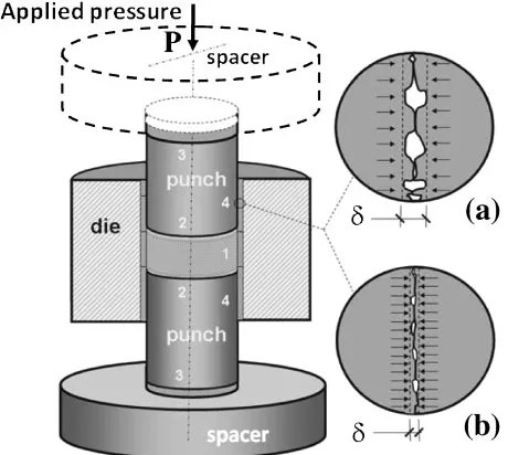
In electrical applications the presence of excessive joint gaps can lead to ineffective current flow across the interface. In some circumstances they can even cause arching. The clearance ratiois defined as:
¼100%ðDdÞ=D
where D is die diameter and d is punch diameter. In this work, the value of d is specified by design while D and applied loadPare held constant throughout.
Figure 1 shows (a) sketch of a loose and (b) close clearance along the (vertical) punch/die contact interface. Too small a clearance may cause excessive seizing. Con-versely, too large a clearance may excessively increase the contact resistance. The electric behaviour of aclose contact
couple may significantly differ from that of aloose contact
couple, even in the ideal case that the two contact surfaces are perfectly conductive. The initial clearance values can be defined initially by design, although during service operation its value may change to some extent with direct consequen-ces on the overall heat generation, heat transfer and current flow from the sample-punch assembly to the die.
Graphite is particularly susceptible to service wear, abrasion, scratching, etc. For instance, the die/powder interface is subjected to repeated scratches during sample extraction especially in the case of high applied pressure. The initial punch/die clearance typically equal to 0.05 mm may increase after each run of approximately 0.1 mm.
3. Experimental Procedure
[image:2.595.313.543.73.279.2]punches and the sample are here made of low strength graphite commercially known as molded graphite GS-203 (supplied by Syntex Inc., Japan). The outer and inner diameters of the die are 50 and 20 mm respectively. Its height is 40 mm. The nominal diameter and thickness of the graphite disk are 20 mm and 8 mm respectively. The punch diameter is turned to19.80, 19.90, 19.95 and 19.98 mm to provide four different initial clearances, (e.g. 0.2, 0.1, 0.05, 0.02 mm respectively) at the punch-die interface contact. The punch height is assumed to be of 20 mm. The reference value for the initial clearance is assumed to be 0.05 mm. Three couples of spacers made up molded graphite GS-203 were employed, diameters and heights h (mm) were respectively80 h 40,100 h 20 and120 h 20.
The flexural strength, the tensile strength, the elastic modulus and the Shore hardness of graphite is 50 MPa, 26 MPa, 9.3 GPa and 60, respectively, as provided by the manufacturer. Experiments in this work are carried out under CCM. This operation mode is selected since it offers a direct and a systematic means to evaluate the contact resistance system during SPS experiments. In addition, CCM offers an effective method to compare the contact resistance system of various SPS apparatuses.
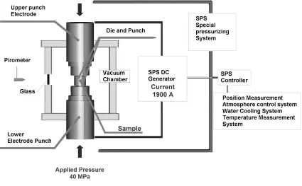
The applied pressure and DC current are assumed to be constant and equal to 40 MPa and 1900 A, respectively. All experiments are carried out under vacuum conditions. For caution reasons, the heating process is interrupted until the peak temperature reaches about 1850C. Experiments are repeated twice to permit the temperature recording at two different points, e.g. at the die surface and at the sample edge (i.e. A and B respectively, in Fig. 3), using only one optical pyrometer. The reasons for this choice will be discusses later. The borehole of point B is obtained by drilling a 7 mm diameter hole across the die radius down to the sample/die interface location. During the SPS experiments both punches
are assumed to be fixed and so are the locations of the temperature probes (A and B). The pyrometer (Chino IR-AHS) spot size is 3 mm in diameter at the measuring distance is 300 mm apart from the die surface.14)The second run is also used to check for experiment reproducibility in terms of voltage. In all experiments the voltage drop was recorded across the entire system via the default control panel of SPS machine.
The choice for using only one single optical pyrometer for measuring two different points, thus repeating each experi-ment twice has the advantage that the two temperature measurements are naturally correlated, since the same pyrometer is used. However, this measurement strategy assumes that the SPS experiment is repeatable. Preliminary experiments have proved that this assumption is frequently fulfilled, although several cautions have to be taken into account to assure the same experimental conditions at each run.
Before restarting a new run the graphite elements are cooled down for more than 60 minutes. The diameter of the blind hole (B point) is 7 mm, e.g. measuring area is five times larger than the spot pyrometer size (3 mm diameter), to assure Fig. 2 Schematic of SPS apparatus.
[image:3.595.86.511.73.336.2]reliable temperature measurements. To minimize radiation heat loss effects a 2.5 cm thick graphite felt is used. Experiments are conducted with and without the graphite felt to inspect clearance effects without any influence of radiation heat losses.
4. Results
Four initial punch/die clearance values, say, 0.2, 0.1, 0.05 and 0.02 mm, corresponding to punch diameters 19.80, 19.90, 19.95 and 19.98 mm, are investigated. The 0.05 mm clearance is taken as a reference, as normally assumed in SPS hardware construction (Syntex Inc., Japan).
Each clearance experiment consists of four runs: a) temperature measurement at A point; b) assessment of experiment repeatability at A point; c) temperature measure-ment at B point; d) assessmeasure-ment of experimeasure-ment repeatability at B point. However, carbon felt is normally used in SPS experiments to reduce radiation losses at the die surface. The presence of such felt normally causes considerable changes in the temperature field.5,15)Therefore, two additional runs
are required, for each clearance, to record temperatures at A and B, when carbon felt is applied.
4.1 Effect of clearance on electric contact resistance Figure 4 shows the voltage profile recorded during heating for different initial punch/die clearances using constant applied current (1900 A) and pressure (40 MPa). As the current intensity is held constant in current control mode, the measured voltage profile is identical to the electric resistance profile. In Fig. 4 the voltage progressively decreases with decreasing of clearance. The voltage profile is lower for the smaller clearance (0.02 mm). As others parameters are held constant, the progressive decrease of voltage is only attributed to clearance decrease or, identically, to contact resistance decrease. Therefore, the smaller the clearance, the lower the voltage and the contact resistance at the punch/die interface. With this concern, McWilliamset al.15)report that
electric current density inside punches is one order of magnitude higher than that inside the die because of the effect of punch/die contact resistance. This observation is also in agreement with previous experimental and computational works.5,10) For instance, Zavaliangoset al.10)show that the
vertical contact resistance plays a dominant role on the current distribution across the punch/sample/die assembly; thereby the lower electric contact resistance at the punch/die interface enhances the current flow towards the die. As a result, the voltage decreases due to the higher overall electric resistance of punches compared to that of the die. Accurate predictions of contact phenomena are desired to correctly determine the current distribution in the punch/sample/die assembly.
4.2 Effect of clearance on sample and die surface temperatures
4.2.1 Effect of insulating felt
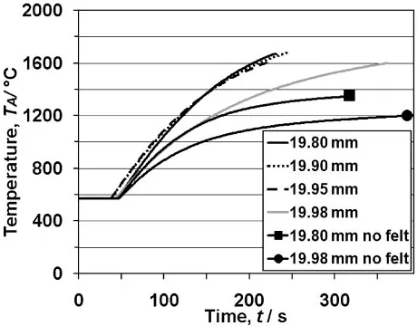
Figures 5 and 6 show the temperature recorded during SPS heating at the sample edge (B) and at the die surface (A) respectively with and without insulating felt. As Joule heating is directly proportional to current intensity and voltage drop and the supplied current is constant, the changes in heating will directly relate to changes in voltage drop. In
Fig. 4 Voltage drop between the two rams as a function of time for different punches diameters.
Fig. 5 Temperature as function of time measured at die surface point (point A) for different values of punches diameters with and without insulating felt.
[image:4.595.311.541.325.505.2] [image:4.595.311.541.568.748.2] [image:4.595.55.285.611.758.2]the case of 0.02 mm clearance the voltage drop is 0.5 V smaller than that obtained with 0.1 mm clearance. For sake of clarity, only two temperature profiles (for 0.02 and 0.2 mm clearances) are drawn in Figs. 5 and 6. By comparing Figs. 5 and 6 we notice that recorded temperatures in B are greater than those in A for each clearance value. This confirms the natural development of radial temperature gradients during SPS heating of conductive compact samples.5,9–11)At the end
of SPS heating the temperature difference between A and B is approximately of 200 and 400C for 0.02 and 0.2 mm clearance respectively. The larger the initial clearance, the larger are the recorded temperatures at both A and B. It is observed that the temperatures measured in B contain more information than those in A. Indeed, the temperature profiles in Fig. 5 show approximately all the same behavior in A for each initial clearance value, with exception of the curve for 0.02 mm clearance. By contrast, the same curves in Fig. 6 are all different, showing different rates and peak temperatures. This proves the greater importance of B point as probe point for tracing SPS, especially contact phenomena. By compar-ing the temperature profiles in Fig. 6, we notice that the observed larger temperatures for result directly from the larger contact resistance induced by the larger initial punch/ die clearance. The larger the electric contact resistance, the larger will be the heat dissipated at the contact per unit of time and the larger will be the heating rate and the temperature peak at the interface. This behaviour is clearly shown in Fig. 6 for each clearance value. By contrast, the smaller initial clearance shows a very different situation due to the relatively small induced contact resistance. In this case, the temperature evolution in B is mainly attributed to the larger current and heat flow crossing the contact interface than contact phenomena. These preliminary results prove the non linear relationship existing between thermal field evolution and initial punch/die clearance (or contact resist-ance). Accordingly, the transient heating of the punch/ sample/die assembly is expected to be significantly influ-enced depending on whether a large or small punch/die clearance is employed initially.
4.2.2 Effect of no-insulating felt
It is generally reported that the absence of felt promotes the development of much higher radial temperature gradi-ents.5,15) In Fig. 5 the temperature profiles for only two clearance values are reported for sake of clarity. These temperature profiles correspond to 0.02 and 0.2 mm clear-ances, respectively. It is observed that the absence of felt causes a dramatic decrease of temperatures, in both A and B. For instance, the temperature difference caused by the absence of felt, in comparison to the presence of felt, after 200 s at A/B points for 0.2 and 0.02 mm clearance is about 320/225 and 236/200C respectively. The largest temper-ature difference is observed at the radiating die surface (A) for each clearance. For instance, it is 319 and 236C for 0.2 and 0.02 mm clearance, respectively. However, the sample edge (B) is also affected by the absence/presence of felt, though to a minor extent, e.g. 225 and 199C for 0.2 and 0.02 mm clearance, respectively. Vice versa, the initial punch/die clearance effect may be even enhanced by the presence/absence of felt. Thus, the initial punch/die clear-ance and the presence of felt are two key SPS factors that non
linearly affect the temperature and thus have to be specified when SPS experiments are quantitatively compared.
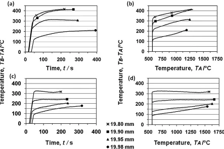
4.3 Effect of clearance on radial temperature gradients Figure 7 shows the effective temperature difference (TAB ¼TBTA) profiles as a function of time (Figs. 7(a),
7(c)) and of die surface temperature (Figs. 7(b), 7(d)) in the case of felt (Figs. 7(c), 7(d)) and without felt (Figs. 7(a), 7(b)). Note that Fig. 7(a) and 7(d), in contrast with Figs. 5 and 6, show temperature profiles with and without felt for all investigated initial punch/die clearances. These profiles are obtained by subtracting for each clearance the temperature profile in Fig. 6 by the corresponding profile in Fig. 5. The
effective temperature differenceTAB (hereinafter,
temper-ature gradient) actually includes two contributions, namely, the temperature difference over the die thickness and the temperature jump at the punch/die contact gap.
The temperature difference between A and B increases with increasing of temperature and heating times, due to larger radiation losses, and is larger in the absence of felt, at each clearance value.
This different temperature behaviour caused by different initial punch/die clearances holds true regardless the pres-ence/absence of felt, although the absence of felt normally acts in such a way that clearance phenomena will be slightly depressed due to reduced temperature field.
4.3.1 Effect of insulating felt
Figures 7(c) and 7(d) show that the thermal gradient profiles may be split into two periods in time, a first stage (linear) and a second stage (non-linear). The thermal gradient rate is about 10C/s during first stage and holds constant regardless the initial clearance value. This thermal gradient rate compares well with the heating rate of the process taken from Fig. 5. This confirms that during first stage the thermal gradient evolution is mainly controlled by interface temper-ature (B). The ending time of first stage is approximately the same (i.e. 45 s) regardless the initial clearance. In Fig. 7(c) the thermal gradients, for 0.2 and 0.1 mm initial clearances, evolve similarly, however, at the end of first stage the thermal gradient is larger for 0.2 than for 0.1 initial clearance (i.e. 325 vs. 225C). By contrast, the evolution of thermal gradients with 0.05 and 0.02 mm initial clearances are slightly delayed with respect to the former (0.2 and 0.1 mm) initial clearance values and the thermal gradients at the end of first stage are much smaller than before, e.g. about 120 vs. 95C, for 0.05 and 0.02 mm initial clearance respectively. The thermal gradients caused by smaller clearances evolve with relatively large delay (32 s). The thermal gradients in second stage, after 200 s, are larger for larger initial clearances, i.e.320, 244, 200 and 150C for 0.2, 0.1, 0.05 and 0.02 mm initial clearance respectively.
4.3.2 Effect of no-insulating felt
(B) control the first stage of heating. The thermal gradient evolution for 0.02 mm initial clearance is different in nature from previous developed by larger initial clearances.
A strong increase of thermal gradient with time is observed (Fig. 7(a)). The thermal gradient profiles for 0.2 and 0.02 mm initial clearance respectively depart with time. The radiation losses at the die surface lower significantly the die surface temperature so that the overall temperature difference between A and B points is significantly enhanced. The larger gradient is observed at the higher temperatures, for both clearances. By comparing the system behavior with Fig. 7(c) and without insulating felt Fig. 7(a) for the smaller and larger clearances, we notice that a larger gradient (about 100C) is observed with a larger clearance (0.2 mm) while relatively small gradient (about 40C) is observed with a smaller clearance (0.02 mm) after 200 s.
4.4 Effect of clearances on temperature gradient and die surface
4.4.1 Effect of insulating felt
Figures 7(b) and 7(d) relate the developed thermal gradients to the currently measured surface temperature (A) for various initial punch/die clearances. Figure 7(b) clearly shows as the surface temperature (A) is insufficient to explaining bulk SPS phenomena since very high and variable thermal gradients originate at least when conductive samples are processed. These thermal gradients are strongly affected by the application of felt and the value of initial punch/die clearance. Such thermal gradients may achieve at the end of heating values as high as 325 or 240C for 0.2 or 0.1 mm initial clearances, although they remain constant in all second
stage, regardless the value of surface temperature. On the other hand, thermal gradients are relatively smaller, say, 200 or 170C, at the end of heating, for 0.05 or 0.02 mm initial clearances respectively, although they show a slight linear increase with surface temperature during second stage.
The detailed evolution of thermal gradients during heating is clearly shown in Fig. 7(d). This figure appears qualita-tively similar to previous one Fig. 7(b) as a function of surface temperature. It has the advantage to show both stages of heating and rate of thermal gradients during heating for each initial clearance. This Figure confirms the different behaviour of larger initial clearances (0.2 and 0.1 mm) with respect to smaller initial clearance (0.05 and 0.02 mm). The former are relatively larger but constant in time, the latter are relatively smaller but increase with time.
4.4.2 Effect of no insulating felt
Figures 7(a) and 7(b) show the thermal gradients counter-part in the case of no applied felt. As can be seen the thermal gradients are much larger (400C) and the surface temper-ature at the end of heating is much smaller (1250C) than those observed with felt (325 and 1700C, respectively). The peak temperatures at the end of first stage are much higher at all initial clearances. In Fig. 7a, the evolution of thermal gradients for larger initial clearances (0.2, 0.1 and 0.05 mm) is less stressed in comparison to that in Fig. 7(c) (with felt). Actually these profiles share the same first stage, although with different peak temperatures at the end of it. However, they are much closer to each other than those originated with felt. The second stage, instead, is similar for the two larger initial clearances (0.2 and 0.1 mm) but substantially different for intermediate (0.05 mm) and smaller (0.02 mm) initial Fig. 7 Temperature difference without (a), (b) and with (c), (d) insulating graphite felt between sample edge (B) and die surface (A) as
[image:6.595.76.519.71.367.2]clearances. Substantially different, instead, is the behaviour of 0.02 mm initial clearance in the first and second stage of heating compared to previous three profiles. At the end of heating, the thermal gradient developed in this case (without felt) compares well with that observed in Fig. 7(c) (205 vs. 175C), although the heating times are inevitably different in both cases (400 vs. 320 s). The same considerations can be made on thermal gradients by inspecting Fig. 7(b) as a function of surface temperature. This figure highlights as much larger gradients can be developed when heating without felt than with felt, mainly resulting from the smaller surface temperatures during heating. Another unique feature observed in Figs. 7(a) and 7(b) is that the thermal gradients in second stage of heating (without felt) are neither constant with time nor with surface temperature as, instead, shown in Figs. 7(c) and 7(d).
5. Discussion
The results above make clear as the contact phenomena along the vertical punch/die interface can be influenced by the initial fit clearance and as may influence the overall stage of heating of conductive compact samples. The selected CCM operation of SPS offers a direct and systematic means to characterize SPS experiments and hardware features. In addition the CCM allows short heating cycle to be studied and the influence exerted by high heating rates to be assessed in detail. However, current control mode may promote large thermal gradients along the radius, as observed during heating of conductive samples. Accordingly, CCM may invoke a more substantial role of contact resistance in the SPS system, especially during the initial transient (e.g. first stage) of heating. Therefore, CCM is conveniently used here to characterize the behaviour of contact interfaces in a SPS system.
Temperature gradients in the die may be promoted by two concurring phenomena: heat generation and heat conduction. Heat generation may occur either in the bulk or at the contact interfaces. In the SPS, the latter is mainly controlled by the punch/die contact resistance.5) In this work, the contact
resistance is intentionally changed by changing on the initial punch/die clearance. Heat conduction inside the punch/die/ sample assembly can be enhanced by assuring a good punch/ die contact as shown by smaller initial clearances (0.02 mm), with and without felt. On the other hand, heat generation can be enhanced by allowing larger contact resistances, e.g. via larger initial clearances (either 0.2 or 0.1 mm. Another important factor in SPS, being responsible for the develop-ment of thermal gradients along the radius, is felt.
From Fig. 7 we observe that the smaller clearance (0.02 mm) always promotes (with felt and without felt) a good electric and thermal contact across the punch/die interface. Consequently, resistive heating inside the punch/ sample/die assembly decreases as shown in Fig. 4 by voltage measurements. On the other hand, the behaviour of larger initial clearances differs, even to a large extent, depending on whether the felt is applied or not. In general, the established thermal gradients across the die are larger for the larger initial clearances and may exceed 400 or 300C with felt or without felt, respectively.
The radial temperature gradients have been determined by various authors both numerically and experimentally during SPS heating10,12,16,17)and sintering5)using compact
conduc-tive samples. They find that the temperature gradients increase linearly with the die surface temperature (A) which is in agreement with Figs. 7(b) and 7(c).
Although more investigations are required to elucidate the phenomena contributing to temperature gradient evolution in the die, the present results may suggest that in first stage of heating gradient evolution is mainly attributed to punch/die contact multiphysics (e.g. current, temperature, stress-strain). On the other hand, thermal gradient in second of heating are attribute to both, contact multiphysics and bulk multiphysics (e.g. current, temperature and stress-strain field in punch, sample and die volumes). Thus, a non-perfect punch/die contact, such as that created by the larger initial clearance (0.2 mm), will mainly cause contact electrothermal phenom-ena and, consequently, relatively fast heating phenomphenom-ena. On the contrary, a perfect punch/die contact interface, such as that originated by 0.02 mm initial clearance, will mainly originate bulk electrothermal phenomena (inside the overall punch/sample/die assembly) with larger current and heat flows across the interface.
Several Authors point the attention on the sample temper-ature distribution. Huang et al.6) investigated the sample
temperature distribution sample (diameter 20 mm) in the case of Y2O3–CeO2 Co-Stabilized ZrO2 dwell time of 2 min at 1450C, modeling results reveals that the temperature gradient inside the sample is 100C, such temperature difference generate microstructure variation along the radius. Vanmeensel9)et al.investigated the temperature distribution
in electrical insulating ZrO2 and electrical conducting TiN 40 mm diameter samples during SPS, experimental-numer-ical approach results reveal that in the case of non conduction sample the temperature distribution inside the sample is homogeneous and thermal gradient is 25C, in the case of TiN 80C. Maizzaet al.5)in the case of binderless WC found
that the temperature gradient inside 20 mm diameter con-ductive sample is larger than 100C, lower sintering temper-ature of sample border contributes in dependence of the sintering temperature to incomplete densification or to reduced grain growth. Small punch die clearance in combi-nation with thick insulating may contribute to control temperature gradients along the radius.
6. Summary and Conclusions
should be specified as a key SPS parameter when different SPS operating conditions or apparatus systems are compared. The initial punch-die fit clearance should be taken into account SPS as processing condition. The proposed exper-imental methodology can be conveniently used to benchmark different SPS devices.
Acknowledgments
This work was supported by World Premier International Research Center Initiative (WPI Initiative), MEXT, Japan.
REFERENCES
1) Z. A. Munir, U. Anselmi-Tamburini and M. Ohynagi: J. Mater. Sci.41 (2006) 763–777.
2) K. Morita, K. Hiraga, BN. Kim, H. Yoshida and Y. Sakka: Scr. Mater. 53(2005)1007–1012.
3) T. Nishimura, X. Xu, K. Kimoto, N. Hirosaki and H. Tanaka: Sci. Tech. Adv. Mater.8(2007) 635–643.
4) B-N. Kim, K. Hiraga, K. Morita and H. Yoshida: Scr. Mater.57(2007) 607–610.
5) G. Maizza, S. Grasso, Y. Sakka, T. Noda and O. Ohashi: Sci. Technol. Adv. Mater.8(2007) 644–654.
6) S. G. Huang, K. Vanmeensel, O. Van der Biest and J. Vleugels: J. Am. Ceram. Soc.90(2007) 1420–1426.
7) M. Tokita: Mater. Sci. Forum423–425(2003) 39–44. 8) H. U. Kessel and J. Hennicke: Interceram.56(2007) 164–167. 9) K. Vanmeensel, A. Laptev, J. Hennicke, J. Vleugels, O. Van der Biest:
Acta Mater.53(2005) 4379–4388.
10) A. Zavaliangos, J. Zhang, M. Krammer and J. R. Groza: Mater. Sci. Eng. A379(2004) 218–228.
11) A. Cincotti, A. M. Locci, R. Orru and G. Cao: Am. Inst. Chem. Eng. J. AIChE j.53(2007) 703–719.
12) U. Anselmi-Tamburini, S. Gennari, J. E. Garay and Z. A. Munir: Mater. Sci. Eng. A394(2005) 139–148.
13) K. Vanmeensel, A. Laptev, O. Van der Biest and J. Vleugels: J. Eur. Ceram. Soc.27(2007) 979–985.
14) Optical pyrometer Chino IR-AHS optical pyrometer, Chino Corpo-ration.
15) B. McWilliams, A. Zavaliangos, K. C. Cho and R. J. Dowding: JOM58 (2006) 67–71.
16) U. Anselmi-Tamburini, J. E. Garay, Z. A. Munir, A. Tacca, F. Maglia and G. Spinolo: J. Mater. Res.19(2004) 3255–3262.