Microstructural Evolution of Joint Interface
between Eutectic 80Au–20Sn Solder and UBM
Sung Soo Kim
1, Jong Hoon Kim
1, Seong Woon Booh
2, Tae-Gyu Kim
2and Hyuck Mo Lee
1* 1Department of Materials Science and Engineering, Korea Advanced Institute of Science and Technology, Kusung-Dong 373-1, Yusung-Gu, Taejon 305-701 South Korea
2Computational Science Engineering Center, Samsung Advanced Institute of Technology,
PO Box 111, Suwon 440-600 South Korea
The soldering behaviour of the eutectic Au–Sn alloy on two kinds of under bump metallurgy was studied in relation to time and temperature. For a Ni substrate, two types of the intermetallic compounds were observed at the joint: (Au,Ni)3Sn2and (Au,Ni)3Sn. As the
soldering temperature increased, the shape of the (Au,Ni)3Sn2grains generally changed from a long, thin rod-type to a short, thick type. The
degree of buildup of the interfacial intermetallic compounds was similar up to 32 min, even if the soldering was conducted at three different temperatures between 300C and 400C. In addition, the reaction of the eutectic Au–Sn solder with the sputtered under bump metallurgy (Al/
Ni(V)/Au) was studied at 300C. By 20 s of soldering, the protective Au layer was dissolved away and the Ni(V) layer started to dissolve into the
solder. Thus, some of the Au reacted with the Al underlayer to form the Au8Al3phase, which was accompanied by volume expansion at the joint.
The (Au,Ni)3Sn2layer was then lifted up, and several interlocked (Au,Ni)3Sn2grains were broken and separated at weak points along the joint
interface. In this way, the joint interface was separated from the Si chip, and a resultant failure occurred in the device.
(Received May 6, 2005; Accepted August 10, 2005; Published November 15, 2005)
Keywords: eutectic 80 gold–20 tin solder, (Au,Ni)3Sn2grains, aluminum/nickel(varadium)/gold metallization, volume expansion, Au8Al3
phase
1. Introduction
The investigation into the use of Pb-free solders as a replacement for the commonly used Pb–Sn solders has been initiated by environmental concerns over the use of lead in microelectronic packaging applications.1,2)In general,
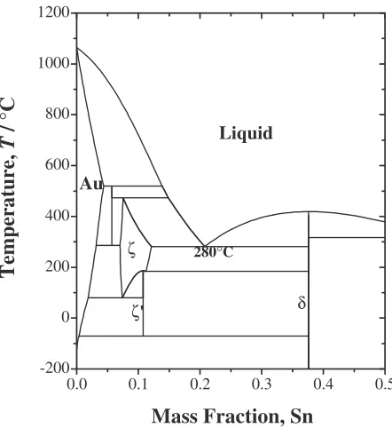
high-tin alloys are available as lead-free solder alloys. However, only a few of the alloys that can replace high-Pb solders have high melting temperatures. One strong candidate is the eutectic 80Au–20Sn solder by weight (71Au–29Sn by molar content); as shown in Fig. 1, this hard solder has an attractive melting point of 280C.3)In addition, the yield strength of
this solder is about the same as the yield strength of Cu. When considering the use of eutectic Au–Sn solder, the first concern is the stress caused by the thermal expansion mismatch. Although the eutectic Au–Sn solder has no fatigue problem because of its hardness, the stresses that develop in typical bonded structures do not incur plastic deformation.
Eutectic Au–Sn solder has been successfully used for highly reliable die attach and fluxless soldering in optoelec-tronic packaging.4,5)This type of solder has high thermal and
electrical conductivity, corrosion resistance, no thermal fatigue and the possibility of fluxless soldering.
Traditionally, a system of Ti/Pt under bump metallurgy (UBM) has been used for eutectic Au–Sn soldering.6,7)In this
case, the interaction between the Pt and Sn creates an excessive buildup of intermetallic compounds (IMCs), such as PtSn and PtSn4.8)Therefore, the Au–Sn ratio in the solder changes to a more Au-rich composition, which significantly increases the liquidus temperature for the Au–Sn alloy. As a result, a nonuniform joint structure is formed, and this structure degrades the performance of the bonded chip.
In view of the degradation, several research efforts have
been attempted to replace the Pt-based UBM. Nickel is an attractive replacement for the diffusion barrier metal because, as the Au–Ni phase diagram suggests, the solubility of Ni in Au is limited at soldering temperatures and Au and Ni fail to dissolve into each other below 100C.9)Moreover, in contrast
to Pt, Ni dissolves into an Sn-based solder at a low rate and it has higher thermal and electrical conductivities than other barrier metals, such as Cr and Pt.10,11) Of course, the difference in thermal conductivity and electrical conductivity between Ni and Cr or Pt may not be important in this application because the layers are thin and the resulting
0.0 0.1 0.2 0.3 0.4 0.5 -200
0 200 400 600 800 1000 1200
280°C
ζ' δ
Au
ζ
Liquid
Temperature,
T
/
°
C
Mass Fraction, Sn
Fig. 1 Au–Sn binary phase diagram.3)
*Corresponding author, E-mail: [email protected]
Special Issue on Lead-Free Soldering in Electronics III
[image:1.595.317.538.372.613.2]difference in thermal resistance and electrical resistance can be ignored. Furthermore, a part of the Ni layer turns in the IMC layer after the soldering process.
Songet al.studied how the Au–Sn solder joint interacts on Cu and later replaced the UBM with a Cu/Ni/Au multi-layer.12,13)Because they used typical electroless Ni plating,
their work involved phosphorus (P). Moreover, they focused on the microstructure of the solder alloy itself rather than on the joint interface.
Our aim is to clarify the microstructural evolution of the eutectic Au–Sn solder’s joint interface. We conducted two kinds of experiments. Firstly, we examined the microstruc-tural evolution of the IMCs between the eutectic Au–Sn and the pure Ni substrate (which contained no phosphorus) with respect to different soldering times and temperatures. Secondly, we studied how the eutectic Au–Sn solder reacted over time with sputtered UBM (Al/Ni(V)/Au) at 300C.
2. Experimental Procedures
The eutectic 80Au–20Sn solder alloys were prepared from Au and Sn metals of purity higher than 99.9 percent. The samples were encapsulated in quartz tubes under vacuum, and then melted and mechanically mixed. We shaped the molten alloy into a wire-type specimen by injecting it through a fine hole (0.5 mm in diameter) and quenching it in water. We then cut the specimen into 1.1 mm lengths and converted it into a spherical shape (750mmin diameter) by dropping it in silicone oil at 320C.
In the first experiment, we put the spherical specimens on a Ni substrate (with a purity higher than 99.9 percent and a thickness of 0.5 mm), after first polishing the substrate with 1mmof diamond paste and cleaning it with an acetone and ethanol solution. We then conducted sessile drop experi-ments in air by using rosin mildly activated flux. Next, we did soldering to isothermally observe the morphological change of the joint interface at 300, 350 and 400C for periods of
1 min up to 32 min, after which we quenched the as-soldered specimens in water at room temperature. Finally, to observe a cross section of the specimen, we cut the middle part and polished it with 0.25mmof diamond paste.
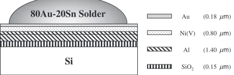
In the second experiment, we used a trilayer of the Al/ Ni(V)/Au structure as the UBM on an Si chip with a 1mm
thick Al metal pad, as shown in Fig. 2. We then sputtered the Al layer with a thickness of 0.4mmand the Ni(V) layer with a thickness of 0.8mm. To coat the top Au layer to a thickness of 0.18mm, we immersed it in the Au coating solution. In addition, the Ni layer contained 7 at%V to reduce the magnetic interference during the sputtering process. Next,
we conducted the sessile drop experiments in silicone oil to ensure temperature homogeneity without having to use rosin mildly activated flux. Finally, we performed the soldering at 300C for periods ranging from 5 s to 5 min.
In both experiments, we examined the cross-sectional microstructure of the solder joint by using a scanning electron microscope (SEM) operated at 10 kV in a back scattered electron detector mode. In addition, to analyze the compo-sition of the IMCs, we used an energy dispersive X-ray (EDX) operated at 20 kV. We found that the spatial resolution was approximately 1mmdiameter near the target point, and we determined the compositions by averaging more than five measurements. Next, to calculate the average thickness of each layer of the IMCs, we divided the area of the layers by the width of the image. Furthermore, to measure the thickness of each layer, we used more than five SEM micrographs and we took into account the protruding particles. The error bars were determined as one standard deviation.
3. Results and Discussion
3.1 Microstructural evolution at the interface of a
eutectic Au–Sn solder joint on a Ni substrate
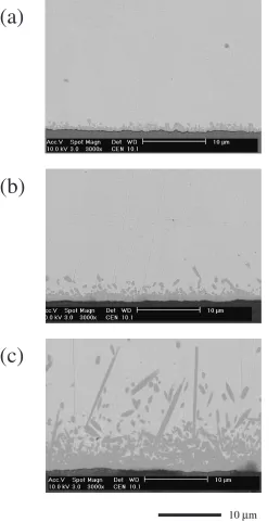
Figures 3 and 4 show typical SEM micrographs of solder joints. Figure 3 shows a eutectic Au–Sn solder on a Ni substrate after soldering at 300C for 1, 8 and 32 min, while
Fig. 4 shows the results of soldering at 400C. The interfacial
IMCs seemed to grow initially as layer-type compounds and then coarsened with prolonged soldering. After a closer look, however, we found that the merged rod-type IMC particles formed a layer. Many IMC particles, which look like islands, were actually cross sections of the rod-type IMC particles grown randomly from different locations on the interface.
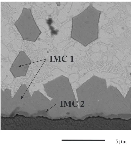
It is difficult to determine the true shape of the IMC particles solely on the basis of the cross-sectional micro-graphs. We tried taking top view micrographs of the solder joint after we had etched away the remaining solder but the etching process was unsuccessful. Nonetheless, as the soldering temperature increased, the morphology generally changed from a long, thin rod-type to a short, thick type. In particular, as seen in Fig. 4(c), the island-type particles in the solder matrix seem to be cross sections of hexagonal cylinders that have been cut at a certain angle, thereby implying that the IMC particles (IMC1 in Fig. 5) take on the shape of a hexagonal cylinder.
As shown in Fig. 5, the microstructure inside the solder is lamellar and, as expected from Fig. 1, it must be composed of AuSn (-phase) and Au5Sn (-phase). The bright constituent in the eutectic microstructure is the-phase, while the darker one is the-phase. After soldering the specimen at 400C for
32 min, we found two types of IMCs, marked IMC1 and IMC2, near the joint interface. To measure their composi-tions, we used EDX (Table 1).
As expected, we identified the bright phase of the lamellar structure as Au5Sn. The IMC1 phase was (Au,Ni)3Sn2 and the IMC2 phase was (Au,Ni)3Sn. According to Fig. 6, the tie line from the liquid eutectic Au–Sn solder composition is directed toward the Ni3Sn2phase, whereas the Ni3Sn phase is located in the middle of the tie line that connects Ni3Sn2 to Si
Si 80Au
80Au--20Sn Solder20Sn Solder Au (0.18
Ni(V) (0.80
Al (1.40
SiO2 (0.15
µ
µ
µ
µm)
m)
m)
m)
[image:2.595.55.285.692.766.2]Ni.14) We suggest, therefore, that the (Au,Ni)
3Sn2 phase is initially formed when the liquid eutectic Au–Sn solder reacts with the Ni substrate, and that the (Au,Ni)3Sn phase is formed when the preformed (Au,Ni)3Sn2 phase reacts with the Ni substrate. This kind of explanation is similar to that of Ronka et al., who used a phase diagram to predict a microstructural evolution of IMCs at the interface of the solder joint.15) On the other hand, Songet al. observed no
(Au,Ni)3Sn phase but only the (Au,Ni)3Sn2 and Au5Sn () phases, which were present probably because of the short reflow time and the low reflow temperature.12,13)The reflow in their study included an exposure of 75 s above 280C, with
[image:3.595.58.542.61.560.2]a peak temperature of 315C.
Figure 7 shows the growth behaviour of IMC1 (excluding IMC2 in Fig. 5). The IMC1 thickness increases with
soldering time, but the soldering temperature has a weaker effect on thickness than the soldering time. The joint interface shows an IMC1 buildup with a similar thickness. As long as the soldering time is the same, the difference in thickness is smaller than 1mm.
The growth of IMCs is unlikely to be controlled by just one mechanism. Commonly, the growth of IMCs is affected by several factors such as soldering temperature, the number of diffusion paths or channels in the IMC layer, and the compositional difference between the solder and the IMCs. In the case of fine-grained intermetallics, grain boundary diffusion is regarded as dominant for the growth of the interfacial layer.
As shown in Figs. 3 and 4, the lateral size of the rod-type intermetallic grains at 300C is much smaller than the grains 10 µm
(a)
(b)
(c)
10 µm
Fig. 3 Back scattered SEM images of cross sections of the eutectic Au–Sn solder on Ni, soldered at 300C for (a) 1 min, (b) 8 min and (c) 32 min.
(a)
(b)
(c)
10 µm
10 µm
[image:3.595.48.306.74.555.2] [image:3.595.341.548.76.556.2]soldered at 400C. Thus, at lower temperatures, many empty
channels exist among the small intermetallic grains, and these channels can accelerate the growth of the intermetal-lics.16)At 400C, the reaction rate is thermally activated but there are fewer diffusion paths or channels because of the grain coarsening effect. As a result, the growth rate of IMCs
is retarded. This retardation probably explains why the thickness of IMC1 is similar even if they are soldered at three different temperatures between 300 and 400C.
Songet al.observed that, for aging at 200C, the growth
rate of the interfacial layer in the eutectic Au–Sn solder bump on Ni is only about half the growth rate of the interfacial layer in the same solder bump on Cu.12,13) Subsequently, we focused on liquid-state soldering of the same alloy at higher temperatures up to 400C, and we observed that the growth in the kinetics of the interfacial IMCs was retarded.
3.2 Microstructural evolution at the interface of a
eutectic Au–Sn solder joint on Al/Ni(V)/Au
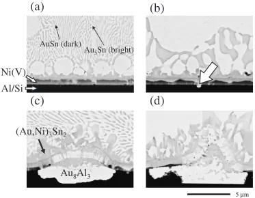
New UBM was used in this test. Figure 8 shows the cross-sectional microstructure of the joint interface after we had soldered the eutectic Au–Sn solder on Al/Ni(V)/Au at 300C
for periods of 20 s to 5 min. As shown in Fig. 5, the bright constituent in the eutectic Au–Sn solder is Au5Sn (-phase) and the dark constituent is AuSn (-phase). Compared with Fig. 5, the large islands of the-phase in Fig. 8(a) seem to have been caused by the Au that dissolved from the thin protective Au layer, which we deposited to ensure wetting by the solder. Once the solder became molten, the Au layer dissolved and slightly increased the Au content in the liquid solder. This process caused the Au–Sn solder to have an off-eutectic composition, and it enabled the prooff-eutectic forma-tion of the -phase. Our results are consistent with the findings of Songet al.13)The only difference was the UBM
structure; that is, in their setup, Song et al. used Cu/ electroless Ni/Au.
After we had soldered for 20 s, the protective Au layer had already dissolved into the solder, and the Ni(V) layer had partially dissolved into the solder. Thus, the shape along the interface was rugged. The Al underlayer was sporadically exposed to the solder, and Au–Ni–Sn particles formed at several locations [Fig. 8(a)]. The lamellar microstructure inside the solder was typical of a eutectic alloy. After we had soldered for 1.5 min, the growth of the intermetallic layer was not uniform. Hence, we detected a locally attacked spot in the
IMC 1
IMC 2
5 µm
5 µm
Fig. 5 Back scattered SEM image of a cross section of the eutectic Au–Sn solder on Ni, soldered at 400C for 32 min. An enlarged image of Fig. 4(c)
[image:4.595.54.285.71.323.2]is shown, at a different interfacial location.
Table 1 Compositions (in at%) of IMCs after soldering at 400C for
32 min.
Au (at%) Ni (at%) Sn (at%) phase formula IMC 1 13.6 (1.1) 47.2 (1.6) 39.2 (0.7) (Au,Ni)3Sn2
IMC 2 2.9 (0.1) 72.5 (0.6) 24.6 (0.7) (Au,Ni)3Sn
bright phase
inside the solder 83.1 (1.0) 16.9 (1.0) Au5Sn
ζ
δ
γ
(Au5Sn) (AuSn)
(Ni3Sn2)
IMC 1
IMC 2
Fig. 6 Isothermal ternary phase diagram of Au–Sn–Ni (at%) at 400C.14)
1 2 3 4 5 6
0 1 2 3 4 5 6 7 8 9
IMC thickness,
t
/
µ
m
Time
1/2,
t
1/2/ min
1/2300°C
Linear fit at 300°C 350°C
Linear fit at 350°C 400°C
Linear fit at 400°C
[image:4.595.313.541.76.260.2] [image:4.595.50.287.405.675.2]Al layer, as marked by an arrow in Fig. 8(b). The spot was probably caused by differences in the Ni content that had dissolved into the molten solder. The eutectic Au–Sn solder that penetrated the Ni(V) layer reached the bottom of the Al layer, and, as shown in Fig. 8(c), some of the Au reacted with Al to form an Au–Al compound. We measured the composition as (70–74)Au(25–29)Al (in atomic percent), and this composition corresponded to the Au8Al3 phase. Moreover, (Au,Ni)3Sn2 formed at the interface of the solder and the Ni(V) layer.
[image:5.595.112.485.75.365.2]When an Au–Al compound forms at the interface, the volume of the compound expands. The (Au,Ni)3Sn2layer is lifted up as a result of the compound’s volume expansion and, as shown in Fig. 8(d), the interlocked (Au,Ni)3Sn2grains are broken and separated at weak points along the interface. Eventually, after we had soldered for 5 min, as shown in Fig. 9, the liquid Au–Sn solder entered through the dis-connected (Au,Ni)3Sn2 layer and filled the area below the (Au,Ni)3Sn2 layer and above the Si chip. The arrow shows the presumed direction of the solder flow. By this stage, the entire UBM reacted to form (Au,Ni)3Sn2or diffused into the solder matrix.
The Au–Al compound forms easily between Au and Al because the activation energy that forms the Au–Al com-pound is smaller than 1 eV.17) To determine the extent to
which the formation of the Au–Al compound changes the volume, consideration was given to the densities of Al, Au and the Al–Au compound.18)The in eq. (1) expresses the volume ratio of vc=vAl, which is equal to the ratio of the
thickness of the Au–Al compound to that of the Al layer, hc=hAl:
¼ vc
vAl
¼ hc
hAl
¼Al
c
1þAAuPAu
AAlPAl
; ð1Þ
wherevis the volume,h is the height,is the density, the subscriptcstands for the Au–Al compound,Aiis the atomic
mass, and Pi is the atomic fraction of i in the Au–Al
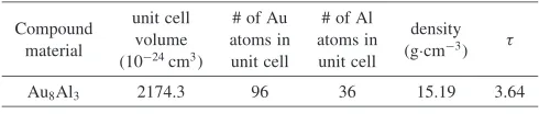
compound (i¼Au, Al). The value of c in Au8Al3 was already calculated using the volume of the unit cell and the number of atoms in the unit cell as given by Range and Buchler.19)By usingcfor Au8Al3andAl, we calculatedAi,
Pi, and.20)
(a)
(d)
(c)
(b)
5 µm
5 µm
Au
8Al
3(Au,Ni)
3Sn
2Ni(V)
Al/Si
Au
5Sn (bright)
AuSn (dark)
Fig. 8 Back scattered SEM images of cross sections of the joint interface between eutectic Au–Sn and Al/Ni(V)/Au soldered at 300C
for (a) 20 s, (b) 1.5 min, (c) 2.5 min and (d) 3 min.
10 µm 10 µm
SiO2/Si
Fig. 9 Back scattered SEM image of the cross section of the joint interface between eutectic Au–Sn and Al/Ni(V)/Au soldered at 300C for 5 min.
[image:5.595.306.547.424.580.2]In Table 2, the value of in Au8Al3 shows that the thickness of the layer increases about 3.6 times more than that of Al. Therefore, when Au8Al3 forms between Au and Al, the volume increases significantly at the joint interface. Because the volume expansion weakens the bond at the joint interface, the joint interface may be separated from the Si chip and a failure may occur in the device. This outcome is of course detrimental, and the Al layer must be protected in a safer way to be used as UBM material. For this purpose, we strongly recommend a Ni(V) layer that is thicker than 0.8mm.
4. Summary
We studied the soldering behaviour of the eutectic 80Au– 20Sn alloy in two types of metallization with respect to the variables of time and temperature. In the case of the Ni substrate, we observed two IMCs at the joint, namely (Au,Ni)3Sn2 and (Au,Ni)3Sn. The (Au,Ni)3Sn2 phase was initially formed by the reaction between the liquid eutectic Au–Sn solder and the Ni substrate; the (Au,Ni)3Sn phase was formed by the reaction of the preformed (Au,Ni)3Sn2 phase and the Ni substrate. As the soldering temperature increased, the morphology of the (Au,Ni)3Sn2 grains changed from a long, thin, rod-like shape to a short, thick shape. The thickness of the IMC layer was similar up to 32 min, even if the soldering was performed at different temperatures between 300 and 400C.
We also investigated how the eutectic Au–Sn solder reacted with the sputtered UBM (Al/Ni(V)/Au) at 300C for
5 min. The protective Au layer dissolved away, and the Ni(V) layer partially dissolved into the solder. Thus, some of the Au reacted with the Al underlayer to form the Au8Al3 com-pound, and the volume of the compound expanded at the joint. The (Au,Ni)3Sn2 layer at the joint was lifted up and some of the interlocked (Au,Ni)3Sn2grains were broken and separated at weak points. As a result, the joint interface separated from the Si chip and failure occurred in the device.
Acknowledgments
This study has been supported by the Center for Electronic Packaging Materials (CEPM) of the Korea Science and Engineering Foundation (KOSEF). We also gratefully ac-knowledge the general help of Mr. Alex J. Chang of Gunn High School, who participated in the early stage of this study as a member of an international internship program at the Korea Advanced Institute of Science and Technology.
REFERENCES
1) F. W. Gayle, G. Becka, J. Badgett, G. Whitten, T.-Y. Pan, A. Grusd, B. Bauer, R. Lathrop, J. Slattery, I. Anderson, J. Foley, A. Gickler, D. Napp, J. Mather and C. Olson: JOM53(2001) 17–21.
2) Lead-free Solder Project Final Report(National Center for Manufac-turing Science, Ann Arbor, 1997).
3) P.-Y. Chevalier: Thermochim. Acta130(1988) 1–13.
4) S. Anhock, H. Oppermann, C. Kallmayer, R. Aschenbrenner, L. Thomas and H. Reichl:22nd Proc. IEEE/CPMT Electron. Manu. Tech. Symp.(1998) pp. 156–165.
5) D. G. Ivey: Micron29(1998) 281–288.
6) A. Katz, K. W. Wang, F. A. Baiocchi, W. C. Dautremont-Smith, E. Lane, H. S. Luftman, R. R. Varma and H. Curnan: Mater. Chem. Phys.
33(1993) 281–288.
7) A. Katz, F. Baiocchi, E. Lane, C. H. Lee, C. Hall, J. Doting, C. Grijsbach and K. Harris: J. Appl. Phys.75(1994) 563–567. 8) C. H. Lee, Y. M. Wong, C. Doherty, K. L. Tai, E. Lane, D. D. Bacon,
F. Baiocchi and A. Katz: J. Appl. Phys.72(1992) 3808–3815. 9) T. B. Massalski:Binary alloy phase diagram, 2nd ed. (ASM
Interna-tional, Material Park, 1990), pp. 402–404.
10) R. J. K. Wassink:Soldering in Electronics, 2nd ed., (Electrochemical Publications Limited, British Isles, 1989) pp. 179–180.
11) R. R. Tummala, E. J. Rymaszewski and A. G. Klopfenstein: Micro-electronics Packaging Handbook, 2nd ed. (Chapman & Hall, New York, 1997), pp. 76–127.
12) H. G. Song, J. W. Morris, Jr. and M. T. McCormack: J. Electron. Mater.
29(2000) 1038–1046.
13) H. G. Song, J. P. Ahn and J. W. Morris, Jr.: J. Electron. Mater.30
(2001) 1083–1087.
14) A. Neumann, A. Kjekshus and E. Rost: J. Solid State Chem.123(1996) 203–207.
15) K. J. Ronka, F. J. J. van Loo and J. K. Kivilahti: Scr. Mater.37(1997) 1575–1581.
16) M. Schaefer, R. A. Fournelle and J. Liang: J. Electron. Mater.27(1998) 1167–1176.
17) G. G. Harman:Wire Bonding in Microelectronics, 2nd ed. (McGraw-Hill, New York, 1997) pp. 116–127.
18) H. Kato: Jpn. J. Appl. Phys.25(1986) 934–935.
19) K.-J. Range and H. Buchler: J. Less-Common Met.154(1989) 251– 260.
20) J. F. Shackelford:Materials Science for Engineers, 3rd ed. (Macmillan, New York, 1992) pp. 738–740.
8 3
and Au.
Compound material
unit cell volume (1024cm3)
# of Au atoms in unit cell
# of Al atoms in unit cell
density (gcm3)
Au8Al3 2174.3 96 36 15.19 3.64
[image:6.595.46.291.94.146.2]