Integration of Dye Lasers and
Microfluidics for Biochemical Analysis
Thesis by
Yan Chen
In Partial Fulfillment of the Requirements for the Degree of
Doctor of Philosophy
California Institute of Technology Pasadena, California
2009
2009
Yan Chen
Acknowledgements
The six years at Caltech have been the most memorable time in my life so far, I owe many thanks for my experience here. First of all, I would like to thank my advisor, Prof. Axel Scherer, for providing me with the opportunity and resources to complete my Ph.D. at Caltech. I am grateful to his guidance and support through all these years. His broad perspective, valuable advice, and sincere mentorship have always been a source of inspiration and motivation.
I would also like to thank my committee members: Prof. Changhuei Yang, Prof. Oskar Painter, Prof. Yu-Chong Tai, and Prof. Chin-Lin Guo, and other members in my candidacy committee: Prof. Mory Gharib, and Prof. Mladen Barbic.
My great thanks go to my collaborators: Dr. Zhenyu Li and Dr. John Zhong. It has been great to work with Dr. Zhenyu Li, I am most grateful for all the helpful discussions and valuable advice from him. Collaboration with Dr. John Zhong in USC Medical School has been very fruitful and enjoyable. I thank him for providing many valuable resources for research, and being a great friend.
Walker, Teresa Emery, Lin Zhu, David Henry, Michael Shearn, Uday Khankhoje, Guangxi Wang, Ting Hong, Jingqing Huang, and Sameer Walavalkar. I would like to thank our secretary, Kate Finigan, and our lab coordinator, Dr. Guy DeRose, who have been working hard to enable an efficient working environment for all of us. I have been extremely fortunate to work with so many wonderful people in my time at Caltech.
Abstract
Contents
Acknowledgements ...iii
Abstract ... v
List of Figures ... x
List of Tables ... xv
Glossary of Acronyms ... xvi
1 Introduction ... 1
1.1 Overview ... 1
1.1.1 Optics in microfluidics ... 1
1.1.2 Biochemistry in microfluidics ... 3
1.2 Thesis organization ... 4
2 Modeling of Circular Grating Structure by Transfer Matrix Method ... 5
2.1 Introduction ... 5
2.1.1 Circular gratings ... 5
2.1.2 Transfer matrix method ... 7
2.2 Transfer matrix analysis ... 8
2.2.1 Maxwell’s equation ... 8
2.2.2 Transfer matrix method ... 11
2.2.3 Transfer matrix method coefficients ... 14
2.3 Simulation results ... 17
2.3.1 Index matching ... 17
2.3.3 Electromagnetic field plot ... 23
3 Nanoimprinted Circular Grating Dye Laser ... 25
3.1 Introduction ... 25
3.2 Materials ... 28
3.2.1 PMMA ... 28
3.2.2 Organic dye ... 28
3.2.3 Cytop ... 29
3.3 Laser cavity design ... 30
3.4 Fabrication process ... 31
3.4.1 Imprint mold fabrication ... 31
3.4.2 Laser chip fabrication ... 34
3.4.3 Nanoimprint process ... 35
3.5 Results and discussion ... 38
3.6 Summary ... 42
4 Optofluidic Circular Grating Dye Laser ... 43
4.1 Introduction ... 43
4.2 Materials ... 46
4.2.1 PDMS ... 46
4.2.2 PFPE ... 47
4.2.3 Laser dye and solvents ... 49
4.3 Laser cavity design ... 51
4.3.1 Circular grating distributed feedback structure ... 51
4.3.2 Flow channel design ... 53
4.4 Fabrication process ... 55
4.4.1 Mold fabrication ... 55
4.4.2 Laser chip fabrication ... 59
4.5 Results and discussion ... 62
5 Microfluidic Device as a Platform for Single Cell
Biochemical Analysis ... 66
5.1 Introduction ... 66
5.1.1 Microfluidic device as a platform for biochemical analysis ... 66
5.1.2 Significance of single-cell gene analysis ... 67
5.2 Design of microfluidic devices for single-cell analysis ... 69
5.2.1 First generation of microfluidic chip ... 69
5.2.2 Second generation of microfluidic chip ... 70
5.3 Materials and methods ... 72
5.3.1 Mold fabrication ... 72
5.3.2 Device fabrication ... 72
5.3.3 Microfluidic station ... 73
5.3.4 Synthesis of cDNA from hESCs... 74
5.4 Operation of microfluidic device ... 75
5.5 Results and discussion ... 77
5.5.1 Device efficiency ... 77
5.5.2 Gene expression of single hESC cells ... 80
5.6 Conclusions ... 82
6 Summary ... 85
Appendix A ... 87
Appendix B ... 90
List of Figures
2.1 Diagram of a circular grating resonator design. The scheme illustrates the second-order Bragg diffraction including (1) normal diffraction to the grating surface
(first-order) and (2) in-plane feedback (second-order) ... 6
2.2 Schematic representation of a circular grating, with grating period , duty cycle w/ dc , effective indices nI and nII, cavity radius r1,r2,,rN1 ... 11
2.3 Effective index approximation of solid-state dye laser ... 28
2.4 Effective index approximation of optofluidic dye laser ... 17
2.5 The power ratio in circular grating with period of 440 nm for m=0,1,2 ... 19
2.6 The power ratio in circular grating with period varying from 400 nm to 450 nm ... 20
2.7 The power ratio in circular grating with two groove depths ... 21
2.8 The power ratio in circular grating with period varying from 400 nm to 440 nm ... 22
2.9 The 1-D graph of the normalized jm z H , field in circular grating for m=0,1 ... 23
3.1 The general nanoimprint process... 26
3.2 Schematic diagram of a nanoimprinted circular grating dye laser chip ... 27
3.3 The monomer building block of PMMA ... 28
3.4 Rhodamine 640 molecule structure ... 29
3.5 Cytop molecule structure ... 29
3.6 General design of a circular grating distributed feedback structure ... 30
3.7 The SEM image of the cross section of an etched SiO2 grating ... 31
3.8 Schematic fabrication procedure for the circular grating nanoimprint hard mold. (a) The original wafer with 500 nm SiO2 on top of silicon substrate. (b) PMMA is spun on the sample for subsequent e-beam lithography steps. (c) The PMMA is exposed by b-beam, and the circular grating pattern is completely transferred into PMMA after developing the exposed resist. (d) The pattern is transferred into the SiO2 via CHF3 RIE etch, and the PMMA residue is removed after dry etch ... 32
3.9 SEM images of (a) the top view and (b) the angled view of SiO2 mold ... 33
3.10 Summary of the Cytop and PMMA substrate preparation process ... 35
3.11 Schematic nanoimprint process of circular grating polymer dye laser ... 36
3.13 Measurement setup for polymer dye laser device ... 38
3.14 Nanoimprinted circular grating DFB dye laser spectrum. The measured linewidth is 0.18 nm. Inset: Polymer laser chip excited by Nd:YAG 532nm laser pulse ... 39
3.15 The output laser power vs. the absorbed pump energy curve. The threshold pump fluence is 1.31 μJ/mm2 ... 40
3.16 (a) Far-field image of the emission pattern recorded by a CCD camera. (b) Circular grating DFB laser far-field radiation patterns through a linear polarizer with different orientation angles ... 41
4.1 Schematic diagram of an optofluidic circular grating dye laser chip ... 45
4.2 Rhodamine 6G molecule structure ... 49
4.3 Cross sections of stimulated singlet state absorption and emission for Rhodamine 6G in ethanol ... 49
4.4 General design of an optofluidic circular grating DFB dye laser cavity ... 51
4.5 Illustration of the Bragg diffraction in the second-order circular grating. First-order Bragg reflection induces coupling to vertical propagating waves, and second-order Bragg reflection leads to in-plane feedback ... 52
4.6 PDMS microvalves (push-down version). Source: www.fluidigm.com ... 53
4.8 Schematic fabrication procedure for the circular grating hard mold. (a) The original wafer with 1 µm SiO2 on top of silicon substrate. (b) Cr is evaporated on the sample. (c) PMMA is spun on top of the Cr for subsequent e-beam lithography steps. (d) The PMMA is exposed by e-beam, and the circular grating pattern is completely transferred into PMMA after developing the exposed resist. (e) The Cr underneath the exposed pattern is removed by wet etch, and the remaining PMMA is also
removed. (f) The pattern is transferred into the SiO2 via DRIE etch ... 56
4.9 The SEM images of the cross-section of etched SiO2 gratings. (a) A cut-away view of the gratings. (b) Deeply etched trenches in the circular grating structure ... 57
4.10 SEM images of (a) the top view and (b) the angled view of the SiO2 mold ... 58
4.11 Fabrication process of hybrid PFPE/PDMS laser chip ... 60
4.12 (a) SEM images of SiO2 mold. (b) ESEM images of PFPE replica ... 61
4.13 Measurement setup of optofluidic dye laser chip ... 62
4.14 Optofluidic circular grating DFB dye laser spectrum. Inset: The output laser power vs. the pump energy curve ... 63
5.1 20X single-cell mRNA extraction microfluidic device filled with food dye ... 69
5.2 32X single-cell gene profiling microfluidic device filled with food dye ... 71
5.4 Merged image of immunofluorescent-stained (Oct-3/4) and light microscope images from a pluripotent hESC colony ... 74
5.5 The process flow in the single-cell microfluidic processor ... 76
5.6 Measuring absolute molecule numbers of three genes in single hESC with multiplex quantitative PCR ... 79
List of Tables
4.1 Refractive indices of PDMS-compatible solvents ... 50
Glossary of acronyms
2D – Two-dimensional
DBR – Distributed Bragg reflector
DFB – Distributed feedback
ESEM – Environmental scanning electron microscope
FDTD – Finite difference time domain
FP – Fabry-Perot
FWHM – Full width at half maximum
MIBK – Methyl isobutyl ketone
OSA – Optical spectrum analyzer
PL – Photoluminescence
RIE – Reactive ion etching
PMMA – Poly(methyl methacrylate)
Q – Quality factor
Chapter 1
Introduction
1.1
Overview
1.1.1
Optics in microfluidics
The field of microfluidics continues to become an important area with novel applications in biotechnology [1]. The most important goal for microfluidics is to achieve a complete “lab-on-a-chip” system, which is capable of performing biological and chemical experiments normally carried out in a standard full-size laboratory. While efforts are made to develop the microfluidic system to realize more functionality for various biochemical reactions, the integration of optical components into microfluidic systems becomes more and more indispensable.
We are very interested in the miniaturization and integration of dye lasers into microfluidic systems because of their broadband tunablity, low cost, and easy fabrication. Dye lasers have been widely used as tunable, coherent light sources for spectroscopic analysis in the visible wavelength region (from 400 nm to 900 nm) during the past 30 years [3]. Miniaturized dye lasers, which can be integrated in lab-on-a-chip microsystems, would similarly have numerous applications. For applications in biochemical analysis in microfluidic systems, a surface emitting laser is more useful than other lasers because of its stacked substrate structure. Therefore, we choose a circular grating structure as the laser resonator design to produce low-threshold surface emitting lasing. The laser operating characteristics can be significantly improved by the two-dimensional nature of the resonator structure.
Two types of miniaturized dye lasers with the circular grating geometry are demonstrated in this thesis: solid-state and optofluidic dye lasers. For the solid-state dye laser, the laser dye is doped in the polymer forming the laser resonator, and it is fabricated using nanoimprint lithography. For the microfluidic dye laser, the laser dye is dissolved in an organic solvent and flowed through a microfluidic channel with laser resonator embedded, and it is realized by soft lithography. They can produce high-intensity and narrow-linewidth lasing with a well-defined output beam.
1.1.2
Biochemistry in microfluidics
As we study the optical integration in microfluidic systems towards fully functional “lab-on-a-chip” system, we are exploring more capabilities of the microfluidic system in the field of biochemical analysis. Lab-on-a-chip devices have the potential to revolutionize biochemistry by allowing complicated biochemical procedures to be performed on a small microfluidic chip. Single-cell processing is one of the major applications of microfluidics that can take advantage of its nanoliter fluid handing abilities.
A microfluidic approach that can extract gene expression information from individual single cells is described in this thesis. The integrated process: cell capture/lysis, mRNA isolation/purification, and cDNA synthesis/purification for single human embryonic stem cells is implemented on a microfluidic device. With the improved design of the microfluidic circuit, a parallel processing of dozens of cells with 100% efficiency can be achieved.
between measurements from population cDNA and single-cell cDNA. The results underscore the importance of discrete single-cell analysis, and the advantages of a microfluidic approach in stem-cell gene expression studies.
1.2
Thesis organization
The thesis is organized as follows: Chapter 2, Chapter 3 and Chapter 4 focus on the optics integration of the microfluidic system, and Chapter 5 highlights the biochemistry aspect of the microfluidic system.
Chapter 2
Modeling of circular grating structure by
transfer matrix method
2.1
Introduction
2.1.1
Circular grating
Laser (Light Amplification by Stimulated Emission of Radiation) is composed of a gain
medium and a resonant optical cavity [4]. The gain medium amplifies the beam by stimulated emission, and the resonant cavity provides the feedback necessary for the lasing operation. For our solid-state and optofluidic dye lasers in Chapter 3 and Chapter 4, we choose the circular grating resonator as laser cavities for their unique two-dimensional nature and enhanced lasing performance.
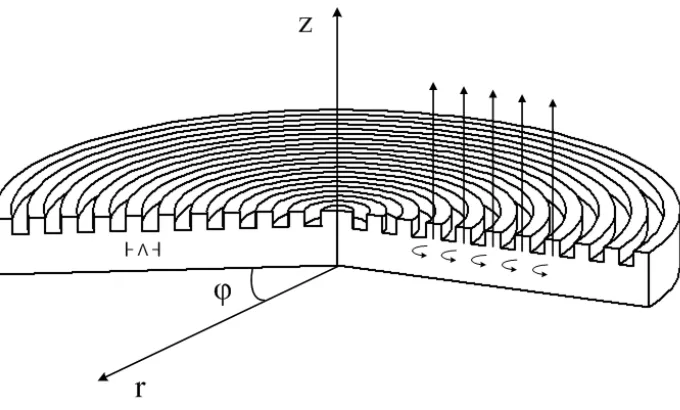
In particular, we use the second-order circular grating distributed feedback (DFB) structure as the resonant cavity. The distributed feedback scheme indicates that the gain material is directly implemented in the grating structure. The circular grating DFB structure satisfies the second-order Bragg condition, Bragg neff, where Bragg is the emission
wavelength, neff is the effective index of the waveguide mode, and is the grating
Figure 2.1: Diagram of a circular grating resonator design. The scheme illustrates the second-order Bragg diffraction including (1) normal diffraction to the grating surface
(first-order) and (2) in-plane feedback (second-order).
2.1.2
Transfer matrix method
To understand the resonant behavior of the circular grating, a theoretical analysis is necessary. There are many methods for modeling circular optical resonators. Most of the models are based on couple mode theory [5-9], which is more suitable for analyzing circular grating structure with shallow trenches and a modest light confinement. In this chapter, we present a transfer matrix method for analyzing circular grating structure with deep etched trenches. The deeper trenches of the structure lead to stronger in-plane effective index modulation, therefore the resonator can confine light in a smaller volume.
The transfer matrix method [10] is a straightforward method for analyzing optical structures composed of an arbitrary number of dielectric layers. When the dielectric properties are taken into account and the boundary conditions are satisfied, a transfer matrix can relate the electromagnetic field on either side of an optical region. Therefore, a complex structure can be modeled by simple matrix multiplication of basic subcomponents. The transfer matrix method is suitable to analysis of various resonant optical cavities, such as multi-section Fabry-Perot, DBR, DFB, and VCSEL geometries [11]. For our application, we are interested in utilizing transfer matrix method for the analysis of structures with cylindrical symmetry.
2.2
Transfer matrix analysis
2.2.1
Maxwell’s equation
To solve the wave equation, we define E and H as the vector electric and magnetic
fields in the circular grating structure, and they are represented by (Ez,Er,E) and
) , ,
(Hz Hr H in cylindrical coordinates. In our 2-D model, we simplify the circular Bragg
grating to infinite cylinders, and consider the system invariant in the z direction. Therefore,
the electrical field and magnetic field can be expressed as i t
e r
E( ,) and H(r,)eit.
The Maxwell’s equation is given below in its differential form
0 0 H E E i H H i E (2.1)
where and are the magnetic permeability and dielectric permittivity in the grating
structure, and is the angular frequency of the electromagnetic field.
At all layer interfaces, the tangential components of the electric and magnetic field E
and H must be continuous. The system is invariant in z direction, therefore the solutions
We can derive the Helmholtz equation from Maxwell’s equation and solve it for the cylindrical coordinate.
2 2
0 H E k (2.2)
where k is the wavenumber in the grating structure and satisfies k2 2.
Expressing the Helmholtz equation in cylindrical coordinates, we have
0 1 ) ( 1 2 2 2 2 2 2 H E k z r r r r r
. (2.3)
Because the system is invariant along the z coordinate, the separation in z components and
in a transversal part is possible. Let 2 2 2 z
T k
k
k , where kT and kz represent the
component for the polar and z coordinates, respectively.
If we apply the following variable separation to Eq. (2.3),
) ( ) ( ) , ( ) ( ) ( ) , ( r R B r H r R A r E z z (2.4)
the equation becomes
0 ) ( ) ( ) ( ) ( ) ( 1 ) ( ) ( ) ( 2 2 2 2 2 2
R r kT
r r R r r R r r r R
. (2.5)
The equation can be separated into two parts with only dependence on r and , and
each part can be solved on its own.
2 2 2 2 2 2 2
2 ( )
) ( 1 ) ( ) ( ) ( )
( r r k m
r R r R r r r R r R r T
The solution of ( ) 2 ( ) 0 2 2
m is either
im e l m m l m m ) ( ) ( ), sin( ) ( ), cos( ) ( 2
1 . (2.7)
The equation below is known as the Bessel differential equation
0 ) ( ) ( ) ( ) ( ) ( 2 2 2 2 2 2 m k r r r R r R r r r R r R r
T . (2.8)
Therefore, the general solution of the time harmonic electromagnetic field is the Hankel function, which is a linear combination of Bessel and the Neumann function,
) ( ) ( ) ( ) ( ) ( ) ( ) 2 ( ) 1 ( r iN r J r r iN r J r m m m m m m (2.9) ) 1 ( m
and (2) m
are the first-kind and second-kind Hankel functions, respectively, m is
the azimuthal order, Jm is the Bessel function, and Nm is the Neumann function.
The solutions of variable separated equations can be inserted into Eq. (2.4),
for the TE mode,
0 ) 2 ( ) 1 ( )] ( ) ( [ ) , ( m im m m m m j
z r r r e
H . (2.10)
for the TM mode,
0 ) 2 ( ) 1 ( ( ) ( )] [ ) , ( m im m m m m j
z r r r e
2.2.2
Transfer matrix method
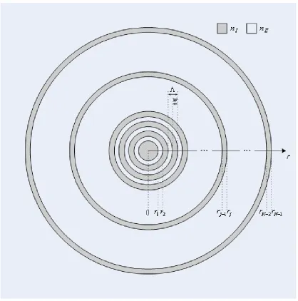
The schematic circular grating laser structure is shown in Fig. 2.2. The circular grating structure consists of N infinite cylindrical concentric layers. Each layer consists of
[image:27.612.116.534.200.622.2]alternating dielectric materials with refractive indices nI and nII.
Our goal is to describe the field propagating in a cylindrical waveguide structure shown in Fig. 2.2. Due to the 2-D nature of the problem, the field solutions can be decomposed into TE and TM polarizations, for which the field in the plane is entirely characterized by (Hz,Er,E)and )(Ez,Hr,H , respectively. The present cylindrical
geometry suggests we expand the fields using first-kind and second-kind Hankel functions,
) 1 ( m
and (2)
m
, which are linearly independent and represent the inward and outward
propagating circular (Hankel) waves.
We are mainly considering the TE polarization, since the perpendicular pumping light on the grating surface will cause almost pure excitation of TE waves [23]. As described in the previous chapter, the general TE solutions of the Maxwell’s equations in each layer j
can be expressed as a linear combination of im j
m (n k0r)e )
1 (
and im
j m (n k0r)e
) 2 (
for
each mode m0,1,,, nj is the effective refractive index in each layer j.
The H-field is expressed as
0 , 0 0 ) 2 ( 0 ) 1 ( ) ( )] ( ) ( [ ) , ( m im m j z m im j m j m j m j m j z e r H e r k n r k n r H . (2.12)
Based on Maxwell’s equations, H njiE
2 0 , j j r j j z j z j z E E i n r H H H r z 0 / / 0 0 0 / / / 2
0 (2.13)
0 , 0 0 ) 2 ( 0 ) 1 ( 0 ) ( )] ( ) ( [ ) , ( m im m j m im j m j m j m j m j j e r E e r k n r k n c n i r E . (2.15)
) 1 ( m
and (2) m
are the derivative of (1) m
and (2) m
, respectively.
Similarly, for TM polarization, the E-field is expressed as
0 , 0 0 ) 2 ( 0 ) 1 ( ) ( )] ( ) ( [ ) , ( m im m j z m im j m j m j m j m j z e r E e r k n r k n r E . (2.16)
Based on Maxwell’s equations, E 0iH,
j j r j z j z j z H H i r E E E r z 0 / / 0 0 0 / / /
0 (2.17)
0 , 0 0 ) 2 ( 0 ) 1 ( 0 ) ( )] ( ) ( [ 1 ) , ( m im m j r m im j m j m j m j m j r e r H me r k n r k n r H (2.18)
0 , 0 0 ) 2 ( 0 ) 1 ( 0 ) ( )] ( ) ( [ ) , ( m im m j m im j m j m j m j m j j e r H e r k n r k n ic n r H 2.2.3
Transfer matrix method coefficients
At the interface between the th
j and (j1)th layers, located at rrj, the tangential
fields components (Ez,H for TM polarization; Hz,E for TE polarization) must be
continuous. The coefficients calculations of Transfer Matrix below are based on TE polarizations. ) , ( ) , ( ) , ( ) , ( 1 1 j j z j j z j j z j j z r H r H r E r E (2.20)
The relationship between the coefficients ( , j)
m j
m
, ( 1, j1)
m j
m
can be expressed by
j m j m j m j m j m j m j m j m a b b a 1 1 (2.21)
where j m j
m b
a , are the complex conjugates of amj,bmj.
( ) ( ) ( ) ( )
1 ) ( ) ( ) ( ) ( 1 0 ) 2 ( 0 1 ) 2 ( 0 1 ) 2 ( 0 ) 2 ( 0 ) 1 ( 0 1 ) 2 ( 0 1 ) 2 ( 0 ) 1 ( k r n k r n k r n k r n D b k r n k r n k r n k r n D a j j m j j m j j m j j m j m j m j j m j j m j j m j j m j m j m (2.22)with the index ratio
j j
n n 1
, ) ( ) ( ) ( )
( (1) 1 0
0 1 ) 2 ( 0 1 ) 2 ( 0 1 ) 1 ( k r n k r n k r n k r n
Dmj m j j m j j m j j m j j . (2.23)
For TM polarization, the only difference is the index ratio
We can obtain an overall transfer matrix relating the inner cavity to the outmost ring by multiplying the transfer matrices for each layer. For j1,2,,N1,
1 1 m m N m N m N m T
. (2.24)
The overall transfer matrix N m
T takes the form
11 11 11 11
m m m m N m N m N m N m N m N m N m N m N m a b b a a b b a A B B A
T (2.25)
with
1 0 0 1 1 1 1 1 1 m m m m m A B B A
T . (2.26)
In order to find resonant modes, we can assume 1 1 m
m
, since every incoming
wave can be considered as an outgoing one after crossing the z axis. The power in each
layer j can be defined as Pmj mj 2 mj 2.
Therefore the ratio of the electromagnetic power confined in the center ring 1 m
P to
that in the outmost ring N m
P is
2 2 2 1 2 1 1 N m N m m m N m m m P P R
(2.27)
1 1 1 1 1 1 ) ( ) ( m N m N m m N m m N m N m m N m N m m N m m N m N m B A A B B A B A
(2.28)
with N
m N m N
m
2 , N
m N m N
m
2 2 1 2 2 1 2 2 N m N m m N m N m m N m N
m A B A B
. (2.29)
So the Power ratio Rm between the center ring and the outmost ring can be expressed
as the function of the wavelength by transfer matrix elements N m
A and N m B , 2 1 N m N m m B A R
. (2.30)
The power ratio can give us an estimation of the resonance peak of the cavity modes in the absence of any source input, which helps us to have a good understanding of the energy confinement in our circular grating structures.
We can also estimate the field in the microcavity with the assumption 1 1 m m , 1 1 j m j m j m j m j m j m A B B A j m j m j m j m j m j m j m A B B A
. (2.31)
Therefore, in the TE polarization, we can write the H-field as a function of N m
A and BmN
( ) ( )
Re 2 ) ( ) ( ) ( ) ( ) ( 0 ) 1 ( 0 ) 2 ( 0 ) 1 ( 0 ) 2 ( 0 ) 1 ( , r k n B A r k n r k n r k n r k n r H j m j m j m j m j m j m j m j m j m j m j m m j z . (2.32)
Similarly, in the TM polarization, we can express the E-field as
( ) ( )
Re 2 )
( (1) 0
, r k n B A r
2.3
Simulation results
2.3.1
Index Matching
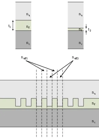
In order to introduce the finite vertical component of the waveguide grating into our transfer matrix formalism, we use the effective index approach. In this method, two characteristic cross sections, the groove and the tooth, form two different slab waveguides, providing effective indices nI and nII for the corresponding layers in our transfer matrix
model.
The effective index approximation for the solid-state circular grating dye laser model is illustrated in Fig. 2.3. The laser waveguide consists of the top cladding (air), the dye-doped polymer film (PMMA), and the lower cladding (Cytop), with the refractive indices of na 1.0, nf 1.49, 34nc 1. , respectively. The variance between neff1 and
2 eff
[image:33.612.242.406.409.641.2]n is caused by the different thickness of polymer film in the groove and the tooth.
In the solid-state circular grating laser structure, the core thickness (the polymer thickness) is 1 um, and the grating trench depth is 400 nm, which gives the thickness of the two slab waveguides as t1 1m and t2 600nm. We can calculate the effective index
using the 1-D multilayer waveguide solver [14]. The effective index of the tooth section is 4791
. 1
1 eff
n , and the effective index of the groove section is neff2 1.3403.
Similarly, the effective index approximation for the optofluidic circular grating dye laser model is illustrated in Fig. 2.4. The laser waveguide consists of the top cladding (PDMS), the liquid gain medium (dye solution), and the lower cladding (PFPE), with a refractive index of nt 1.40, 54nd 1. , 34nl 1. , respectively. The thickness of the
two slab waveguides can be assumed as t1 1.6 m and t2 1 m. The resulting
effective index of the tooth section is neff1 1.5321, and the effective index of the groove
[image:34.612.244.405.412.650.2]section is neff2 1.4007.
2.3.2
Cavity resonance
600 605 610 615 620 625 630 635 640 645 650
10-1 100 101 102
Wavelength []
P
o
w
e
r R
a
ti
o
[a
rb
. u
n
it
s
]
[image:35.612.126.496.173.471.2]m=1 m=0 m=2
Figure 2.5: The power ratio in circular grating with period of 440 nm for m=0,1,2.
For the solid-state dye laser, the corresponding parameters are introduced to the transfer matrix method. We first choose the grating period to be 440, and the duty cycle to be 0.5.
The effective indices are nI 1.48 and nII 1.34, respectively. The overall diameter of
grating is 200 µm, which gives the grating layer number N 250. In Fig. 2.5, we plot the
power ratio between the center ring and the outmost ring for different modes m0, 1, 2.
550 560 570 580 590 600 610 620 630 640 650 10-1
100 101 102
Wavelength []
P
o
w
e
r R
a
ti
o
[a
rb
. u
n
it
s
]
=400
=410
=420
=430
=440
[image:36.612.125.522.141.431.2]=450
Figure 2.6: The power ratio in circular grating with period varying from 400 nm to 450 nm.
Fig. 2.6 shows the resonance peak corresponding to circular gratings with period from 400 nm to 460 nm. From the simulation results we can see that the cavity resonant modes fulfill the second-order Bragg condition Bragg neff. The resonant peak for grating with
580 590 600 610 620 630 640 10-1
100 101 102
Wavelength []
P
o
w
e
r R
a
ti
o
[a
rb
. u
n
it
s
]
[image:37.612.129.496.102.397.2]600nm depth 400nm depth
Figure 2.7: The power ratio in circular grating with two groove depths.
For the optofluidic dye laser, the main different grating parameters are their effective refractive indices. Due to the liquid configuration in fluidic dye laser, it is difficult to retrieve the exact waveguide thickness; here we assume the channel height is 1.6 µm. With a 400 nm groove depth, we obtain nI 1.53 and nII 1.43, if the depth increases to 600
nm, then we have nI 1.53 and nII 1.40. In Fig. 2.7, we compare the power ratio for
570 580 590 600 610 620 630 640 650 10-1
100 101 102
Wavelength []
P
o
w
e
r R
a
ti
o
[a
rb
. u
n
it
s
]
=400
=410
=420
=430
[image:38.612.129.498.139.432.2]=440
Figure 2.8: The power ratio in circular grating with period varying from 400 nm to 440 nm.
Fig. 2.8 shows a series of resonance in the circular grating with period varying from 400 nm to 440 nm for m=1. The effective refractive indices are nI 1.53 and nII 1.40,
respectively. The duty cycle is 0.5, and the grating layer number is N 250. The resonant
2.3.3
Electromagnetic field plot
0 1 2 3 4 5 6 7 8
0 1 2 3 4
Radius []
|Hz
|
2 (m
=
0
)
0 1 2 3 4 5 6 7 8
0 0.5 1 1.5
Radius []
|Hz
|
2 (m
=
1
)
Figure 2.9: The 1-D graph of the normalized jm z
[image:39.612.174.466.138.371.2]H , field in circular grating for m=0,1.
Figure 2.10: The 3-D graph of the normalized jm z
We can have a better understanding of the electromagnetic field in the circular grating by
plotting the normalized jm z
H , field expressed by Eq. (2.32) for m=0 and m=1. Fig. 2.9
plots the 1-D graph of the jm z
H , field, and Fig. 2.10 plots the 3-D graph of the Hzjm
, field.
Chapter 3
Nanoimprinted circular grating dye laser
3.1
Introduction
Within recent years the development of polymer dye lasers has progressed to higher levels of performance and functionality. The most attractive advantages of polymer dye lasers include low-cost processing, wide choice of emission wavelengths, and easy fabrication on flexible substrates. Several waveguide dye lasers have been studied with emission wavelengths ranging from ultraviolet to near infrared [15]. By simply changing the fluorophore doped in the polymer, these lasers can be used as the tunable sources for various applications, including spectroscopy [16].
Figure 3.1: The general nanoimprint process.
For better geometric control, we choose nanoimprint lithography [20] as a direct patterning method. A hard mold is used to transfer patterns with high fidelity into target polymers, and this technique has become an attractive approach to define nanofabricated optical resonator structures. Conjugated polymer lasers fabricated by hot embossing have been studied by Lawrence et al. [21], and 1-D DFB lasers based on organic oligomers using a room temperature nanoimprint method were reported by Pisignano et al. [22, 23].
Figure 3.2: Schematic diagram of a nanoimprinted circular grating dye laser chip.
3.2
Materials
3.2.1
PMMA
PMMA (poly(methylmethacrylate)) is a well-known highly transparent thermoplast. In our laser device, we chose PMMA to be the dye host matrix as well as the nanoimprint material. PMMA was selected as the polymer matrix because of its solubility of the dye molecules, as well as its low absorption at the wavelength for activating the dye molecule. Using PMMA in nanoimprint lithography is very common due to its good mold release properties and small shrinkage under large changes of temperature and pressure [24]. The building block for PMMA is shown in Fig. 3.3.
Figure 3.3: The monomer building block of PMMA.
3.2.2
Organic dye
Figure 3.4: Rhodamine 640 molecule structure.
3.2.3
Cytop
Cytop is a low refractive index perfluoropolymer; its molecular structure is shown in Fig. 3.5. This cyclic fluoro-polymer, poly(1,1,2,4,4,5,5,6,7,7-decafluoro-3-oxa-1,6-heptadiene) is made by Asahi chemicals and used in the electronics industry. It is a hard but amorphous material with Tg ~ 1080 °C. We chose Cytop as a cladding material because of its low refractive index (n=1.34). The material system of PMMA and Cytop has previously been used for commercial polymer optical fibers and simple waveguides [25].
3.3
Laser cavity design
Figure 3.6: General design of a circular grating distributed feedback structure.
The circular grating structure proposed [6] and demonstrated [26] by Erdogan and Hall provides a natural 2-D extension of the basic DFB structure. It allows feedback to be applied in all in-plane directions, and the second-order grating couples the emitted radiation perpendicularly out of the surface of the sample. Fig. 3.6 shows a general design of a circular grating distributed feedback structure. A theoretical analysis of circular grating lasers is described in detail elsewhere [7-9, 27, 28] predicting that only the radial propagating components define the modes in the circularly symmetric grating.
3.4
Fabrication process
3.4.1
Imprint mold fabrication
In our experiments, silicon dioxide (SiO2) was used as the mold material. The grating pattern was defined by electron beam lithography on a LEICA EBPG 5000+ e-beam writer. 8% 495K PMMA was spun on a SiO2 substrate for 1 min at 4500 rpm and baked for 15 min at 170 °C, which formed a 400 nm thick resist layer. The PMMA was exposed by electron beam at 100 keV and 800 μC/cm2 with proximity correction. Development of patterned PMMA film was carried out in a 1:3 MIBK:IPA (methyl isobutyl ketone and isopropanol alcohol) solution for 1 min. The pattern was subsequently transferred from PMMA into SiO2 substrate via reactive ion etching (RIE) using fluorine chemistry (CHF3). The condition of RIE was 20 sccm, 60 mTorr of CHF3 at 110 W for 15 min. Finally the PMMA residue was removed by sonicating the wafer in Chloroform for 2 min. The SiO2 etching rate in the CHF3 RIE process is 30 to 35 nm per min. Fig. 3.7 is the SEM image of the cross section of an etched SiO2 grating with the etched depth of 400 nm. The schematic fabrication procedure for the nanoimprint hard mold is illustrated in Fig. 3.8.
Figure 3.8: Schematic fabrication procedure for the circular grating nanoimprint hard mold. (a) The original wafer with 500 nm SiO2 on top of silicon substrate. (b) PMMA is spun on the sample for subsequent e-beam lithography steps. (c) The PMMA is exposed by e-beam,
and the circular grating pattern is completely transferred into PMMA after developing the exposed resist. (d) The pattern is transferred into the SiO2 via CHF3 RIE etch, and the
The SEM images of both the top view and the angled view of an etched SiO2 mold of circular grating are shown in Fig. 3.9. The grating period is 440 nm, with a center defect of 440 nm and an overall diameter of 200 µm. The trench depth is 400 nm.
Figure 3.9: SEM images of (a) the top view and (b) the angled view of SiO2 mold.
(a)
3.4.2
Laser chip fabrication
The laser chip consists of three layers, the substrate, the cladding, and the polymer matrix. PMMA was selected as the polymer matrix because of the solubility of the dye in PMMA, as well as its low optical absorption within the wavelength range for activating the dye molecules, and its excellent properties for nanoimprint lithography.
To construct the dye laser, a glass substrate (SiO2) was spin-coated with Cytop, a low-refractive-index material (n=1.34) as the lower cladding to ensure the vertical optical confinement. After an oxygen plasma treatment to improve the adhesion of Cytop to the PMMA, dye-doped PMMA (n=1.49) was spun on top of the Cytop layer to serve as the gain medium.
The Cytop and PMMA preparation process for the nanoimprint process is summarized in Fig. 3.10. We began the fabrication process by depositing a 5 µm thick layer of Cytop (CTL-809M, Asahi Glass) on a silicon dioxide substrate. The deposition of the Cytop was accomplished via a series of spinning and thermal curing steps to ensure flatness and uniformity over the wafer. First, we spun the Cytop on the substrate at 1500 rpm (adhesion promoters were not necessary). Next, the Cytop was baked at 65 °C for 60 s, 95 °C for 60 s, and 180 °C for 20 min. The ramping of the bake temperature was critical in attaining flat and uniform surfaces. The spinning and baking steps were then repeated two more times, with a final bake at 180 °C for 3 hours. After the chip cooled down, an oxygen plasma treatment (Anatech SP100) of the Cytop was necessary for the adhesion of Cytop to PMMA. We exposed the oxygen plasma to Cytop at an RF power of 80 W and O2 pressure of 200 mTorr for 30 s.
improved the adhesion between the Cytop and PMMA. Then the substrate was ready for the nanoimprint process to define the laser cavity structure.
Figure 3.10: Summary of the Cytop and PMMA substrate preparation process.
3.4.3
Nanoimprint process
Figure 3.11: Schematic nanoimprint process of circular grating polymer dye laser.
Figure 3.12: SEM images of (a) the SiO2 mold and (b) the imprinted PMMA film.
3.5
Results and discussion
Figure 3.13: Measurement setup for polymer dye laser device.
590 595 600 605 610 615 620 625 630 635 0
0.1 0.2 0.3 0.4 0.5 0.6 0.7 0.8 0.9 1
Wavelength (nm)
N
o
rm
a
li
z
e
d
I
n
te
n
s
it
y
(
a
.u
.)
[image:55.612.139.498.141.425.2]FWHM=0.18nm
Figure 3.14: Nanoimprinted circular grating DFB dye laser spectrum. The measured linewidth is 0.18 nm. Inset: Polymer laser chip excited by Nd:YAG 532 nm laser pulse.
A typical single-frequency lasing spectrum is shown in Fig. 3.14. The lasing wavelength is 618.52 nm, and the measured linewidth is 0.18 nm. Lasing occurs near the Bragg resonance, determined by the equation mBragg 2neff, where m2 is the order
of diffraction, neff is the effective refractive index of the propagation mode, and is the
30 40 50 60 70 80 90 100 0
5 10 15 20 25 30 35
Threshold Fluence: 1.31
J/mm
2Absorbed pump Energy (nJ)
O
u
tput Las
er P
o
w
e
r (
[image:56.612.151.483.117.402.2]
W)
Figure 3.15: The output laser power vs. the absorbed pump energy curve. The threshold pump fluence is 1.31 μJ/mm2.
Figure 3.16: (a) Far-field image of the emission pattern recorded by a CCD camera. (b) Circular grating DFB laser far-field radiation patterns through a linear polarizer with different orientation angles. The laser emits an azimuthally polarized, well-confined circular beam.
We observe decreases in the laser emission with increasing exposure time. This result is consistent with previous studies on polymer DFB structures [32]. The lifetime of polymer dye laser can last over 106 shots of pump laser pulse, and if the characterization of the device is carried out under vacuum to inhibit photo-oxidation, the lifetime can be further extended [33]. Because of the low cost of materials and fabrication, replication molded devices are disposable and may not require a long lifetime. In the future, we plan to make an optofluidic version [34, 35] of the circular grating dye laser which allows us to constantly change the dye to increase the device lifetime and to tune the wavelength [36].
3.6
Summary
Chapter 4
Optofluidic circular grating dye laser
4.1
Introduction
The field of optofluidics, which is the integration of optics and microfluidics, has attracted great interest for its novel implementation in biotechnology [37]. Among the new class of optofluidic devices, On-chip liquid dye lasers allow the integration of coherent light sources with other microfluidic and optical functionalities, and provide possibilities for building more complete “lab-on-a-chip” systems. These optically pumped devices consist of microfluidic channels with an embedded optical resonator, and a liquid laser dye is used as active gain medium.
on-chip tunable coherent light sources useful for many applications in biochemical analysis, such as laser-induced fluorescence and spectroscopy.
Distributed feedback (DFB) laser resonators have been proven to be particularly suitable for optofluidic devices because of their low threshold lasing operation features. A DFB microfluidic dye laser was first demonstrated by Balslev et al. [38] who used a high-order Bragg grating in an 8 μm thick polymer film to obtain feedback. Single-mode lasing with a threshold fluence of approximately 20 μJ/mm2 was obtained due to mode selective losses in the multimode structure where light was not guided in the fluidic segments. Li et al. [34] realized a 15th-order DFB laser using low refractive index poly(dimethylsiloxane) (PDMS) and a high refractive index liquid core. A record low lasing threshold fluence of 8 μJ/mm2 was obtained. Gersborg-Hansen et al. realized a third-order distributed feedback laser fabricated in a poly(methylmethacrylate) (PMMA) integrated microfluidic device [35].
Figure 4.1: Schematic diagram of an optofluidic circular grating dye laser chip.
4.2
Materials
4.2.1
PDMS
The most commonly used polymer in soft lithography to make microfluidic devices is poly(dimethylsiloxane) (PDMS). PDMS is a silicone elastomer and has many advantages for making microfluidic devices. It is optical transparent in a broad range of spectra (240 nm–1100 nm). It can be used to fabricate nanoscale structures by simple replica molding technique because of its high elasticity and intrinsically low adhesion properties [42], and it has easy and superior bonding property to many materials [43]. Also PDMS is low cost (~ $20/kg), biocompatible, and safe to use [44].
The PDMS replication molding process is usually composed of three steps: (1) pouring or spin coating of PDMS prepolymer onto the structured master, (2) thermal curing to cross-link the polymer, (3) peeling-off of cured PDMS from the master. The structured PDMS can be utilized in a further process through bonding with other plates, such as silicon, glass, plain PDMS, and other structured PDMS.
Soft lithography is currently the most useful technique for patterning 500 nm or larger features [45]. However, the replication resolution is limited by the most commonly used PDMS formulation (Sylgard 184, Dow Corning) due to several reasons. First, its low Young’s modulus (~ 1.5 Mpa) caused high aspect ratio features to deform or collapse [46]. Second, its surface energy (~ 22–25 mN m-1) is not low enough for fabrication that requires high fidelity [47]. Third, its poor solvent resistance leads to a swelling issue when exposed to most organic solvents [48].
successfully improved the replication resolution down to 50 nm [46]. The hν-PDMS is a photocurable version of PDMS with a modulus of ~ 4 MPa; the photopatterning in nanostructure fabrication prevents the distortion during the thermal curing process. hν-PDMS is easier to handle since its elongation at break is much higher than that of h-PDMS, and it can also achieve the patterning of high aspect ratio, submicron features.
There are also other ways to improve the resolution of replication molding for 184-PDMS. The use of 184-PDMS as high-resolution mold material was reported by Bender et al. [51], the resulting PDMS reached a modulus of ~ 3 MPa and a surface hardness of 50 Shore A. The resolution can be further increased by a pressure-assisted molding [52] or a diluted PDMS material [53]. However, these processes require baking of PDMS at 130 °C, which fully cures the PDMS and prevents its further bonding with another PDMS layer, and therefore is not advantageous for our optofluidic dye laser device fabrication.
4.2.2
PFPE
The use of a commercially available form of PFPE (CN4000, Sartomer Company, Inc., MW=1000 g mol-1) is reported by Trong et al. [55]. This PFPE is a fluorinated acrylate oligomer which has the backbone of fluorinated polyether with acryloxy (CH2=CH−COO−) as ending functional groups instead of methacryloxy groups in the reported PFPE-DMA. This material is cross-linked under UV illumination to form an elastomer with a high modulus (10.5 MPa), a low surface energy (18.5 mN m-1), and a low refractive index (1.341).
With the higher young’s modulus of the PFPE, we can achieve replication of higher resolution and higher aspect ratio features, which give rise to the optical confinement of the grating structure. The refractive index of PFPE (n=1.341) is even lower than that of PDMS (n=1.406), which makes it more suitable to serve as a cladding material for our laser device.
However, the bonding of PFPE remains a problem. Experiments have been conducted to test the bonding by partially curing the material, but the results are not very promising. Also the PFPE is too brittle to punch holes through, unlike PDMS. All these disadvantages of PFPE prevent it from being used in simple and conventional multilayer soft lithography to make microfluidic devices.
4.2.3
Laser dye and solvents
[image:65.612.261.385.321.426.2]The organic laser dye we use in the laser device is Rhodamine 6G, which is also known as Rhodamine 590 Chloride (Exciton). The molecule structure of Rhodamine 6G is depicted in Fig. 4.2. Use of this dye as amplifying medium in lasers is very common due to its large quantum efficiency and relatively long lifetime against bleaching. It is extensively used in tunable lasers in the visible wavelength for many applications, such as spectroscopy. There are other dyes in the Rhodamine family with different wavelength, such as Rhodamine B and Rhodamine 101. We chose Rhodamine 6G to match its absorption peak with the cavity resonant frequency. The stimulated singlet state absorption and emission cross sections are illustrated in Fig. 4.3.
Figure 4.2: Rhodamine 6G molecule structure.
[image:65.612.245.400.484.616.2]Because of the swelling issue of PDMS for most organic solvents [48], the choice of the solvents for the dye molecules is very limited. The commonly used dye laser solvents which are also compatible with PDMS are listed below: methanol, water, ethanol, ethylene glycol, glycerol, dimethyl sulfoxide (DMSO), and benzyl alcohol. Table 4.1 shows the refractive indices of these organic solvents. The available refractive index range is from 1.33 to 1.54. To obtain the highest refractive index contrast, we used a 20:1 mixture of benzyl alcohol and methanol which has a refractive index close to 1.53. The addition of methanol is mainly to assist the dissolving of the dye molecules. The PDMS-compatible solvents can be mixed to produce laser dye solvents with different refractive indices, thus providing a convenient way to achieve wavelength tuning in optofluidic devices.
Table 4.1: Refractive indices of PDMS-compatible solvents
Solvent Refractive Index*
Methanol 1.33
DI Water 1.333
Ethanol 1.36 Ethylene Glycol 1.43
Glycerol 1.473 DMSO 1.478 Benzyl Alcohol 1.54
4.3
Laser cavity design
[image:67.612.140.511.203.406.2]4.3.1
Circular grating distributed feedback structure
Figure 4.4: General design of an optofluidic circular grating DFB dye laser cavity.
The circular grating distributed feedback (DFB) structure used in our optofluidic devices is basically the same as the one in the nanoimprinted solid-state dye lasers. Instead of doping the dye molecules in the resonator structure, laser dye is dissolved in the organic solvents. Fig. 4.4 shows a general design of an optofluidic circular grating DFB dye laser cavity. The upper cladding and the lower cladding is PDMS (n=1.406) and PFPE (n=1.341), respectively.
symmetric grating. Second-order gratings are used to obtain surface emission, because the first-order Bragg reflection from a second-order grating can phase match radially propagating waves to vertically propagating plane waves, as illustrated in Fig. 4.5.
Figure 4.5: Illustration of the Bragg diffraction in the second-order circular grating. First-order Bragg reflection induces coupling to vertical propagating waves, and
second-order Bragg reflection leads to in-plane feedback.
4.3.2
Flow channel design
In the optofluidic laser chip, the microfluidic channel filled with dye solution serves as the optical waveguide for the laser operation. We choose the waveguide to be 1.6 μm high, and the flow channel width is 12 μm. The waveguide’s thickness is larger than that of the solid-state circular grating dye laser, but it can still effectively confine the light within the gain medium.
Due to the innate softness of PDMS, channels with aspect ratio higher than 20:1 tend to collapse. The overall diameter of the circular grating is 200 μm, so the height of the channel on top of the grating should be at least 10 µm. However, such a high channel cannot form an effective waveguide, since the excess dye in the microfluidic channel creates large background noise during optical pumping.
There are two methods to solve this problem. The first one is making a control valve on top of the grating area by multilayer soft lithography developed by Steven Quake’s group and Axel Scherer’s group at Caltech [56]. The principle of the two-layered microfluidic circuit is shown in Fig. 4.6. The push-down valve is assumed to control the thickness of the flow channel by applying pressure. However, the pressure controlling leads to uneven surface on top of the flow channel and may not accurately maintain the desired thickness of the waveguide.
Figure 4.7: Microscope graph of microfluidic flow channel. Left: flow channel covering the grating area. Right: flow channel filled with dye solution.
4.4
Fabrication process
4.4.1
Mold fabrication
To define our circular grating structure, silicon dioxide (SiO2) was used as the mold material. In order to obtain a deep, steep-sided grating profile, we chose a deep reactive ion etching (DRIE) process to etch SiO2. DRIE is a highly anisotropic etching process for creating deep trenches in substrates with relatively high aspect ratio. The DRIE etching in SiO2 requires the use of higher selective material, i.e., the Cr, as the etching mask.
The original wafer was 1 μm of SiO2 on top of Si substrate. First, 20 nm of Cr was evaporated on the wafer using a thermal evaporator, then 2% 950K PMMA was spun on top of the Cr layer for 1 min at 3000 rpm and baked for 15 min at 170 °C, which formed a 100 nm thick resist layer. The grating pattern was defined by electron beam lithography on a LEICA EBPG 5000+ e-beam writer at 100 keV and 900 μC/cm2 with proximity correction. Development of patterned PMMA film was carried out in a 1:3 MIBK:IPA (methyl isobutyl ketone and isopropanol alcohol) solution for 1 min. Next, the wafer was immersed in chromium etchant (CR-7, Cyantek) for 10 s to remove the Cr underneath the exposed PMMA pattern. The remaining PMMA was removed by methylene chloride.
Figure 4.8: Schematic fabrication procedure for the circular grating hard mold. (a) The original wafer with 1 µm SiO2 on top of Si substrate. (b) Cr is evaporated on the sample. (c)
PMMA is spun on top of the Cr for subsequent e-beam lithography steps. (d) The PMMA is exposed by e-beam, and the circular grating pattern is completely transferred into PMMA after developing the exposed resist. (e) The Cr underneath the exposed pattern is
Figure 4.9: The SEM images of the cross section of etched SiO2 gratings. (a) A cut-away view of the gratings. (b) Deeply etched trenches in the circular grating structure.
The SEM image of the cross section of etched SiO2 gratings is shown in Fig. 4.9. (a) is a cut-away view of the gratings indicating an excellent anisotropic profile with a depth of 600 nm; (b) shows the deeply etched trenches with vertical and smooth side walls in the
(a)
circular grating structure. The SEM images of both the top view and the angled view of an etched SiO2 mold of circular grating are shown in Fig. 4.10.
Figure 4.10: SEM images of (a) the top view and (b) the angled view of the SiO2 mold.
(a)
4.4.2
Laser chip fabrication
The optofluidic dye laser device is fabricated by conventional multilayer soft lithography techniques. The chip consists of two layers, the grating layer and the flow layer. The grating layer is made of PFPE supported by a flexible PDMS backbone, and it is bonded to the thin layer of PDMS with flow channels inside.
In our experiments, we used a commercially available form of PFPE. It is a 1 wt% mixture of a photoinitiator, Darocurr 4265 (Ciba Specialty Chemicals), and a fluorinated acrylate oligomer, CN4000 (Sartomer Company, Inc., MW=1000 g mol-1). Mixing the two chemicals for 2 hours followed by filtering the mixture through a 0.22 μm syringe filter produced a photocurable liquid resin. Exposing the material the under UV (365 nm) for 1 hour cured the material.
Figure 4.11: Fabrication process of the hybrid PFPE/PDMS laser chip.
4.5
Results and discussion
Figure 4.13: Measurement setup of optofluidic dye laser chip.
Figure 4.14: Optofluidic circular grating DFB dye laser spectrum. Inset: The output laser power vs. the pump energy curve.
A typical single-frequency laser spectrum, measured from one of the circular grating dye lasers, is shown in Fig. 4.14. The lasing wavelength for this device is 581.13 nm, and lasing occurs near the Bragg resonance, determined by the equation mBragg 2neff,
where m2 is the order of diffraction, neff is the effective refractive index of the
propagation mode, and is the grating period. In this laser, with the grating period of 410 nm, the neff is 1.42, which is close to the effective index simulation result of the
optofluidic dye laser is pumped from the surface of the chip, and the lasing emission is collected from the back side of the chip.
The inset shows the variation of the output laser power as a function of pump energy, the threshold pump fluence is estimated to be 6 μJ/mm2. This relatively low pump threshold is within the reach of high power laser diodes operating in pulsed mode. In order to realize light-emitting diode pumped optofluidic dye lasers, however, further reduction of the dye laser threshold is required. The small size and surface emitting geometry of the laser cavity also provide a simple but efficient scheme to construct laser arrays with geometrically controlled emission wavelengths, pumped with a single wavelength source.
The decrease in the laser emission with increasing exposure time was observed during laser operation. Since the typical photo-bleaching time of Rh6G is ~ 50 ms under pump intensities required for laser threshold (~ 100 kW/cm2), circulating the dye solution with an appropriate flow rate prevents the dye molecules from photo-bleaching under pulse operation. Therefore, the optofluidic version of the circular grating dye laser allows us to constantly change the dye to increase the device lifetime.
Due to the small size (~ 200 μm) of the laser geometry, it is convenient to construct laser arrays with different grating periods in the same chip. The whole chip can be excited simultaneously to achieve parallel operation of the laser arrays. The grating periods vary from 400 nm to 440 nm with a spacing of 5 nm so that the resulting lasing wavelengths are within the gain spectrum of the laser dye Rhodamine 6G. Different laser dyes with separated absorption peaks can also be introduced in multiple flow channels to expand the emission spectral range.
4.6