Characterisation of materials under thermal and
electrical stimuli using in-situ electron microscopy
and MEMS technology
Declaration of Authorship
I, Cathal Mc Auley, declare that this thesis titled, ‘’ Characterisation of materials under thermal and electrical stimuli using in-situ electron microscopy and MEMS technology’’ and work presented in it are my own.
I declare that this thesis has not been submitted as an exercise for a degree at this or any other university and it is entirely my own work.
I agree to deposit this thesis in the University’s open access institutional repository or allow the Library to do so on my behalf, subject to Irish Copyright Legislation and Trinity College Library conditions of use and acknowledgement.
Abstract
To incorporate nanomaterials into functional devices we need to fully understand the materials characteristics. This includes electrical, optical, mechanical and most important for us the thermal properties. The focus of my work is developing techniques to allow the in-situ electron microscopy characterisation of materials for the Prof Nicolosi group in CRANN. In this thesis I am presenting my work describing some new and novel techniques to characterise and synthesise nanomaterials.
I will demonstrate new methods to characterise the physical properties and characteristics of the Micro Electro Mechanical Systems (MEMS) heating chip during heating experiments, I will show how a MEMS heating chip can be modified by circuit edit using Focused Ion Beam (FIB) to enable electrical measurements in-situ in Scanning Electron Microscope (SEM) and Transmission Electron Microscope (TEM). I will outline a new novel technique for lamella fabrication and the transfer of the lamella to the MEMS heating chip to enable heating experiments on thin films.
Developing controlled and reproducible material synthesis techniques have become a major goal, where the nanoscale dimensions and morphology directly determine the properties of the materials. This thesis details my work characterizing materials such as Black Phosphorus (BP) and Lead Oxide (PbO) under thermal and electrical stimuli using in-situ electron microscopy and MEMS technology.
Keywords
Acknowledgements
Contents
Declaration of Authorship ... 2
Abstract ... 3
Keywords ... 3
Acknowledgements ... 4
Introduction... 11
-1.1
Two Dimensional Materials ... 12
-1.2
Structure and Synthesis of twodimensional materials ... 13
-1.2.1
Layered van der Waals solids ... 13
-1.2.2
Layered ionic solids ... 13
-1.2.3
Surface Growth of Nonlayer material ... 13
-1.3
Characterisation of two dimensional materials ... 14
-1.4
Characterisation Opportunities ... 15
-1.5
Insitu heating in TEM ... 17
-1.6
Specimen heating holders for successful insitu TEM ... 18
-2
Instrumentation and Theory ... 18
-2.1
Electron Microscopy ... 18
-2.2
Transmission Electron Microscopy ... 19
-2.3
Imaging ... 20
-2.4
Amplitude Contrast ... 20
-2.5
Phase Contrast ... 21
-2.6
Scanning Transmission Electron Microscopy ... 22
-2.7
Electron Energy Loss Spectroscopy (EELS) ... 22
-2.8
Review of the applications of TEM and the influence of charged particle radiation on
modifying nanostructures ... 23
-3
Insitu Heating Holder ... 26
-3.1
EMheater chips ... 26
-3.2
Control Unit ... 27
-3.3
Temperature setting and Temperature control ... 29
-3.4
Metal or Ceramic heater ... 30
-3.5
Difference between Resistance or Power dissipation as temperature indicator ... 31
-3.6
2 Contacts or 4 contacts measurement ... 32
-3.7
Temperature gradient across the MEMS device ... 33
-3.8
MEMS flexural distortion during heating insitu in TEM ... 35
-3.9
Insitu SEM heating MEMS ... 41
MEMS setup in SEM to observe MEMS flexural distortion during heating ... 41
-3.10
Electrical probing on circuit edited MEMS chip in SEM &TEM ... 43
-4
An in-situ heating TEM Study into the thermal decomposition of Black Phosphorous
nanosheets ... 47
-4.1
Introduction ... 47
-4.2
Experimental Methods ... 48
-4.3
Experimental Discussions: insitu thermal decomposition of Black Phosphorus ... 48
-4.4
Conclusions ... 53
-5
Insitu TEM synthesis and phase engineering of PbO a black phosphorous analogue ... 54
-5.1
Introduction ... 54
-5.2
Experimental Details ... 55
-5.4
Conclusions ... 62
-6
Alternative methods under investigation to produce PbO ... 63
-6.1
Method of producing PbO hexagonal nanosheets by electrodeposition ... 63
-7
Novel Lamella preparation technique for applications such as in-situ heating experiments and
sample characterization ... 66
-7.1
Introduction ... 66
-7.2
Experimental Methods ... 67
-7.3
Lamella mounting method onto MEMS... 67
-7.4
MEMS Chip Preparation ... 67
-7.5
Bulk Lamella Preparation ... 68
-7.6
Gripping & Removing Lamella using Kleindiek Microgripper ... 69
-7.7
Thinning & Transfer of the Lamella to MEMS Chip ... 70
-7.8
Results & Discussion ... 72
-7.9
HRTEM imaging of PbO lamella ... 74
-7.10
Heating experiment ... 75
-7.11
Preliminary STEM EDX analysis of PLD deposited PbO film on STO ... 77
-7.12
Summary/Conclusions ... 80
-8
Conclusion and Future Work ... 81
-8.1
Future work ... 82
-Table of Figures
Figure 0-1(a) External stimuli currently used for in-situ observations on a TEM platform[37] (b)
breakdown of the various sub categories of in-situ papers presented at the Microscopy and Micro
analysis conference USA 2012 and the European Microscopy and Microanalysis conference
(UK)[37]. These subcategories are in-situ electrical biasing, electron beam heating, Thermal heating,
gaseous environmental, liquid environment, mechanical loading and laser stimulation. ... 16
-Figure 2-1 Schematic of the different signals generated when a high intensity electron beam
interacts with a sample. [41] ... 18
-Figure 2-2 (a) Different scattering mechanisms from a bulk specimen, typically used in SEM, (b)
Different scattering mechanisms for a thin, electron transparent, sample typically used in TEM. [41] -
19
Figure 23 Schematic showing diffraction and imaging mode of TEM [41] ... 20
Figure 24 Setup of bright and dark field imaging [41] ... 21
Figure 25 Diagram of the imaging system and detectors in STEM [42] ... 22
-Figure 2-6 Classification of radiation damage according to the type of electron scattering and
according to the effects produced in a specimen [53] ... 25
-Figure 3-1(a) Diagram of the heating holder (b) SEM image of MEMs chip taken at 20KV using the
secondary electron detector. ... 27
Figure 32 (a) Plot of four point resistance measurement versus temperature. ... 28
Figure 33 shows the MEMS structural properties and physical properties ... 31
-Figure 3-4 (a) Plot of relative resistance change versus dissipated power in Vacuum and Air for DENS
heating MEMS Chip. ... 32
-Figure 3-5 (a).Two point contact resistance schematic which does not take account of total
resistance of complete electrical setup during analysis (b) Four point contact resistance schematic
for heating holder which takes account of the total resistance of complete electrical setup during
analysis. ... 33
Figure 36 shows the temperature gradient profile across the MEMS device [60] ... 33
-Figure 3-7 (a) showing temperature localized around micro- hotplate ,cross calibrated with resistive
thermal sensor, infrared pyrometry, and Raman thermometry (b) image of mems chip at 950⁰C
under optical microscope. ... 34
-Figure 3-8 (a) Plot of temperature drift over a period of 25 hours, the temperature was set at 1337.0
°C on ultrahigh temperature chip... 34
-Figure 3-9 (a) Plot of defocus value at various locations on MEMS chip versus temperature (b) TEM
overview of the MEM chip and the map of measurement locations. ... 35
-Figure 3-10 Plots of flexural distortion due to thermal stress across the area of the heater spiral of
the MEMS chip. ... 37
-Figure 3-11 Plot of flexural distortion due to thermal stress across the area of the heater spiral of
the through hole MEMS chip. ... 40
-Figure 3-12 (a) shows the manipulator probe tips in contact with contact pads of MEMS chip (b-h)
shows SEM images of the flexural distortion as heating increases in the range of 20°C to around
750°C. ... 42
Figure 313 Black phosphorus flake mechanical exfoliated onto MEMS chip. ... 43
Figure 314 FIB cuts to isolate sections of the heating spiral to enable electrical measurements. 43
Figure 315 Windows exposed in silicon nitride layer to allow electrical contact ... 44
Figure 316 (a) SEM image of ebeam deposited electrical connection (b) IV curve ... 44
-Figure 3-17 TEM image showing sample and platinum e-beam deposition to make electrical
-Figure 4-1 (a) Atomic structure of multi-layer black phosphorus and (b) monolayer phosphorene
[70]. ... 47
-Figure 4-2 (a) Typical TEM image of a BP flake after heating to 350⁰C (heating occurring over the
course of 10 mins) in an e-beam-off set-up (no imaging while heating). The inset shows the FFT of
the same area; (b) Typical TEM image of a BP flake after heating to 400⁰C (heating occurring over
the course of 10 mins) in an e-beam-off set-up (no imaging while heating). The inset shows the FFT
of the same area. Both images show sign of very little degradation happening with heating, whilst
the FFTs remark a very high degree of crystallinity being present. ... 49
-Figure 4-3 (a) Typical TEM image of a BP flake after heating to 425⁰C while being exposed to the
electron beam. The FFT in the inset show the sample becoming completely amorphous; (b) Typical
TEM image of a BP flake after heating to 425⁰C for the same duration as flake in (a) but with no
beam irradiation (beam-off configuration); the FFT in the inset shows the flake being still perfectly
crystalline; (C) typical TEM image of the same BP flake in (b) heated to 425⁰ when exposed to the
beam while heating for an additional 2 mins at 425⁰C. The FFT in the inset shows the flake going
completely amorphous. ... 50
-Figure 4-4 (a) Typical TEM image of a BP flake acquired with an acceleration voltage of 80kV and at
normal conditions (no heating); the corresponding FFT is shown as an inset confirms the crystallinity
of the as-exfoliated nano-sheet; (b) Typical TEM image of a BP flake acquired with an acceleration
voltage of 80kV after the sample was heated at 300⁰C, the FFT in the inset shows crystallinity. . 50
-Figure 4-5 (a) (b) (c) TEM image series acquired at 80kV over the course of 10 minutes, showing a BP
flake heated at 350⁰C, while being exposed to the electron beam (electron dose=30.8 x 10⁵C/cm² at
a magnification of 380Kx; beam current=11.4nA for the area shown in figure c).Damage seems to be
induced by heating and beam irradiation. Areas of degradation are highlighted by red circle on each
image in the series. ... 51
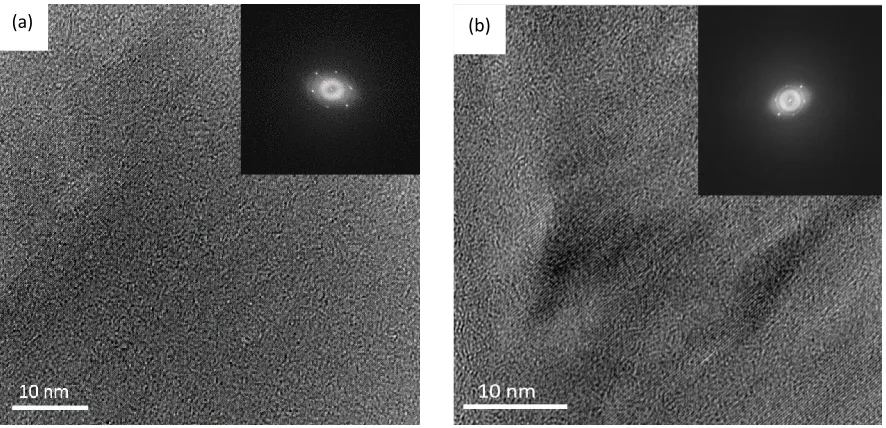
-Figure 4-6 (a) 80kV SAED image of BP flake heated to 100⁰C, (b) 80kV SAD image of BP flake heated
to 400⁰C (C) 80kV SAD image of BP flake heated to 500⁰C totally amorphous (Red Phosphorus). 52
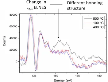
-Figure 4-7 EELS spectra showing a change in L₂, ₃ ELNES at 500⁰C indicating a difference in bonding
structure (Red Phosphorus). ... 52
-Figure 5-1 Crystal structures of α-PbO (P4/nmm, a = 3.9748 Å, c = 5.0227 Å, ICSD- 94333) and β-PbO
(Pbcm, a = 5.8931(1) Å, b = 5.4904(4) Å, c = 4.7528(1) Å, ICSD-60135). Pb atoms are shown as blue
spheres and O atoms in red. The distances of adjacent Pb layers are drawn with lines for
-Figure 7-1 (a) (b) SEM images showing the application of SEMGlu around the surrounding windows
of the MEMS chip using a Kleindiek micromanipulator needle. ... 68
-Figure 7-2 (a) e-beam Pt deposition, I-beam Pt deposition, (b) large trenches and side trench (c)
undercut ... 68
-Figure 7-3 (a)(b) showing SEM & FIB images respectively of the correct positioning of the
microgripper prior to liftout ... 69
-Figure 7-4(a) SEM images taken at 3 kV showing the micro-gripper approaching the lamella (b)
gripping lamella (c) lifting out lamella from the bulk sample ... 70
-Figure 7-5 (a) (b) SEM images showing the final stages of the thinning & polishing process of the
lamella (c) & (d) displaying the classic staggered approach to the thinning process, allowing the
thicker segment to create a gap between the thin part of the lamella and the surface of the chip, (e)
the lamella thinned at 15 kV 200pA and (f) at its final stages of polishing with a 5 kV 20pA beam. In
figure 7.5 (c) (d) (e) (f) the highlighted rectangular frame indicates the live selected milling area of
the lamella in each figure. ... 71
-Figure 7-6 (a)(b) showing the transfer of the lamella from the grippers to the MEMS chip, (c)(d)
images showing the high kV curing of the lamella and SEMGlu ... 72
-Figure 7-7 (a) shows an overview TEM image of the PbO lamella (b) HRTEM image of PbO lamella
placed over the throughhole window ... 75
Figure 78 TEM images of PbO Lamella during heating experiment. ... 76
-Figure 7-9 (a) STEM image PLD PbO lamella thin film, (b) integrated EDX spectrum profile of all 6
areas analyzed (c) line profile of inter face between analysed area 1 (PbO ) and area 2 (substrate) .. -
78
-Table of -Tables
Table 1.The decomposition temperature of PbCO3 to orthorhombic β-PbO as a function of acceleration voltage and electron beam dose ... 59
Table 2. XRD data and particle sizes of solgel synthesized PbO [84] ... 60
Table 3. Complete set of parameters for lamella preparation ... 73
-Table 5 shows results of experiments that compared various substrate materials used for the growth of
-Introduction
In-situ heating experiments in Transmission Electron Microscope (TEM) and Scanning Electron Microscope (SEM) enable real-time observations of thermally activated processes such as the evolution of stress in thin films [1] recrystallization processes [2], abnormal grain growth [3], inter diffusion [4] dislocation propagation [5] and in-situ material synthesis [6] .
However, until now most TEM specimens used for in-situ experiments have been 3 mm diameter samples prepared by conventional preparation techniques or by means of drop casting the sample in solution onto a TEM grid. These dispersions directly onto the TEM grid are difficult to control and tend not to be very repeatable. Such specimens geometries and lack of process control make in-situ heating experiments very challenging. As both of these preparation techniques require the entire 3mm sample to be heated during analysis, it is difficult to accurately control the heating at the test specimen. The heating of the entire sample also results in sample drift during analysis due to the thermal expansion of the sample holder.
Preliminary experiments in the furnace type heating stage in SEM resulted in a number of these issues. Although water cooling was used to mitigate excessive heating of the specimen stage, it became very difficult to balance heating power and cooling rate to set an equilibrium temperature.
Recent developments in Micro Electro Mechanical Systems (MEMS) based heating stages opens new opportunities for easy fast and reliable in-situ heating experiment [7][8]. Furthermore this MEMS technology can be enhanced by Focus Ion Beam (FIB) circuit edit to allow electrical measurement, contacting of materials using electron beam and ion beam deposition using FIB.
1.1
Two Dimensional Materials
In this thesis, two dimensional (2D) materials are broadly defined to include multilayers, hetero-structures, nano-flakes, nano-sheets and layered thin films whose total thickness vary from an atomic layer to tens of nanometers.
2D materials have applications in a wide variety of areas from electronic devices to catalysis, and from information storage to medicine. There is a large array of 2D materials now being researched following on from the isolation of graphene in 2004 [9]. With such a multitude of materials available, conducting, insulating and semiconducting materials monolayers comprising of single elements such as phosphorene, borophene, germanene and silicene are currently being investigated. Other 2D materials feature different atoms alternating in the same layer some examples include boron nitride, transitions metal dichalcogenides (TMDs) and MXenes. The combination of 2D layers into van der Waals heterostructures in which different monolayers are freely mixed and matched further expand the opportunities for exploring new physics and applications [10]. Electronics applications are at the forefront of most researchers work with 2D materials such as graphene because of the exceptional electron mobility. 2D materials have great potential as Field Effect Transistors (FET) channels because of their high carrier mobilities but also their large on/off ratios at low voltages they also enable the miniaturisation of FETs. Other 2D materials applications draw on the charge of the electron to encode information and spin-electronics, which leverages the spin in electrons. Valleytronics is also emerging as a way to exploit the valley degree of freedom which specifies the energy extrema, or valleys that an electron occupies to store and process information in 2D layers, the valley pseudospin can be addressed both optically and electronically to realise devices. However there is more to 2D materials than electronic devices. Graphene and more generally carbon based materials are being actively pursued as low cost efficient catalysis for clean energy production and storage. Their performance rivals that of their metal based counterparts which are costly and have relatively poor stability[11].
A new material phosphorene has recently gain a lot of interest, monolayers of black phosphorous which have anisotropic lattice that differentiates this material from other 2D materials were first synthesised in 2014 are attracting considerable interest because of its excellent carrier motilities and high optical and UV absorption [12]. Some of the properties predicated for phosphorene such as super conductivity still await experimental verification, however high performance devices such as FETs and photodetectors have already being demonstrated. Some other new 2D materials which have been reported even more recently such as borophene which has recently been isolated, which is bendable and stretchable and may be applicable in flexible electronics [13].
2D materials continues to be studied due to the wealth of unusual physical phenomena that occur when charge and heat transfer is confined to a plane.
conductors analogues of graphene/ graphene (the sp²/ H terminated sp³ derivatives) such as silicence [15] and germanane [16] have been reported. These materials similar to graphene show distinct differences between the material in its bulk form and in a single layer. These newly synthesized materials are useful building blocks that can be restacked and integrated into composites for a wide range of applications.
1.2
Structure and Synthesis of two-dimensional materials
The ability to synthesise single layer and few layer 2D materials is an essential first stop to enable the characterization of layer dependent changes, their physical properties, as well as providing information to enable these materials to be integrated into multiple applications. In general there are three main classes of materials that can be prepared as a single atom or single polyhedral thick layer.
1.2.1
Layered van der Waals solids
These are the most common class of crystalline structures that can be exfoliated as stable single layers. The crystal structure of these materials feature neutral single atom thick or polyhedral thick layers of atoms that are covalently or ironically connected with their neighbouring atoms within each layer, layers are held together via van der Waals bonding along the third axis. The weak van der Waals energies (~40 -70 meV) enable the facile exfoliation of these layers. The most common approaches for obtaining single and few layer thick 2D materials from these solids is by mechanical exfoliation using “scotch tape”, chemical exfoliation by dispersion in a solvent with the appropriate surface tension and molecule/ atom intercalation in order to exfoliate these layers and enable their dispersions in polar solvents. These mechanical exfoliation processes have been used to prepare and study the properties of few layer van der Waals materials, such as MoS₂ and NbSe₂, since the 1960 [17] . The isolation of individual and few layers using mechanical exfoliation remains the most powerful approach for studying the materials properties due to the fact it is less destructive than other methods and can create large single layer flakes (10μm ) on a variety of substrates.
1.2.2
Layered ionic solids
The second class of material that can be prepared as single or a few layers are solids that feature bulk crystal structures with charged 2D polyhedral layers that are typically held together with strong electro positive cations or strongly electronegative anions such as halides or OH
־
. To enable their dispersion as single layers in solution, these cations \ anions are typically exchanged with bulky organic cations \ anions, such as tetrabutylammonium\dodecyl sulfate. These materials can then be easily dispersed onto substrates, with the majority of materials depositing as single to a few layers. Typical examples of these materials are layered double hydroxides such as Al−NO3, Zn2Al−NO3, Ca2Al−Cl, LiAl2−NO3, Zn2Cr−NO3, and Ni2Al−NO3.1.2.3
Surface Growth of Non-layer material
1.2.3.1 Solution – Phase growth
Solution – phase metal such as solvothermal or colloidal growth reactions offer a facile production method to synthesis gram scale quantities of 2D materials with precise thicknesses and basal–plane sizes[18] . In monoclinic, rhombohedral, tetragonal, and trigonal/hexagonal systems there is one unique axis (sometimes called the principal axis) which has higher rotational symmetry than the other two axes. The basal plane is the plane perpendicular to the principal axis in these crystal systems. The crystal structure and symmetry play a critical role in determining many physical properties, such as cleavage, electronic band structure, and optical transparency.
A solvothermal process can be defined as a process in a closed reaction vessel inducing a decomposition or a chemical reaction(s) between precursor(s) in the presence of a solvent at a temperature higher than the boiling temperature of this solvent.
Current synthetic strategies for nano-sheets primarily focus on solution-based processes, such as solvothermal reactions. However, the solution-produced nano-sheet may have solvent residues adsorbed at the surface that are difficult to remove and can substantially modify the nano-sheet's intrinsic properties.
1.2.3.2 Vapour Deposition
Vapour Deposition stand as an appealing versatile synthetic strategy. However the development of a controlled synthetic method of producing 2D material such as 2D chalcogenides by vapour deposition requires a better understanding of the fundamentals involved. While vapour deposition has been extensively used for the growth of thin films and nanomaterials [19], nanotubes[20] and graphene[21], knowledge obtained from these materials may not simply be apply to 2D materials. Unlike typical nanomaterial whose growth is primary governed a catalyst, the vapour deposition of 2D chalcogenides is often non-catalytic[22] . Without the dominance of catalysts the growth of 2D nano-sheets is subject to strong influences of many experimental parameters that may play only a negligible role in catalytic growths. For example, the diffusion of source material vapour through the gas flow boundary layer strongly controls the vapour deposition growth of GeS nano-sheets. This boundary layer diffusion is found to be the rate-determining step of the growth under typical experimental conditions, evidenced by a substantial dependence of the nano-sheet's size on diffusion fluxes. It has also been shown that high quality GeS nano-sheets can grow only in the diffusion-limited regime, as the crystalline quality substantially deteriorates when the rate-determining step is changed away from the boundary layer diffusion[23]. The growth of single layer substrate wide 2D materials is essential for commercialisation [24].
1.3
Characterisation of two dimensional materials
appropriate band alignment to quench nearby fluorophores via FRET mechanism or charge mechanism. One can locate a single layer of 2D materials on a substrate by monitoring the reduction in fluorescence intensity of a thin fluorophore layer that was spun coat on top[26]. Atomic Force Microscopy (AFM) is a powerful technique to determine layer thickness with a precision of 5%[27]. However discrepancies can arise from differences in the interaction of the tip with the sample substrate[28]. Raman Spectroscopy is a method for finger printing a material and detecting layer dependent changes of the vibrational structure. It is necessary to use low power when obtaining Raman spectra of single layers to prevent sample decomposition[29].
Transmission Electron Microscopy (TEM) can provide detailed information on the nature of crystallinity layer sizes, interlayer and elemental composition. Many techniques such as Selected Area Diffraction (SAD) can be used to distinguish between monolayer and multi-layer materials. The deviation in diffraction intensity can distinguish between single and multilayers when there is a change in interlayer registration[14]. Recently advances have shown that weak field dark field electron microscopy can quantitatively determine the layer number and stacking order of multilayer graphene [30]. Scanning Transmission Electron Microscopy (STEM), using high angle annular dark field detector coupled with Electron Energy Loss Spectroscopy (EELS) can be used to visualise individual atoms in an isolated layer [31]. The ability to used low accelerating voltages (< 60KeV) minimises damage [32]. A detail description of TEM is given in chapter 2.
Scanning Tunneling Microscopy (STM) is a probe based technique that can measure the electronic and topographic structure of single atom–thick materials and can manipulate single atoms at specific points in order to build and characterise nanostructures that are well resolved from the substrate. X- Ray Diffraction (XRD) both small angle X-Ray scattering (SAXS) and wide angle XRD can supply information about the unit cell structure and constituents, the sheet thickness and lateral dimensions, and the arrangement of restacked nano-sheets[33][34][35].
1.4
Characterisation Opportunities
The development and implementation of new characterisation techniques that can rapidly and non-destructively probe atomic structures, defects and properties of single layer material is necessary to advance the field. Since the electronic properties of materials are often dominated by minority defects, the discovery, availability and implementation of techniques that can identify minority species, defects and edge states, such as aberration–corrected STEM as well as STM, will prove incredibility valuable.
New opportunities now exist due to a shift from post mortem characterization to live or in-situ measurements of structures, chemistry and properties of nanomaterials. This shift is mainly due to the adoption of aberration correction and Micro-Electro-Mechanical Systems (MEMS) device integration.
also reflected in the exponential growth in the number of publications in recent years as shown in figure 1-2 and the fact that each major materials related conference has at least one session related to in-situ TEM[36].
Figure 0-1(a) External stimuli currently used for in-situ observations on a TEM platform[37] (b) breakdown of the various
sub categories of in-situ papers presented at the Microscopy and Micro analysis conference USA 2012 and the European
Microscopy and Microanalysis conference (UK)[37]. These subcategories are in-situ electrical biasing, electron beam
heating, Thermal heating, gaseous environmental, liquid environment, mechanical loading and laser stimulation. (a)
[image:16.595.113.431.126.482.2]Figure 0-2 The growth in numbers of publications during 1988 and 2016 identified using keyword ‘’in-situ TEM’’[38]
For successful in-situ measurements the key requirement is the base unit TEM / STEM as discussed in chapter 2 which combines high spatial and spectral resolution and has the capability to be interfaced with peripheral equipment. This equipment is available from a number of vendors such as Dens Solution , Proto-chips, and Humming bird which all enable in-situ experiments similar to those outlined in the sub categories in figure 1-1(a). In addition, there is a need for a data acquisition and processing system that can improve temporal resolution and is capable of handling large data set obtained during experiments.
1.5
In-situ heating in TEM
1.6
Specimen heating holders for successful in-situ TEM
The most important features required for in-situ TEM heating is the ability to reach high temperature, and good mechanical and thermal stability of the system at high temperatures. Any instability of the holder causes a drift of the specimen. In addition if the maximum heating temperature achievable by the heater is low, the application range will be limited. Therefore the design of the specimen heating holder is the most critical issue for performing in-situ heating for TEM experiments [39]. Chapter 3 describes in detail the Dens Solutions TEM heating holder that utilises MEMS technology use for experiments in this thesis.
2
Instrumentation and Theory
2.1
Electron Microscopy
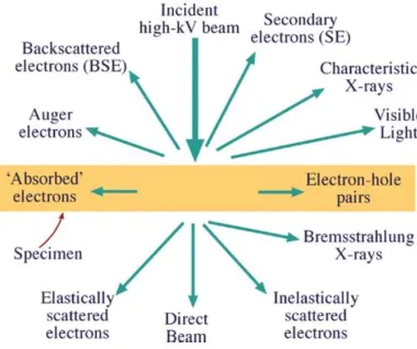
[image:18.595.191.381.524.683.2]The fundamental operation of electron microscopy relates directly back to the physics of the electron interactions with the sample. Energetic electrons are described as “ionizing radiation”. This means the radiation that is able to ionize or remove the tightly bound inner shell electrons from a material. The advantage of this type of microscopy is the range of interactions which occur and the different signals which these generate: secondary, backscattered, Auger, X-ray as shown in figure 2.1. The early stages of research in electron microscopy in the 30’s and 40’s led to the development of two distinct groups of electron microscopy: transmission electron microscopy (TEM), which also includes scanning transmission electron microscopy (STEM) and scanning electron microscopy (SEM) [40].
2.2
Transmission Electron Microscopy
Electron microscopy was developed in order to create better resolving power than visible-light microscopes (VLMs). Initially TEMs were used as their resolution is much better than visible-light microscopes (VLM). It was later discovered that the TEM can be beneficial in other ways than just better resolution. From the interactions with the incoming electrons, chemical and structural information can be obtained by utilizing the different interactions happening within the sample when the high intensity electron beam passes through it as shown in figure 2-2 [41] [42].
TEM is a technique used to acquire high spatial resolution images as well as structural and spectroscopic information from electron transparent samples[41].The microscope directs a parallel beam of high energy, typically 80 – 300KeV, electrons at the sample. In order for the simplifications associated with single scattering of electrons within the sample to be valid the sample must be typically less than 100nm in thickness, but this can vary depending on the analysis required, the mass of the atoms in the material and the energy of the illuminating electron beam.
Figure 2-2 (a) Different scattering mechanisms from a bulk specimen, typically used in SEM, (b) Different scattering
mechanisms for a thin, electron transparent, sample typically used in TEM. [41]
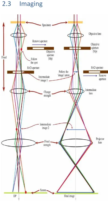
2.3
Imaging
The TEM instrument contains 3 main sections: the illumination system, the objective lens/stage and the imaging system. The illumination system consists of the gun and the condenser lenses. This system can be operated in two different modes: parallel beam or convergent beam. Parallel beam refers to traditional TEM mode and convergent refers to Scanning Transmission Electron Microscopy (STEM). In parallel mode, the most commonly used mode of TEM, uses its array of electromagnetic lenses to create a parallel beam of electrons, which pass through the sample (transmit). This electron beam collides with the electron transparent sample (<100 nm) and numerous interactions occur. There are both elastic, inelastic collisions, coherent, incoherent, elastic and inelastic scattering. The different types of scattering can help produce images and data containing different but often complimentary information. We can distinguish between imaging mode or diffraction mode as shown in the schematic Figure 2-3 [41] [42].
2.4
Amplitude Contrast
[image:20.595.68.248.73.410.2]As the electron wave passes through the sample its amplitude changes, this gives rise to image contrast, which is the difference in intensity between two adjacent areas. There are two types of amplitude contrast: mass-thickness contrast and diffraction contrast. The apertures in the TEM can be used to select certain transmitted beams and omit others in order to form different types of contrast. After the incident beam interacts with the sample it is transformed into a non-uniform intensity. This change in intensity translates into contrast in the image. The diffraction pattern shows this variation in intensity as it separates the direct beam from the diffract beams, which have been scattered throughout the sample. The diffraction pattern is only showing the electrons which have undergone Bragg diffraction. By using the objective aperture different beams (direct or diffracted) can be selected to create contrast within the image and highlight certain regions of the sample. This is what leads to bright and dark field imaging. In bright field (BF) imaging the high order diffracted beams are removed, meaning the more diffracted thicker material or defects appear darker. Conversely, in dark field (DF) imaging the beam is tilted so that the diffracted beam is allowed pass through the aperture. This makes the image
Mass-thickness contrast is due to a difference in the thickness in regions of the sample. It arises from the incoherent elastic scattering (Rutherford scattering) of electrons. As Rutherford scattering is a strong function of the atomic number Z, it is strongly dependent on the mass of the sample and also the thickness of the specimen. In a BF image, thicker regions will appear darker and thinner brighter and vice versa for DF images. [42]
Figure 2-4 Set-up of bright and dark field imaging [41]
2.5
Phase Contrast
2.6
Scanning Transmission Electron Microscopy
By combining the TEM and the SEM technology, a STEM is created. STEM mode uses a convergent probe to scan across the sample point by point. The main advantage of using STEM is the Z-contrast mechanism. STEM uses annular detectors beneath the sample which can detect electrons scattered at high angles. There are 3 different types of detectors used in STEM: bright field (BF), annular dark field (ADF) and high angle annular dark field (HAADF). Z-contrast is obtained by detecting the electrons scattered at high angles, therefore the HAADF detector is used to collect these electrons and created a dark field z-contrast image. The ADF collects electrons that are both Bragg and Rutherford scattered creating a mixture of diffraction and z-contrast. The bright field detector detects the directly transmitted beam and the very low-angle (inelastic incoherently) scattered electrons. These inelastic incoherently scattered electrons are what is used in Electron Energy Loss Spectroscopy (EELS) analysis [41][42][43].
Figure 2-5 Diagram of the imaging system and detectors in STEM [42]
2.7
Electron Energy Loss Spectroscopy (EELS)
EELS requires a high energy beam of electrons with a narrow range the electrons of known kinetic energies. An electron spectrometer is then used to measure the energy loss of the electrons which undergo inelastic scattering in the sample. An electron spectrometer uses electric or magnetic fields to bend the path of incoming electrons. Electrons with higher kinetic energy pass through the spectrometer faster and are therefore deflected less. This allows us to spatially resolve electrons with different energies.
therefore be used to quantitatively identify sample composition, and unlike Energy Dispersive X ray analysis (EDX) it is best suited to elements with a low atomic number such as carbon. In fact EELS can even be used to distinguish the different allotropes of carbon [45][43].
2.8
Review of the applications of TEM and the influence of charged particle radiation on
modifying nanostructures
TEM has been developed to a level that it can investigate the structure of material down to an atomic scale. Conventional techniques such as bright field, dark field imaging, diffraction and high resolution imaging coupled with analytical techniques such as Electron Dispersive X-ray (EDX), Electron Energy Loss Spectroscopy (EELS) and electron filtering imaging further extend the application of microscopy techniques from
microstructure, crystallography, composition, to techniques that provide information about the materials electronic structure and even optical and magnetic properties from regions of the sample in the micrometer to sub nanometer range[46]. The radiation effect of the electron beam must be considered at all times when validating these results, however the radiation effect can also be applied to tailor the microstructures and hence modify the material under examination[44]. The radiation effect in charged particle microscopes is generally considered to have a damaging and negative impact on the material under observation as it is capable of introducing undesirable disorder and thus deteriorate the material, however if we control and limit the electron beam dose, beam energy we can use this effect to modify the nano-structure of materials and observe self-organization, self-assembly of materials thus locally engineering the phase transformation of materials by the simultaneous application of thermal stimuli and localized electron beam as outlined in chapter 5.
The radiation effect has also been reported to be used to tailor the mechanical [47], electronic [48] and even magnetic properties [49] of materials at atomic precision which cannot be achieved with conventional macroscopic tools.
Electron beams on field emission guns can be focused on a spot as small as 1Å which is less than the distances between atoms in materials. However it should be also noted that modifications can also be achieved by the defocusing of the beam. The limited size of the nanomaterial in one or two dimensions needs to be
considered, as defect generation by charge particle irradiation differs in nano-materials compared to bulk materials due to the interactions of the electrons that can pass through low dimensional materials without inelastic scattering which in turn leads to very little energy loss opposed to bulk systems where all the energy is eventually absorbed. This means that the probability for energy loss of the incident beam is small in low dimensional materials and decreases with increasing energy resulting in low damage to the material when the particle energy is high, provided that displacement cascades do not play a considerable role [50]. This reduced dimensionality may give rise to a different temperature profile after the impact so that the local temperature may exceed the melting temperature of the material [51].
Electronic excitation or ionization of individual atoms Collective electronic excitation such as Plasmon Breakage of bonds or cross linking
Generation of phonons, leading to heating of the target Displacement of atoms in the bulk of the target Sputtering of atoms from the target
These radiation effects can be divided into those that lead to a displacement of atoms known as “knock-on effects” and alternatively radiation effects caused by “excitation”. Generally as the electron beam energy decreases the excitations increase whereas knock-on effects decreases. This gives us a strategy to minimize the knock-on damage during TEM experiments by lowering the acceleration voltage. Moreover this increases the possibilities of excitations which is the major origins of EELS spectrum, it also improves signal to noises ratios for chemical analysis. When the elastic scattering cross section increases, we note an increase in contrast of light elements in high resolution, zero-loss images. However when low-energy electron microscopy is applied to achieve the atomic resolution there is a need to use either direct or indirect aberration correction to achieve the required spatial resolution. Krivanek et al. [32] applied aberration correction STEM to reach probe sizes close to 1Å at 60KeV an operating energy that avoids direct knock on damage in materials consisting of light atoms. The results presented by Bell et al. [52] indicate that decreasing the acceleration voltage from 200KV to 80KV in a mono-chromated aberration-correction microscope enhanced the contrast while retaining sub-angstrom resolution.
Figure 2-6Classification of radiation damage according to the type of electron scattering and according to the effects produced in a specimen [53]
Electron scattering represents electrostatic deflection of incoming electrons by the coulomb field of each atom nucleus. This is what gives rise to electron diffraction patterns and to diffraction and phase contrast in TEM. In some circumstances elastic scattering results in atomic displacement within a crystalline specimen or electron-beam sputtering from its surface.
3
In-situ Heating Holder
In this chapter we give an overview of the major components and performance specification of the in-situ heating holder under various conditions. We present our experimental data on the observed flexural distortion of the MEMS chip during heating, and detail a novel method to enable electrical testing of materials in SEM using a circuit edited modified standard heating MEMS chip.
The in-situ heating holder is a modified TEM sample holder that interfaces and connects between EM heater chips and a control unit to enable temperature control of the EM heater chip micro hot plate from the outside world, this holder ‘’Wildfire in-situ heating holder ’’ is commercial available from Den Solutions. The materials used in the manufacture of the holder have been specially selected for optimal mechanical strength, low thermal expansion and durability. The TEM holder is specifically designed to provide in-situ heating capabilities up to 1350 °C. It utilizes small MEMS semiconductor device (consumable) as a heater. The system is optimized to have a direct read-out of the temperature value during the experiment (independent of the heater environment) with a known reproducible distribution over the heated area for heating experiments on nanoparticles and FIB lamella.
The system can heat the specimen in S/TEM and control the temperature environment of the specimen in an accurate, fast, and reliable manner such that the full characterization power of S/TEM can be used for directly observing the structure evolutions at various temperatures.
Heating plays a significant role on the structure, properties and performance of materials. However the dynamic states of materials during heat treatments cannot always be inferred from S/TEM examination at room temperatures or from postmortem studies. Therefore direct observation of the structure evolution during the heat treatment are of the utmost importance.
The heating systems contains three major components as outlined in figure 3.1a.
(1) EM heater chips (2) In-situ heating holder (3) Control unit
3.1
EM-heater chips
Figure 3-1(a) Diagram of the heating holder (b) SEM image of MEMs chip taken at 20KV using the secondary electron
detector.
3.2
Control Unit
The plug and play control unit consist of a compact electronic regulator and graphics user interface software installed on a laptop. The regulator inputs power to heat the EM heater chip and supervises the real time temperature change. A feedback loop is constructed in the regulator to quickly within 2 seconds stabilize the fluctuations of temperature less than 10mK.The graphics software allows users to input setting temperatures digitally. The software also allows the user to program temperature versus time profile to enable auto-heating experiments. The digi-heater software provides a graphical user interface for accessing the heater control box. The control box regulates with the EM-heater via the contact between the four electrical contact pads of the heater and a resistive thermometer. Figure 3-2(a) shows a plot of the temperature of four point resistance measurement versus temperature.
(a)
Figure 3-2 (a) Plot of four point resistance measurement versus temperature.
The observed advantages of Dens solutions MEMS are as follows:-
State of the art 4 point probing with continuous feedback for reliable temperature. Extremely fast response, reliable and reversible behavior resulting in no contamination or
interference.
5 X 20μm electron transparent windows for experimental freedom.
Windows are available with silicon nitride membranes less than 20nm, Carbon membranes less than 5 nm and through hole.
3.3
Temperature setting and Temperature control
Once a request to set a certain temperature is sent by the software, the control box will apply a current through two of the four contacts of the spiral heater, inducing Joules heating. The voltage between the other contacts is measured in real-time and the resistance is calculated to provide the measured temperature T of the heating element according to the Callendar-Van Dusen see equation 1 below [55][56][57][58].
(T) = AT²+BT+
C (1)This equation shows a direct and well-defined relationship between resistance and temperature for a metal-based heating element above 0⁰C. Based on the feedback of the measured temperature (calculated from the measured resistance), the control box adjusts its input current accordingly, to make the measured temperature match the set one. The feedback loop is running to compensate for possible temperature disturbance, such as change of gas pressure or a change to the sample.
A,B,C parameters in Callendar-Van Dusen equation of the EM-heater chip are parameters characterised by inherent property of the heater material. They are obtained from temperature-resistance calibration. A typical calibration can be firstly setting a temperature of the heater, e.g. by putting the heater chip in a furnace , then measuring the corresponding resistance of the heater, after a series of measurements A,B,C parameters are obtained based on the regression of the measured temperature resistance plot as shown in figure 3-2(a). The other way of calibration can be that applying current to enable the Joules heating of the heating chip, reading the resistance of the heater by four-point resistance measurements, and measuring the corresponding temperature using noncontact thermometry method, e.g. Raman or infrared thermometry to cross-correlate and built up the temperature–resistance relationship. The relationship between resistance (R) and temperature (T) is generated from the Callendar-van Dusen equations [56][59].
For the temperature range between -200°C to 0°C is describe by equation 2, for the temperature range 0°C to 661°C is described by equation 3.
𝑅𝑇 = 𝑅0{1 + 𝐴𝑇 + 𝐵𝑇2− (𝑡 − 100)𝐶𝑇3} (2)
𝑅𝑇= 𝑅0{1 + 𝐴𝑇 + 𝐵𝑇2} (3)
Where 𝑅𝑇 = Resistance at Temperature (T),
𝑅0 = Resistance at 0°C,
T =Temperature in °C
A = α x { 1+ (δ/100)} °C-1 B = - α x δ x 10-4 °C-2 C = - α x β x 10-8 °C-4
(β is equal to 0 when T is greater than zero)
Where (α) is the temperature coefficient of resistance obtained by measuring the heater resistance at both 0°C & 100°C as shown in equation 4, (δ) is obtained by calibration at a high temperature, for example, the freezing point of indium, tin, zinc, or aluminium (156.5985°C, 231.928°C, 419.527°C, and 660.323°C respectively), (β) is obtained by calibration at a negative temperature, for example, triple point of mercury and argon (-38.8344°C and -189.3442°C respectively) or liquid nitrogen (approximately -196°C).Choosing the high and low temperature point which best suites your application range improves the R vs. T correlation when applying the formulas. Using α, δ, and β, the Callendar-van Dusen equation can alternately be written as shown in equation 5:
𝑅𝑇 = 𝑅0{1 + α[𝑇− δ ( 𝑇 100) (
𝑇
100− 1) − β ( 𝑇 100)
3
( 𝑇
100− 1)]} (5)
3.4
Metal or Ceramic heater
The heater material has crucial influence on heating system performance. Two types of heaters are commonly used metal and ceramic. Both have their own advantages and disadvantages.
Metal heaters have been widely used in our daily life e.g. kitchen, industry furnaces, in the temperature range RT-2000 ⁰C. Metal is a very good conductor with quick heating response. The fast response is important for achieving effective feedback control loop. In the feedback control, the temperature of the heater is measured and corrected in real time by supervising the resistance of the heater.
It requires both the voltage and the corresponding stable current to be measured accurately and simultaneously. The shorter response time is, the faster the feedback loop can be. Long response time slows down the feedback loop, in the worst cases it may cause the failure of the feedback mechanics as its speed cannot follow the environments change. Metal heater has almost uniform performance throughout the whole temperature. However, it becomes unstable physically and chemically when the heating approaches the metal’s melting point. Ceramic is usually used as high temperature materials above 1000⁰C, as it has different properties from metal. Ceramic is chemically stable at high temperatures. With increasing temperature, the electrical conductivity of the ceramics becomes better. However, at low or moderate temperatures around 500⁰C, the conductivity of ceramics is poor and more importantly the response time of ceramics is slow, making it is difficult to achieve effective feedback control. The heater system from (DENS solution) uses metals with high melting points as heater materials to harvest the benefits of using metals and at the same time overcome it challenges. EDX analysis of the MEMS heater material found the material to be Molybdenum, figure 3-3 shows the MEMS structural properties and physical properties.
𝛼 =(𝑅100 − 𝑅0 ) (100 𝑥 𝑅0 )
Figure 3-3 shows the MEMS structural properties and physical properties
3.5
Difference between Resistance or Power dissipation as temperature indicator
Using ΔR/R relative change of resistance and not absolute resistance as temperature indicator offers a big advantage over using power dissipation because the resistance is independent of the external environment and the type or the amount of sample loaded. For instance, setting a heater at 500 ⁰C in 10‾⁷ mbar vacuum, the power dissipation of the heater is typically 6 mWatts, the measured resistance of the heater is typically 350 Ω; whereas setting a heater at 500 ⁰C in 10‾² mbar air gas environment, the measured power dissipation of the heater can be as high as 19mWatts, but the measured resistance of the heater remains the same. Figure 3-4(a) shows a plot of relative resistance change versus the dissipated power in vacuum and air for a Dens heating MEMs chip.
0 5 10 15 20 25 -0.05 0.00 0.05 0.10 0.15 0.20 0.25 0.30
Relative
cha
ng
e (
R/R)
Dissipated Power (mW)
Vacuum
Air
Figure 3-4 (a) Plot of relative resistance change versus dissipated power in Vacuum and Air for DENS heating MEMS Chip.
In contrast, the resistance temperature relationship, well defined by Callendar-Van Dusen as shown equation 1 (page 27) is independent to the external factors other than temperature.
This is why the DENS solution MEMS uses resistance as a temperature indicator, allowing the calibration parameter obtained in the calibration environment to be applied to the heater chip in various working environments.
3.6
2 Contacts or 4 contacts measurement
For measuring the resistance, 2 contact or 4 contact resistance measurement can be chosen. In the two contact resistance measurement figure 3-5(a), the total resistance of the system is actually measured, including the resistance of the micro-heater, the resistance of the cables that connect the heater to the outside regulator, the resistance of contacts from mechanical connections of various cables and needles to the chip interface resistances. As the cables and the contacts may be in a temperature environment different from the micro-heater (note that some part of cables are even outside microscope) and the material of the cable and the micro-heater may be different, the total resistance method cannot be directly used to link the temperature of the micro-heater. For these reason the DENS solutions heating holder uses four contact resistance measurement method as show in figure 3-5(b) for obtaining the resistance of the heater. This method excludes the influence of the cable resistance and the uncertain contact resistance, allowing the measurement resistance to be used to indicate the temperature of the microheater.
Figure 3-5 (a).Two point contact resistance schematic which does not take account of total resistance of complete electrical setup during analysis (b) Four point contact resistance schematic for heating holder which takes account of the total resistance of complete electrical setup during analysis.
3.7
Temperature gradient across the MEMS device
Heating is localized around the centre of the micro-hotplate. The temperature 300µm away from the edge of the micro-plate drops to room temperature as shown in figure 3-6. The micro scale heating results in a power consumption of only several mWatts for reaching high elevated temperature above 1000°C. This low power consumption and localized heating dramatically reduces the sample drift during heating experiments and avoids the using water to cool down the holder. Figure 3-7(a) shows the temperature localized around the micro hotplate of the MEMS chip, figure 3-7(b) shows the mems chip in air under an optical microscope at 950°C showing the localized heating.
Figure 3-6 shows the temperature gradient profile across the MEMS device [60]
Figure 3-7 (a) showing temperature localized around micro- hotplate ,cross calibrated with resistive thermal sensor, infrared pyrometry, and Raman thermometry (b) image of mems chip at 950⁰C under optical microscope.
It is mainly the EM heater chip that determines the temperature working range and thermal drift rates, figure 3-8(a) shows data provide by DENS solutions of the amount of thermal drift over a 25 hour period. Thus, it provides the possibility to upgrade the heating system performance, by simply introducing a new MEMS. Standard MEMS chips can work up to and above 1000°C. The ultra-high temperature heating chips can work up to above 1400°C.
Figure 3-8 (a) Plot of temperature drift over a period of 25 hours, the temperature was set at 1337.0 °C on ultra-high temperature chip.
(°
C
)
Advantages of MEMS based heating holder.• The thermal stress is localised around a small inner coil. • Local heating removes excessive
thermally induced drift.
• 4-point geometry allows for very accurate and controlled
temperature measurement. • Rapid temperature elevation and
relaxation.
• MEMS chip customisation (a)
(b)
3.8
MEMS flexural distortion during heating in-situ in TEM
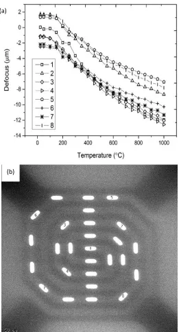
It was noted during experiments that there was a requirement to repeatedly de-focus the image each time we increased temperature. This was found to be due to the MEMs chip flexing during heating. To characterize the flexing of the MEMS chip due to heating 8 locations on the MEMS chip were selected to measure the defocus value versus the temperature at evenly distributed locations from the centre of spiral heater of the MEMS chip to the outer spiral of the MEMS chip. Figure 3-9(a) shows a plot of the resulting defocus values versus temperature at the 8 locations indicated in figure 3-9(b).
Figure 3-9 (a) Plot of defocus value at various locations on MEMS chip versus temperature (b) TEM overview of the MEM chip and the map of measurement locations.
(a)
[image:35.595.75.336.222.705.2]The measured defocus values for all 8 locations were plotted against temperature to produce a visual map of the MEMS chip flexural distortion under thermal stress. The plots shown in figure 3-10 gives an indication of the flexural distortion at a range of temperatures.
Figure 3-10 Plots of flexural distortion due to thermal stress across the area of the heater spiral of the MEMS chip.
The process was repeated for 26 locations on an through hole MEMS chip. Figure 3-11 gives an indication of the observed distortion at a range of temperatures on the through hole MEMS chip.
MEMS flexural distortion at 300°C
Figure 3-11 Plot of flexural distortion due to thermal stress across the area of the heater spiral of the through hole MEMS chip.
MEMS flexural distortion at 1100°C
3.9
In-situ SEM heating MEMS
MEMS setup in SEM to observe MEMS flexural distortion during heating
An experimental setup was developed to enable in-situ heating in SEM and also to investigate further the actual flexural distortion of the MEMS during heating. The DENS solution MEMS heating chip was attached to a SEM stub using a carbon tab. Two Kliendiek nano manipulators (MM3A) with probe tip ~100nm were mounted inside the SEM chamber and controlled through a SEM chamber feedthrough flange and standard feed through electrical connections to each manipulator and corresponding controller units. A Keithley dual source meter (2600 series) was connected in series to the controller units and use to ramp the current (I) and voltage (V) to the contact pads on the MEMS via the manipulator probe tips. The figure 3-12(a) shows the probe tips in contact with the MEMS contact pads. The voltage and current was ramped in a controlled manner however this experimental setup uses 2 point probing directly onto the MEMS chip which is not as controlled or as accurate as four point probing method used in the DENS solutions heating holder setup in TEM.
a b
c d
Figure 3-12 (a) shows the manipulator probe tips in contact with contact pads of MEMS chip (b-h) shows SEM images of the flexural distortion as heating increases in the range of 20°C to around 750°C.
Significant flexural distortion was observed as a function of temperature as the temperature was ramped from 20°C to failure temperature ~750°C figure 3-12(b-h). The flexural distortion observed in SEM followed the measured flexural distortion in TEM as shown in figures 3-10, 3-11.The higher the chip power
consumption and power density are, the more pronounced effects and surface effects are .The mismatch of heat stress is more severe ,which can cause the MEMS devices to distortion. It should also be noted in the SEM experimental setup the MEMs chip failed at a temperature lower than its specification, this was most likely due to the experimental setup in SEM and the degree of control while ramping the voltage and current.
3.10
Electrical probing on circuit edited MEMS chip in SEM &TEM
A method was developed to electrically contact samples placed on the heating MEMs chip by modifying the MEMS heating spiral. FIB was used for this purpose. The procedure was demonstrated on a Black
Phosphorous (BP) flake that was mechanical exfoliated and placed over a window on the heating MEMS chip as shown in figure 3-13. Black phosphorus is the thermodynamically stable form of phosphorous at room temperature and pressure.
Figure 3-13 Black phosphorus flake mechanical exfoliated onto MEMS chip.
Once the position of sample on the MEMS chip was determined the MEMS electrical heating spiral was modified by a series of FIB cuts to isolated two sections of the spiral circuit as shown in figure 3-14. These isolated sections of the spiral maintained direct connection to the their respective contact pads on MEMS chip thus enable electrical connectivity to the DENS Solution heating holder when performing electrical measurements in TEM and to also allowing the micro manipulator probes to make electrical measurements when set up in SEM see figure 3-12(a).
A 3μm x 3um window in the silicon nitride top layer of the MEMS chip was milled away using FIB to create an electrical contact to the molybdenum metal spiral below in the two isolated spiral section adjacent to the window where the sample was placed (see figure 3-15).
Figure 3-15 Windows exposed in silicon nitride layer to allow electrical contact
The gas injection system and FIB/SEM was used to make electrical connection between the sample and the exposed metal of the spiral in the window using e-beam platinum deposition figure 3-16(a). A resistance measurement between -10V and +10V was obtained for the BP sample flake tested in SEM using the micro manipulators and an Keithley source meter the corresponding IV curve was obtained and is shown below in figure 3-16(b).
A second BP sample was prepared using the same procedure, however this MEMS chip was placed in the Dens Solutions heating holder and the electrical measurement were made in-situ in TEM using the heating holder and electrical feedthrough connector box connected in series to the Keithley dual source meter. Figure 3-17(a) shows TEM overview of a platinum e-beam deposited contacts to BP flake. The corresponding IV curve was obtained for the BP flake under test in the voltage range -15V to +15V and is shown below figure 3-17(b).
Figure 3-17 TEM image showing sample and platinum e-beam deposition to make electrical connection (b) IV curve
After electrical testing was completed the MEMS chip was heated up to 190°C on a hotplate to see the robustness of the platinum deposition making the electrical contact between the sample and the MEMS spiral. TEM images were taken before and after heating. It was noted that the heating causes ‘’opens’’ and the potential for ‘’shorts’’ in the connections. The TEM images below figure 3-18(a) show the electrical connections before heating figure 3-18(b) after heating to 190°C on a hotplate.
a b
Figure 3-18 (a) TEM image of e-beam electrical connections prior to heating (b) TEM image of e-beam electrical connections after heating showing ‘’opens’’ .
4
An in-situ heating TEM Study into the thermal decomposition of Black
Phosphorous nano-sheets
4.1
Introduction
Ever since its discovery [61][25], graphene has been one of the most researched materials for its electronic and energy applications [62][63]. It has a very high carrier mobility (of the order of nearly 2.5 × 105 cm2 V-1 s-1), but due to its semi-metallic nature, it is impossible to completely turn the current off which hinders its application in microelectronic devices, such as field-effect transistors (FET) and computer chips. The successful isolation of graphene has motivated research in other inorganic layered 2D materials like h-BN [64] , transition metal oxides[65], graphitic oxides[66], transition metal dichalcogenides (TMDs) [17], black phosphorus (BP) [67] and post-transition metal oxides [68]. Some of these materials show properties that are rivalling or exceeding that of graphene. For example, monolayer MoS2 has a band gap of 1.8 eV and a carrier mobility of 200 cm2 V-1 s-1. But the direct nature of the band gap is not lost in any number of layers. More recently, over one hundred years after it was successfully synthesis in the bulk form in 1914[69], monolayer black phosphorus (BP) namely phosphorene, has been attracting a lot of attention as a 2D layered material, which in turn has attracted interest from condensed matter physicists, chemists, semiconductor device engineers and material scientists. Similar to graphite and TMDs, BP has a layered structure but with a unique puckered single layer geometry as shown in figure 4-1.
[image:47.595.77.541.464.709.2]Due to its intriguing properties such as moderate direct band gap (0.3eV - 2 eV), which depends on it thin film thickness, very high carrier mobility of 103 cm2 V-1 s-1 and anisotropic in-plane properties, BP looks a promising candidate for applications in nano-electronics and nano-photonics that differ from graphene and TMDs. Phosphorene’s main drawback is that it degrades in ambient atmosphere and in contact with water[71]. However, it has been reported that special treatments involving the formation of chemical or physical passivation layers can be used to overcome stability issues in exfoliated BP [72]. D. Hanlon et al., for example, demonstrated that exfoliating black phosphorous in liquid-phase in the organic solvent CHP (N-cyclohexyl-2-pyrrolidone) can increase the lifetime of the system from hours to months. The reason for such an increase in its lifetime was mainly attributed to the formation of a CHP solvation shell around the BP sheets.
The use of protective chemical or physical passivation layers is however inconvenient for all those applications which require the use of pristine flakes. In order to get insights on the mechanism involved in the BP degradation I carried out a systematic in-situ thermal TEM analysis.
4.2
Experimental Methods
In order to rule out any contribution from solvents in most cases we carried out our experiments on mechanically cleaved BP nano-sheets, transferred onto a MEMS chip. In-situ TEM was carried out in a FEI Titan300 operated at 300kV and 80kV. Furthermore, I investigated the e-beam contribution to the nano-sheets degradation. In order to do so, I worked in two different regimes: “beam-off”, meaning that the sample was heated while blanking the beam, and turning it on only for imaging post-heating; and “beam-on”, meaning that imaging was carried our while the sample was heated.
4.3
Experimental Discussions: in-situ thermal decomposition of Black Phosphorus
Figure 4-2 (a) Typical TEM image of a BP flake after heating to 350⁰C (heating occurring over the course of 10 mins) in an e-beam-off set-up (no imaging while heating). The inset shows the FFT of the same area; (b) Typical TEM image of a BP flake after heating to 400⁰C (heating occurring over the course of 10 mins) in an e-beam-off set-up (no imaging while heating). The inset shows the FFT of the same area. Both images show sign of very little degradation happening with heating, whilst the FFTs remark a very high degree of crystallinity being present.
In order to monitor the possible contribution of the electron beam, we carried out a second set of in-situ experiments, heating a BP sample this time while imaging (beam-on configuration). Figure 4-3a shows a typical TEM image of a BP flake that was heated to 450⁰C, while being exposed to the imaging electron beam for 2 minutes. This image (electron dose =4.8 x 10⁵C/cm² at a magnification of 380Kx; beam current= 8.94nA) and its corresponding FFT in the inset) demonstrate that the flake has completely lost all its crystallinity.
In contrast, figure 4-3b shows a flake that was heated to the same temperature as shown in 4-3a but without any exposure to the electron beam (beam-off configuration). As can indeed be seen in the FFT in the inset, the flake has remained perfectly crystalline and displays the expected diffraction spots.
Finally, figure 4-3c shows the same BP flake as in figure 4-3b after it had been continuatively heated at 425°C and exposed to the electron
![Figure 0-1(a) External stimuli currently used for in-situ observations on a TEM platform[37] (b) breakdown of the various sub categories of in-situ papers presented at the Microscopy and Micro analysis conference USA 2012 and the European Microscopy and M](https://thumb-us.123doks.com/thumbv2/123dok_us/948121.607917/16.595.113.431.126.482/currently-observations-breakdown-categories-presented-microscopy-conference-microscopy.webp)
![Figure 0-2 The growth in numbers of publications during 1988 and 2016 identified using keyword ‘’in-situ TEM’’[38]](https://thumb-us.123doks.com/thumbv2/123dok_us/948121.607917/17.595.92.538.63.284/figure-growth-numbers-publications-identified-using-keyword-situ.webp)
![Figure 2-4 Set-up of bright and dark field imaging [41]](https://thumb-us.123doks.com/thumbv2/123dok_us/948121.607917/21.595.76.518.182.414/figure-set-bright-dark-field-imaging.webp)
![Figure 4-1 (a) Atomic structure of multi-layer black phosphorus and (b) monolayer phosphorene [70]](https://thumb-us.123doks.com/thumbv2/123dok_us/948121.607917/47.595.77.541.464.709/figure-atomic-structure-multi-layer-phosphorus-monolayer-phosphorene.webp)