by
J~rgenStaunstrup
DAIMI PB-29
May 1974
Institute of Mathematics University of Aarhus
DEPARTMENT OF COMPUTER SCIENCE Ny Munkegade - 8000 Aarhus C - Denmark
Phone 06-128355
'== r- F""""' I
-f:=
[
H~
[
I tnli
1
~::cr
---r
d:l
'""""'bl
Wrr
r
1Foreword
1.
o.
Introduction1.1. Historical Notes
1. 2. General Design Criteria and Constraints 2.
o.
The RIKKE 1 system2. 1. The Register Group 2.2. Counter A
2.3. Bus Transport 2.4. Working Registers
iii
2
5
6
8
10 12 2.4. 1. Microinstruction Format and a Few Exampl es 14 2.5. The Bus Sh ifter
2.6. Bus Masks 2.7. Postshift Masks
2.8. The Ari thmetical and Logical Unit 2.9. The Local Registers
2. 10. The Accumulator Shifter 2. 11. The Variable Width Shifter 2. 12. Doubl e Sh ifter
2. 12. 1. Two exampl es using the shifters 2. 13. The Common Shifter Standard Group 2. 14. Loading Masks
2. 15. The Parity Generator 2. 16. The Bit Encoder
2. 18.
Output Ports2. 19.
The Bus Structure2.20.
The Control Unit2. 20. 1.
Microinstruction Sequencing2.20.2.
The Control Unit Arithmetical Logical Unit2. 20. 3.
Return Jump Stacks A and B2. 20. 4.
The Save Address Regi ster2. 20.
5.
The Microinstruction Address Bus2. 20. 6.
Control Store Loading2.21.
Control Panel Switches KA and KB2. 22.
Internal FI ags KC and KD2. 23.
The Conditions and Condition Selector2. 24.
Short and Long Cycl e2.25.
The Real. Time Clock2.26.
Auxiliary Facilities2. 26. 1.
Counter B2. 26. 2.
Main Memory2.27.
An Alternate View of the Working Registers2.28.
An Alternate View of the Postshift Masks3.
o.
Microinstruction Specification and Execution3. 1. Microinstruction Format .
3. 2. Microinstruction Execution
3.2. 1.
Exampl e of how to use Clock Pul se1
and Clock Pul se 2
3.3.
Comprehensive Tabl es of Microoperations for64
67
69
70
72
77
80
81
83
84 8486
90
91
92 9293
96
99
102
102
110
112
Individual Functional Units
113
Tabl es of Microoperations
114
Tabl e of Fi rst Occurrance of Abbreviations and Symbol s 1
21
List of Figures
125
List of Tables
127
Foreword
It is the purpose of this document to give an introductory (yet reasonably detai led) description of the RIKKE 1 System. The bus structure, the registers and functional units attached to it, and the control which can be exercised on these components are discussed. The document is not a reference manual. Rather, it is written entirely from the pedagogical point of view, with the system described in a modular fashion. Examples are introduced after each component is added to the basic bus structure. The examples are written in the RIKKE 1 microassembly language (see
[8J). The examp les are del iberately kept simp Ie so the reader wi II not spend time learning a complicated or clever algorithm but wi II learn the control mechanisms of the particular components involved. Thus, many of the examples are IIcon trivedll and do not perform any particular
"useful" data transformations. It is hoped that this approach enhances the reader's understanding and underscores the overall simplicity and homogeneity of the structure and its components.
The present description is a modification of a similar one, describing another sl ightly different system called MATHILDA (DAIMI PB-13), written by Bruce D. Shriver.
1. O. Introduction
RIKKE 1 is a dynamically microprogrammable processor which has been designed to be used as a tool in emulation-oriented and processor design research. For the sake of compl eteness we wi II di scuss bri efl y a short history of the unit and then some of the criteria which served as a basis for its design.
1.1. Historical Notes
In the spring of 1971 the Department of Computer Sc i ence of the Un iver-sity of Aarhus was considering the purchase of a standard minicomputer to act as a controller for a variety of peripherals and to simulate a me-dium speed batch terminal to the Computer Center's large system. A group of people were, at this time, working on the design of an integra-ted software and hardware description language called BPL [1
J.
To support this group and to make the use of such a minicomputer more flexible, it was decided to design and construct a microprogrammable minicomputer within the department itself.The design was started and compl eted during the summer of 1971. The resulting machine, RIKKE 0
[2J,
was constructed and began running in early 1972. In the meantime a number of projects were proposed which were considered not to be compatibl e with that design. Among these were various projects in numerical analysi s [3, 4J
in wh ich it was found that the word size and bus width of the RIKKE 0 (16 bit) was too short to obtain an efficient implementation of even standard arithmetic operations on numbers. It was then suggested that a microprogrammed functional unit with a wider data path and special features could be attached toRIKKE 0 as an I/O device, or "functional unit", together with a wider memory, for use with these projects. A proposal was made to the Danish Research Council to obtain a grant to design and construct such a func-ional unit. A grant was made i June 1972 in which funds were awarded for hardware and a memory (32K, 64 bit wide, 1.4 \-ls access time). The manpower for the construction of the un it was, in part, granted by the Research Council; two staff engineers and one staff technician were provided by the Department. The design was started in May 1972 and completed during the summer of 1972. The construction of the resulting machine, MATHILDA, is due to be completed summer 1974.
The motivation for building the MATHILDA instead of purchasing a com-mercially available machine can be summarized as follows. First, there were ( as far as we knew ) no commercially available dynamically microprogrammable processors at the time we started our efforts which: (a) were in the price range we could afford, (b) were designed for or supported user written microcode or (c) offered a reasonable experi-mental and growth ori ented structure. We fel t that we had the in-house capabil ity to design and construct the machine. The avai I abil ity of LSI
circuits and convenient mounting techniques and our experience with RIKKE 0' supported this view.
It was also decided that the new design for MATHILDE outdated the de-sign of RIKKE 0, and with only minor modifications and additions could be used in the construction of a 16-bit machine, RIKKE 1,which is the subject of this description. Design criteria with respect to construc-tion supported this view, these wi II be described in the next secconstruc-tion.
1. 2. General Design Criteria and Constraints
The RIKKE-O machine is intended to be a research oriented machine. Its main design criteria then, within the money and timing constraints on the project, was to provide a machine on which a large variety of
experiments related to processor and emulator design and evaluation could be performed. We attempted to use the "top-down" design approach
which quite frequently was tempered by th~ "forces from below", see Rosin [5J. Therefore, we tried to let various application-oriented and software ideas be reflected in the design.
Two general software concepts had a reasonabl e impact on design. The one being the ability to multiprogram virtual machines and the other being the concept that virtual machines would be defined through several layers, (e. g., R. Dorin [6
J).
The effect of these ideas is apparent in the design of the control unit, especially with respect to the capabilities of addressing. Many addressing features known on the virtual I evel are present here on the micro level.Another criterion was to have a clean and consistent way of dealing with timing probl ems. We decided not to force the speed; rather we would have a slower machine than obtainable with the componemtry at hand, and thus one, hopefull y, with a reduced set of timing idiosyncra-sies. It was also decided to be able to control all elements of the system from an immediate control or a residual control capabil ity, or some com-bination of both. The residual control was made homogeneous to the user by having a reasonably "standard control register group" where ever such control was provided.
Another design criterion dealt with the actual construction of the unit.
It had been decided, prior to the obtaining of the grant from the Danish Research Council, to construct additional RIKKE's by other funding.
It became apparent, during the design phase of MATHILDA, that the machine would be reasonably complex and that several features of
MATHILDA included or extended similar features on RIKKE O. Because of the complexity of the design, the limited funds and manpower available, and the fact that we wished to design, construct, and test the machine within 1 year, it was decided that the additional RIKKE's (now called RIKKE l's) should be modeled after the MATHILDA System. Thus, one design criterion was to ensure a modularity in the hardware design. This would enable an economy in print-layout and construction to be achieved. As an exampl e, the bus structure is I aid out on one print board, 8-bits
wide. Two of these boards, interconnected, comprise one RIKKE 1 bus
structure with all registers, shifters, etc. Four of these RIKKE 1
boards, interconnected, give the MATHILDA bus structure. (For a
description of the MATHILDA see Shriver [7]).
2.
o.
The RIKKE 1 SystemRIKKE 1, as has been stated earl ier, is a microprogrammed controlled bus structure. The major el ements of the system are shown in Fi gure 2. 1. and are the:
1) bus structure.
2) control unit.
3) auxiliary facilities.
4) I/O.
5)
Memory.In the following sections we will describe each of these systems inde-pendent! y and give exampl es of thei r uti I ization.
Figure 2. 1. RIKKE 1 System
Control Unit Control Instruction
Store Sequencing
Functional Unit or Register System Counters
L 2 v
.
Control Panel
-.
Bus ShifterUl
Switches
w
0
CO
~nternar Switches
Functional Un! t
or Register
Auxiliary Facilities
Bus Structure
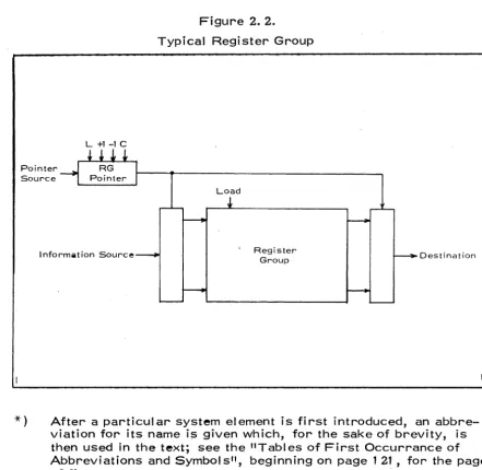
2. 1. The Regi ster Group
We begin by introducing a fundamental building block which is used in the various control mechanisms of the system, viz, a Register Group RG*, as shown in Figure 2.2. A RG is a set of 16 or 256 registers. The width of the registers and the number of registers in a specific RG will be stated when it is introduced. The element of a particular RG, which is to be used as a source or destination for the transfer of infor-mation, is pointed to by the RG address register. This register is called the Register Group Pointer, RGP, as shown in Figure 2.2.
Pointer Source
L +1 -1 C
Information Source
Figure 2. 2.
Typical Register Group
Load
Register
Group Destination
*) After a particular system element is first introduced, an abbre-viation for its name is given which, for the sake of brevity, is then used in the text; see the "Tables of First Occurrance of Abbreviations and Symbols", beginning on page
121,
for the page of first occurrance. [image:10.602.80.522.295.726.2]There are four microoperations associated with an RGP. They are marked L, +1, -1, and C in Figure 2.2. and all subsequent figures.
Tabl e 2. 1.
Microoperations for the control of an RG
Symbol ic Notation Microoperation
L RGP:=Pointer Source Load the RGP from the Pointer Source +1 RGP + 1 Increment RGP by 1
-1 RGP - 1 Decrement RGP by 1
C RGPC CI ear (i. e., set to zero) RGP
- - - _ .. --- - - -
-The symbol ic notation RGP
+
1, RGP - 1, etc. is the notation which is used with our microassembler, and all of our examples will be shown using this notation. The abbreviation 'RG' will often be replaced by the abbreviation of the name of the functional unit with which that particular RG is associated. Not all of the RGP's will have the microoperationRGP:=Pointer Source
associated with them. For those RGP's which do have this microopera-tion it will be seen that the Pointer Source data itself can usually be selected to come from any of four different sources.
There is one additional microoperation required for the control of an RG; namely the function labelled "load" in Figure 2.2. If the loading of an RG can be initiated by a microoperation it will be indicated by an "L" on such a diagram.
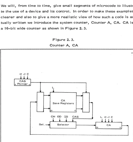
2. 2. Counter A
We will, from time to time, give small segments of microcode to illustra-te the use of a device and its control. In order to make these exampl es clearer and also to give a more real istic view of how such a code is
[image:12.609.91.530.132.601.2]ac-tually written we introduce the system counter, Counter A, CA. CA is a 16-bi t wide counter as shown in Figure 2.3.
Figure 2.3. Counter A, CA
..
+1 -1 C
L
o
CM 00 so L +1-1 C
Sel.
CA has four microoperations associated with it as shown in the box la-belled 'CAl in this Figure. These microoperations are given in Tabl e 2.2.
Table 2.2.
Microoperations for control of CA
Symbolic Notation Microoperation
Load CA from either CM, 00, S8, or CA:=CM
I
00I
SBI
CASCAS. Note the use of
"I"
to mean "or" L in the symbol ic notation for thismicro-operation.
+1 CA+ 1 Increment CA by 1
-1 CA - 1 Decrement CA by 1
C CAC Clear (i. e., set to zero) CA
- - ---_._--- - - -- - - -.. __ ... _
-Both the box labelled "Selector" in Figure 2.3. and the explanation of the microoperation "L" in Table 2.2. state that CA can be loaded from one of four possible sources:
1)
Immediate d.ta within the Current Microinstruction, CM, 2) A 16-bit Output Register, 00 (discussed in Section2.18. ),
3) Bits 0 through lS of the Shifted Bus, S8 (discussed in Section 2. S), and
4) From an element of a 16-bit wide, 16 element RG called the Counter A Save Regi sters, CAS.
Thus the microoperation
CA:=37
loads CA with the constant 37 from a data field within the CM. While the microoperation
CA:=CAS
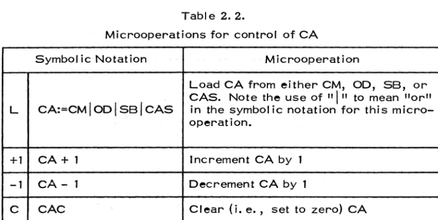
loads CA with the ccmtents of the element of CAS which is pointed to by the CAS Pointer, CASP. Notice that the CAS can be loaded with the contents of CA thus _"owing one to save the current value of CA. The four microoper~tions associated with the CAS and CASP are in Table 2.3.
[image:13.605.94.526.93.310.2]Table 2.3.
Microoperations for control of CAS and CASP
Symbol ic Notation Microoperation
L CAS:=CA Load the el ement of CAS pointed to by CASP with CA
+1 CASP + 1 Increment the CASP by 1
-1 CASP - 1 Decrement the CASP by 1
C CASPC CI ear
(i.
e., set to zero) CASP---- - - -- - - _ .. _- _ ..
-We can test to see if CA contains zero. -We wi II demonstrate the use of this condition and the microoperations in Tabl es 2.2. and 2.3. in sub-sequent exampl es.
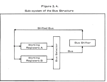
2. 3. Bus Transport
Having introduced some elementary notions we will now examine in some detail the bus structure, the registers and functional units attached to
it, and the control which can be exercised on these components. We will construct the bus structure in a modular fashion - hopefully to enhance the reader's understanding and to underscore the overall sim-pi icity and homogeneity of the structure and its components.
Let us introduce the concept of a bus transport by considering a sub-system of the bus structure consisting of the Working Registers A, WA, Working Registers B, WB, and the Bus Shifter, BS, as shown in Fi-gure 2.4. The exact nature of WA, WB and BS is not important to us here.
Figure 2.4.
Sub-system of the Bus Structure
Shifted Bus
Working
H
L2
Registers A u
ill ill (J)
Working
H
If)::J
Registers B
m
The BUS is a 16-bit wide data path. The input to the BUS (its SOURCE) is obtained from a bus selector which has eight inputs, two of which are shown here. i. e., WA and WB. The particular input which is selected as the SOURCE for bus transport may be shifted a specified amount in the BS. The output of the BS, call ed the Shifted Bus, SB, can then be stored in at least one of seven possible 16-bit destinations (called Bus Destinations, BD, or DESTINATION). Two such BD's are shown in Figure 2.4. i. e., WA and WB. We will in this report specify bus trans-port information as we do in our microassembl er, viz,
DESTINATION:=SOURCE, BS Specification.
If the BS Specification field is empty, i. e., the BS is not to be used (no shift occurs) then the bus transport is given by
DESTINATION:=SOURCE.
[image:15.595.93.530.84.417.2]As an example, the bus transport WB:=WA has the obvious meaning of a register to register transfer from WA to WB. If a SOURCE is chosen to be transported but not stored in any of the BD's, the bus transport information is written
SOURCE, BS Specification
,.
or
SOURCE
as is appropriate. The SOURCE may be stored in destinations other than BD's during a bus transport. We will learn what functional units or regi sters can serve as these "other destinations" as this report develops. If the SOURCE is to be stored in more than one destination, the DESTINATION portion of the bus transport specification is written as a I ist of destinations separated by commas,
i.
e. ,LIST:=SOURCE, BS Specification or
LIST:=SOURCE where
LIST::=d1 , • • • , dn •
The value of n and the units which can serve as destinations, d1 , will
be discussed later.
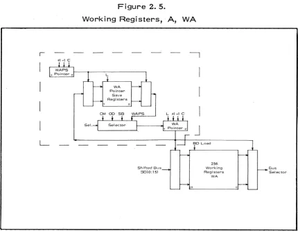
2.4. Working Registers
WA and WB, introduced in the previous section, are not single regis-ters but each is a 16-bit wide, 256 element RG. Figure 2.5. shows WA; WB, not shown, is identical.
The first thing we wish to point out in this figure is that the WA Pointer, WAP, is a mechanism identical to CA except that it is 8-bit wide and not 16-bit wide. (Note the dashed-I ine box in Figure 2.5.). Therefore, WAP not only points to which element of WA can be used as a SOURCE
for bus transport (or used as a BO), but also can be stored in an RG
I
+1-1 C
[image:17.595.94.528.134.467.2]L
Figure 2.5.
Working Registers, A, WA
Sel.
eM OD 58 WAP5 ~
Shifted Bus 58(0:15)
I
L +1-1 C
256 Working Registers
WA
Bus
Selector
called the WAP Save registers, WAPS. This is identical to CA being saved. Also, as indicated in the box labelled "Selector" in Figure 2.5. the WAP can be loaded from any of four sources:
1)
immediate data from the CM2) the least significant 8-bits from 00 *)
3) the least significant 8-bits of the SB, *) and 4) an el ement of WAPS.
This is identical to the loading of CA. Thus the microoperations WAP:= 37 and WAP:=WAPS have well defined analogous meanings.
The WA (and WB) registers are not loaded by a microoperation but rat-her as a result of being chosen as a BO in a bus transport specification; thus the loading of these registers is shown by the function "BO Load" on Figure 2. 5. Th is notation wi II be used in all subsequent drawings.
*) WB is different with respect to 2) and
:l
in the sense that loading of WBP takes place from the most significant 8-bits of 00 and SB.There are 8 microoperations shown in Figure
2.5.
ass()ciated with the use of WA. These are I isted along with the correspondingmicroopera-tions for WB in symbol ic form in Table 2.4. The actual microoperation descriptions can be extracted from the previous tables and are not repeated here.
Tabl e 2.4.
Microoperations for control of WA and WB
WAP:=CMI 000-7\ SB(Y7\ WAPS WBP:=CM
I
oDs-151 SB8-15I
WBPSWAP
+
1
WBP+
1
WAP - 1 WBP -
1
WAPC WBPC
WAPS:=WAP WBPS:=WBP
WAPSP
+
1
WBPSP+
1
WAPSP -
1
WBPSP -1
WAPSPC WBPSPC
2. 4.
1.
Microinstruction Format and a Few Exampl esIn order to present a few exampl es we will introduce the microinstruc-tion format which we use in our microassembl er. The format of a mi-croinstruction is:
"A: bus transport; microoperations and data; microinstruc-tion sequencing. ",
where
a) "A" is a symbol ic name for the address of the microinstruction,
b) "Bus transport" is a field giving the bus transport information as expl ained previousl y in Section 2.3. ,
iflifiWiii;':--c} "microoperations and data" is a field of up to 7 microoperations and immediate data to be executed or used during this microin-struction {the exact combination of microinmicroin-structions and data which can be included in this field and precise details of the ti-ming of microoperations are given in Section 3.
o.}.
d} "microinstruction sequencing" information will be written in the form
if c then
At,
el se Atwhich is to mean: if a particular selected condition c is true then choose address At as the address of the next microinstruction el se choose
At .
I t is not necessary or appropriate at this point to list all of the condi-tions which are testabl e by the system nor how At and At are funccondi-tions of the address of the current microinstruction, A. These matters wi II be dealt with in Section 2.20. 1. However, conditions and address
functions wi II be introduced as needed for exampl es. If no condition is to be considered, i. e., if At =
At ,
the sequencing information will mere-ly be written At {and not "if c then A else A II where c is anarbitra-ry condition}.
Thus, the microinstruction labelled A ,
A: WA:=WB; WBP
+
1; A+
1means: load the el ement of WA pointed to by WAP from the el ement of WB which is pointed to by WBP without shifting it during the bus transport; Then increment WBP by 1; then obtain the next microinstruction from A
+
1 . The action associated with every microoperation specified in amicroinstruction is completed before the next microinstruction is execu-ted. For example, in the above microinstruction if WBP had been set to 9 before the beginning of the execution of this instruction, then WB9 would be the SOURCE for the bus transport. At the end of execution of the instruction, the WBP woul d be set to 10. If, in the next microin-struction WB were again sel ected as the SOURCE, then the contents of WB 1 0 would be gated onto the BUS.
In order to give an example of a microinstruction using conditional branching, we establ ish the following convention for the testing of conditions which will be used in all of our examples (unless stated ex-plicitly otherwise): all conditions which arise as a result of bus trans-port and microoperation execution specified by a particular microin-struction, M, are testable in the next microinstruction to be executed after M is executed. This means that all the conditions available or changed during the execution of microinstruction M are "saved". These "saved" conditions are those tested in the next instruction to be execu-ted. Therefore, our microinstruction can be thought of being executed in the following sequential way:
(a) save the conditions of the previous microinstruction (b) execute bus transport
(c) execute microoperat ions
(d) execute microinstruction sequencing based on saved conditions.
Let us introduce the notation that bit 15 of the WA input to the bus
se-I ector is testabl
e,
that is, bit 15 of the element of WA which is pointed to by WAP. If we wish, for example, to test bit 15 of WA7, and if it is set to 1, jump to the microinstruction label I ed BITON, el se continue with the next microinstruction, we could write,A-1:
A
A+1:
We could not write
A
WAP:=7
if WA(15) then BI TON el se A+l
WAP:=7; if WA( 15) then BITON else A+l ,
according to our current convention. It is possible to conditionally repeat the same i'nstruction. Let us give an exampl e of this. Assume there is at least one register in WA which contains bit 15 set to 1, the following four microinstructions will: search WA starting with register
was transferred in register 0 of WAPS; and then continue with the next micro i nst ruct ion.
WAPC, WAPSPC, WBPC •
LOOP: WAP + 1; if WA( 15) then SAVE el se LOOP. SAVE: WAP - 1.
WB:=WA; WAPS:=WAP.
•
We have introduced some standard defaults in this example:
a) If the bus transport field is empty it means that an unspecified source is selected for bus transport but is not stored anywhere.
b) If the microoperations field is empty it means that no microope-rations are to be exectuted during this particular microinstruc-tion.
c) An empty microinstruction sequencing field implies the next mi-croinstruction to be executed is that in A + 1 if the address of the current microinstruction is A. If you wish to use comments these must start with ". II (period).
d) Any instruction sequence shown is assumed to be located sequen-tially in control store and the symbolic address name is used on-ly when needed in the microinstruction sequencing field of some other instruction.
e) The symbol. will be used to indicate the end of the group of mi-croinstructions in the example.
The symbol ic names HERE-1, HERE, and HERE+1 are used often in the microinstruction sequencing field to mean A-1, A, and A+1 assuming the address of the current microinstruction is A. As an example, the instruction labelled LOOP above could have been written
WAP+1; if WA( 15) then HERE+1 else HERE . •
Through the use of CA the assumpt ion that at I east one regi ster of WA
contains bit 15 set to 1 is not required. CA can be used to control the
number of elements of WA we will search. If we establish a routine
la-belled NONE which handles the situation when no element of WA
con-tains bi t 15 set to 1, then the code to perform the same task as rei ated
above is,
WAPC, V'lAPSC, WBPC.
CA:=255; TEST.
WAP+ 1, CA-1; if CA then NONE el se HERE + 1.
~---TEST:; if WA(15) then HERE+1 else HERE-1. WB:=wA; WAPS:=WAP . •
The final example in this section uses the capabil ity of loading CA from
the SB. In the previous example CA was loaded with N-1 where
N(2~N~256) is the number of registers of WA to be searched. Let us
suppose that this number is in register 0 of V\B and furthermore that you
wish to save it in register 0 of CAS because it may be written over if a
transfer is made to WB. A poss ibl e code segment is,
WAPC, WAPSPC, WBPC.
WB ; CASPC, CA:=SB.
CAS:=CA; TEST.
WAP+1; if CA then NONE el se HERE+l.
4--=rEST:; CA-l; if WA(15) then HERE+1 else HERE-1.
WB:=WA; WAPS:=WAP . •
If the ~ address is HERE+l we will onl y write, from now on, if c
then At . Thus, the fourth instruction of the above example would be
written
WAP+1; if CA then NONE • •
2. 5. The Bus Shifter
The Bus Shifter, BS, introduced in Figure 2.4. and shown in more
detail in Figure 2.6. is a 16-bit wide right cycl ic shifter which can
be set to shift n bits, O~n~ 1
S.
There exists a dedicated bit in eachmi-croinstruction to control the BS which indicates whether or not the
BS should be used (enabled) during the current bus transport. If the BS
is not enabl ed, no shift will occur.
10
11
od (3:0) .~-.I 01
em 12 (3:0] 100
",I.
"
l_. _ _ .
Figure 2.6.
Bus Shifter, BS
,'l"OJ
--f
bssg register
group
<;<1.
;3
bus (15:0' J . bu, 'h'"", .~ -'sb (15:0)
'l15
or
If we wish to use the BS, the amount of shift can be sel ected from one
of three possible sources as shown in the box labelled "Shift Control" in
Figure 2.6., i. e., from
1)
a data field in the CM,2) the least significant 4 bits of the OD register, 3) an element of a 4-bit wide 16 element RG called
the BSSG.
Which of these four sources is used is determined by BSS. This is loa-ded from CMS3(0: 1). Bydefaul t BSS:=CM, and you are advised to reset the BSS if you change it. The bus transport specification
WA:=WB
means: take the el ement of WB pointed to by the WBP and store it in the element of WA pointed to by the WAP without shifting is. While the bus transport specification
WA:=WB,-t 3
means: take the el ement of WB pointed to by the WBP, shift it 3 bits right cycl ic and then store it in the element of WA pointed to by WAP, assuming that the BSS is set to select CM as the datasource. This will be assumed to be the standard setting of BSS in the following. l
A 16-bit left cyclic shifter and a 16-bit right cyclic shifter are related by the expression
where
Ics = 16 - rcs
Ics is the amount of left cycl ic shift and rcsis the amount of right cyclic shift.
We can therefore write as a notational convenience
WB:=WA,'- 5
to mean the same th ing as
WB:=WA, -t 11
thus using ~(Ieft shift) or -+(right shift) whichever makes the understand-ing of the processunderstand-ing cl earer. The m icroassembl er wi II do the proper computation and insert the correct amount for right shifting in the data-field.
The BS specification in the bus transport field of the microinstruction is given by
[:} CM
I
oo{ \'
I
BSSGThe BSS-selector chooses from which source the shifter-control data is to be taken, whether or not you indicate the source in the actual
micro-instruction.You can load BSS by the microoperation BSS:=CM 100
I
BSSG.Having seen how the BS is controlled and how we specify this control, let us turn our attention to the BS register group Pointer, B~P. We see in Figure 2.6. that the data whi ch can be loaded into the BSP can also be loaded into an additional register called the BS Savel register, BSS1. If, for example, we know in advance the address of a particular register in the BSSG, which we will want to use as shift data (e. g. , some highly used shift constant), we can store this pointer in BSSl by loading BSS1 from the CM,
BSS1:=CM.
Whenever we wish to use this stored pointer we can load it into the BSP by executing
BSP:=BSS1.
Now notice in Figure 2.6. that the BSP not only points to the element of the BSSG which can be chosen as data for the shift control unit, but also can be stored in a register called the BS Save2 register, BSS2. Suppose we are pointing at a particular element of the BSSG for the current shift control data and in the next microinstruction we wish to have register 9 of the BSSG to be used as shift data, but we do not wish to loose the pointer to our current control data. The following mi-croinstruction achieves this,
BSS2:=BSP, BSP:=9 . •
Thus at some later time if we execute BSP:=BSS2
the pointer information which had been saved in BSS2 would be resto-red.
A 16 element RG with the two Save re!;:dsters and Pointer as shown in Figure 2.7. is a fundamental control element in the system and will be used with many devices in the subsequent sections. It will be refer-red to as a Standard Group (SG) and will be noted on drawings as such, i. e., it will not be expl icitly be drawn out each time as it was in Figure 2.6. Each SG will, however, be given a name closely associated with the particular functional unit to which it is connected as, for example, in the current discussion the SG associated with the BS is called the BSSG.
Figure 2.7.
Typical Standard Group
L L
Sel.
Sourc Selector
* The width of the registers depends on the particular selector involved.
Table 2.5, below, lists the seven microoperations associated with the
BS in their symbolic form; their meanings should be obvious from
pre-vious tables and the text. Note that the BSSG is loaded with the least
significant 4 bits of the SB
i.
e., SB(0:3).Table 2.5.
Microoperations for control of the BS
BSP:=CM
I
00
I
BSS 1I
BSS2BSP+l
BSP-l
BSPC
I
BSSl :=CM
100
I
BSSll BSS2I
BSS2:=BSP I
I
BSSG:=SB
- ____ I
-Let us assume the following information to be in WBP and WBP+l:
WBP-+hs VVB Adr
81
7 wA Adr oWBP+l-+·1S
1
L shift
Of
"0
4 3[)ata 0We wish to take a given WB register (WB Adr), shift it a given amount
(L Shift Data), and store it in a given WA register (WA Adr).
The following code wi II: Load the BSSG with the L shift Data, Save the
current WBP, load WBP with the WB Adr, Load WAP with the WA Adr,
transfer the WB register pointed to by WB Adr to the register pointed to
by WA-adr shifting it left cycl ic by the amount L shift Data during
trans-port, restore the old WBP, and then continue.
~\:::;:::;;-.I.~~~_;,~-=:;:;~_~~~iij'~-;ili:iiilt(.p:i;Z-WB WB WB
WA:=WBI~
2. 6. Bus Masks
WAP:=SB, WBP
+
1 . BSSG:=SB, WBP - 1 .WBP:=SB, WBPS:=WBP f BSS:=BSSG.
WBP:=WBPS.
BSS:=CM.
•
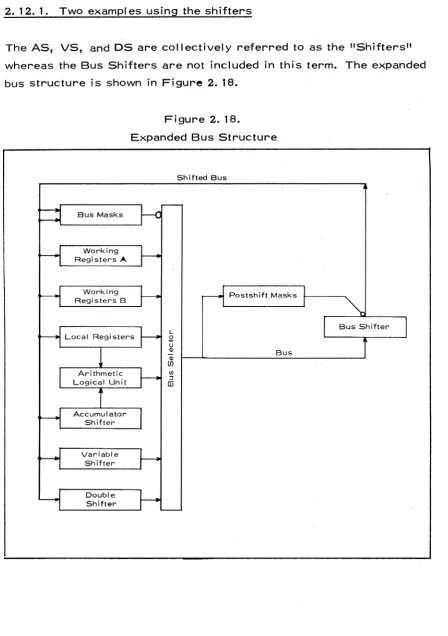
Let us now expand the initial bus structure given in Figure 2.4. by adding the Bus Masks, BM, as shown in Figure 2.8.
Figure 2.8.
Expanded Bus Structure Shifted Bus
Bus Masks
Working Registers A
Working Registers B
The BM allow one to specify wh ich bi ts of the SOURCE (i. e., the parti-cuI ar input to the bus sel ector wh ich has been sel ected for bus trans-port) are actually to be transported. A mask is a string of 16-bits. If bit i (05:i5:15) of a mask is a 1, then bit i of the SOURCE is to be trans-mitted; if bit i of the mask is a 0, then the value
°
is to be transmitted. Since the BM are not an input to the bus sel ector but affect the trans-mi ssion of the SOURCE, they are shown connected to the bus sel ector with the symbol o(which we will interpret to mean "mask") and not by the symbol ) (which means "input"). WARNING!l! When theBus-mask is loaded it is the inverted SB which is, loaded into BM •
The SOURCE is masked during every bus transport by the mask which is specified to be
where
MA
V MBMA
=
an el ement of a 16-bit wide, 16 el ement RG call ed the Mask A regi sters,MB = an el ement of a 16-bit wide, 16 el ement RG call ed the Mask B registers,
v
=
logical Iljnclusive orll.MA and MB are shown in Fi gure 2.9. Upon dead start, the system is
5G 56 00
eM Sel.
Figure 2.9.
Bus Masks, MA and MB
L +1 -1 C
5B(0:15)
Bus Mask Registers
MA
Bus Mask Registers
MB
Bus Sel ector
MB
such that the llno mask ll ,
i.
e., 15 II s, is in regi ster 0 of MA and the llbus cl ear mask ll , i. e., 16 O's, is in register 1 of MA. We wi II assume this to be the case throughout normal operation of the system. One canthen look upon the pointer MAP as a switch for the use of the bus masks: If MAP
=
0 then the BUS is not masked, if MAP=
1 then the BUS is masked by the mask specified by MB. This is, of cource, not the only interpretation of the use of the BM but it is a convenient one and one which we will normally employ unless otherwise stated.As an example, with no sensible applications, assume we are represen-ting very small floarepresen-ting point numbers in the following sign magnitude format,
b~b!xponentlll~019 coeffi~ient
01l
4sign of coefficientsi gn of exponent
Suppose the. following 4 masks are available in the first 4 registers of MB.
MBO 1 0
o :
MB1 0 1 f---tl 0 ~
.0 .
MB2 0 ~
.0
1
04
to
MB3 0
•
•
01 4
.1
i15 14 10 9 o
The following code will decompose a floating point number found in the register of WA pointed to by WAP and store the information as follows,
1)
sign of the exponent in bit 15 of WBO 2) magnitude of the exponent in WB1(15:12) 3) sign of coefficient in bit 15 of WB2MAPC.
MAP+1, MBPC, WBPC. WB:=WA MBP+1, WBP+1.
WB:=WA, +- MBP+1, WBP+1. WB:=WA, +- 5 ; MBP+1, WBP+1.
WB:=WA, +- 6 ;
•
It is suggested by this example that when one is decomposing formatted information (e. g., a virtual machine instruction) one may wish to co-ordinate the use of the BS with the use of the BM. Let us therefore suppose the sh ift constants 0, 15, 11, and 10 to be stored in the fi rst 4 registers of the BSSG. The above decomposition and storage could be written as the following 3 microoperations:
; CA:=3, MAPC, BSS:=BSSG. ; BSPC, WBPC, MBPC, MAP+1.
WB:=WA ; BSP+1, WBP+1, MBP+1, CA-l; if CA ; BSS:=CM.
lc
1_,vi
then HERE el se HERE0\(.
•
The MA Pointer (MAP) and the MB Pointer (MBP) both of which were used in the above examples are loadable either separately or together; thus we can execute the microoperations
MAP:=CMI
001
SBI SG, MBP:=CMI001
SBI SG, or MAP, MBP:=CMI001
5BI SG .The name of the SG associated with the BM is the Bus Mask Pointer (BMP) Standard Group. The following table I ists the microoperations associated with MA, MB, and BMP.
Table 2.6.
Microoperations for control of the BM
MAP+l
MAP-l
MAPC
MAP:=CM I 00 I SB I SG
MBP+l
MBP-l
MBPC
MBP:=CMI 001 SBI SG
MAP, MBP:=CMI
001
SBI SGBMP:=SB
BMPP:=CMI
001
BMPsll BMPS2BMPP+l
BMPP-l
BMPPC
BMPsl:=CMI 001 BMPsll BMPS2
BMPS2:=BMPP
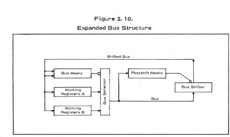
2.7. Postshift Masks
The Bus Masks, as described in the previous section, are appl ied to
the SOURCE as it is gated onto the BUS and thus before the SOURCE
is shifted in the BS. There is also a possibility of masking the SOURCE
after it has been shifted by using the Postshift Masks, PM, as shown in
Fi gure 2. 10.
4i$Wvl\i.Ii.tiih~htli<~-Figure 2. 10.
Expanded Bus Structure
Bus Masks
Working Registers A
Working Registers B
L
£
u III III
(/)
til :J
en
Shifted Bus
Postshift Masks I---..
Bus
One of the purposes of the Av1 is to appl y a mask to the output of the BS which wi II mask off the unwanted IIcycl ic" bi ts and repl ace them wi th 0' s thereby simul ating a logical shift. As an exampl e, if the bus transport
WB:=WA, ... 2
is executed with the postshift mask
l~14
.1~~ol
applied to the output of the BS, then we have taken a WA register, shif-ted it 2 bits left logical, and stored it in a WB register. Similarly, the bus transport
WB:=WA, -+ 6
wi th the mask
0000001 4 - - -
~-ll
[image:33.597.71.528.72.345.2]applied to the output of the BS means a WA register is shifted 6 bits right logical and then stored in a WB register. The output of the BS is masked during every bus transport by the mask which is specified to be
where,
PAY PG
PA
=
an element of a 16 bit wide, 16 element RG called the Postshift Mask A registers, PG=
a functional unit called the Postshift maskGenerator,
V logical "inclusive or".
PA and PG are shown in Figure 2. 11. This is quite similar to the BM where PG now takes the pi ace of MB.
WARNING!!! As with the BM, when PA is loaded from the bus, it is the
inve'~ted bus which is loaded.
CM
5G 58
00
CM
L +1-1 C
Figure 2. 11.
Postshift Masks, PA and PG
Sel.
8U5(0: 15)
eM 00 Undef SG
Postshift
Mask Registers
PA
Post shift Mask Generator, PG
Bus Shifter
The PG is a 32 word ROM which can be addressed through PGS. The contents of the ROM is
Table 2.7.
Tabl e representing the READ-ONL Y-MEMORY containing the 32 Masks for the PG
---~I---I
1
PG-DATA
I
MASK SELECTED IN
I
l s n s 1 51 DEC elNARY I
POSTSHIFT MASK GENERATOR
1
1----1---1---1
1
o I 00000 I 1 1 1 1 1 1 1 1 1 1 1 1 1 1 1 1
I...
PG.-.O, PG.O1
1 I 00001 1 o 1 1 1 1 1 1 1 1 1 1 1 1 1 1 1 I
1
2 I 00010 1 0 o 1 1 1 1 1 1 1 1 1 1 1 1 1 1 I
1
3 I 00011 1 0 0 0 1 1 1 1 1 1 1 1 1 1 1 1 1 1
I
4 I 00100 I 0 0 0 0 1 1 1 1 1 1 1 1 1 1 1 1 1
1
5 1 00101 1 o a 0 0 o 1 1 1 1 1 1 1 1 1 1 1 1
I
6 I 00110 I o 0 o 0 o 011 1 1 1 1 1 1 1 1 I
1
7 I 00111 1 0 0 0 0 o 0 0 1 1 1 1 1 1 1 1 1 I \
PG-m1
8 I 01000 I 0 0 0 0 o 0 0 0 1 1 1 1 1 1 1 1 I
I
9 1 01001 1 o 0 o 0 o 0 0 0 0 1 1 1 1 1 1 1 1
1 10 1 01010 1 o 0 0 0 o 0 0 0 0 0 1 1 1 1 1 1 I
1 11 1 01011 1 0 0 0 0 o 0 0 0 0 0 0 1 1 1 1 1 1
1 12 1 01100 I o 0 o 0 o 0 0 0 o 0 001 1 1 1 1
1 13 I 01101 1 0 0 o 0 o 0 0 0 0 0 0 0 0 1 1 1 1
1 14 I 01110 1 o 0 o 0 o 0 0 0 0 0 0 0 0 0 1 1 1
1 15 I 01111 1 0 0 0 0 o 0 0 0 0 0 0 0 0 0 0 1
~1 16 I 10000 1 o 0 o 0 o a 0 0 o 0 000 0 001
PG .... 16, PG.161 17 I 10001 I 1 0 o 0 o 0 0 0 0 0 0 0 0 0 0 0 {
1 18 I 10010 I 1 1 0 0 o 0 0 0 0 0 000 0 001
1 19 1 10011 1 1 1 1 0 0 0 0 0 0 0 0 o 0 o 0 0 I
1 20 1 10100 I 1 1 1 1 o 0 0 0 0 0 000 0 0 0 1
1 21 I 10101 1 1 1 1 1 1 0 0 0 000 0 0 0 0 0 I
I 22 I 10110 1 1 1 1 1 1 1 0 0 o 0 000 000 1
1 23 I 10111 1 1 1 1 1 1 1 1 0 0 0 0 0 0 0 0 0 1
I 24 1 11000 1 1 1 1 1 1 1 1 1 0 0 0 0 0 0 0 0 1
>
PG .. n1 25 I 11001 1 1 1 1 1 1 1 1 1 1 0 0 0 0 0 0 0 1
1 26 I 11010 1 1 1 1 1 1 1 1 1 1 1 0 000 001
1 27 1 11011 1 1 1 1 1 1 1 1 1 1 1 1 0 0 000 1
1 28 I 11100 1 1 1 1 1 1 1 1 1 1 1 1 1 0 000 I
1 29 1 11101 I 1 1 1 1 1 1 1 1 1 1 1 1 1 0 0 0 I
1 30 1 11110 1 1 1 1 1 1 1 1 1 1 1 1 1 1 1 0 0 1
I 31 1 11111 I 1 1 1 1 1 1 1 1 1 1 1 1 1 1 1 0
~1----1---1---1
The PG can generate the 32 masks required to view the BS as both a logical and cycl ic shifter. As is seen from Figure 2. 11. the postshift mask generation data can come from oneof three sources, eM\ OD
I
SG.bI,';-Which particular source is to be used as data for the mask generation is determined by the contents of a 2-bit Postshift mask Generator Selec-tion register (PGS) as shown in this figure and in Table 2.8. below.
Table 2.8.
Source of Data for Postshift Mask Generation
Contents of PGS Source of DATA
00 CM
01 OD
10 (undef)*
11 SG
- - -
-"---If, what we will assume as standard, the PGS has been set to point to the CM as the data source, then the PG data are specified in the "rr.i-crooperations and data" field of the microinstruction in the following symbol ic way,
where,
PG "arrow" n
n = the number of 0' s to be generated and the "arrow"
( .... \-+) indicates from which di rection they shaul d be
generated; 0 ~ n ~ 16.
Thus, the previous two exampl es could have been written (assuming PGS and BSS points to the CM as the data sources).
WB:=WA, .... 2; PG+-2 WB:=WA, -7 6;' PG-76
Upon dead start, the system is sU,ch that the mask of all l's is in regis-ter 0 of PA, and the mask of all O's is in regisregis-ter 1 of PA. This is identical to the situation in MA. We will assume this to be the case
*) At the moment undefined
throughout normal operation of the system. One can then look upon the pointer PAP as a swi tch for the use of the Postshift mask Generator: if PAP = 0 then the mask generator is not used, if PAP = 1 then the postshift mask which is to be applied will be that generated by the mask generator. This is, of course, not the only interpretation of the use of the postshift masks, but it is a convenient one and one which we shall normally employ unless otherwise stated.
Table 2.9. is a list of the microoperations associated with the PM. The first half of this table deals with PA. The second half of this table deals with the PG. The name of the SG associated with the PG control is the Postshift Mask Generator SG (PGSG). Note, the name of the SG associated with the PA pointer is the Postshift AB Pointer (PABP). It is not di scussed here but in Section 2.28.
Table 2.9.
Microoperations for the control of the PM
Operations associated with PA PA :=BUS
PAP:=CM 100
I
SB I SG PAP +1PAP -1 PAPC
Operations associated with PG and PGSG PGS:=CM
PGS +1 PGS -1 PGSG:=SB
PGP. :=CM 100 I PGS 1 IPGS2 PGP+1
PGP -1 PGPC
PGS 1 :=CM I
00
I PGS 1 I PGS2 PGS2:=PGP~~~::-~-.~_~~~-Let us extend the example of Section 2.5. in which we emulated a virtual machine instruction which performed a register to register transfer com-bined with left/rigth cycl ic shifting. As shown below, if we use the PG we can execute an instruction which will take a given WB register (WB Adr), shift it left/right logical or cyclic (Shift & Mask Data), and then store it in a WA register (WA Adr). If the data for the instruction is in the current WB register pointed at by WBP in the form
I
WBP -7 WB Adr WA Adr I
15
e
7 010 .... 0
Mask LshiftData Data WBP+l -7
15 11 10 4,3 0
a possibl e code sequence woul d be:
WB, WB, -74 WB WB
WAP:=SB, WBP+l. PG SG:=SB.
BSSG:=SB, WBP-l. WBP:=SB, WBPS:=WBP. PAP+l, PGS:= SG-.
If
SS: ':
Sc;. WA:=WB;r- ;~y
WB~_:.:=.YV6PSJ
..!*
-..
~.".~-.. ' " ~...-""~" , -'.
~,,~-; pAPC./ PGS:= -,---.-'''~<,." .... ''
eM.
~s
S""
en
-Note well, there are two important assumptions in this example. The first is that MAP = 0 upon entry to this code,
i.
e., a bus mask is not appl ied to the source, and the second is that PAP = 0 upon entry to this code,i.
e., no postshift masking occurs. Indeed, we will make these assumptions in all examples which follow (unl ess stated expl icitl y other-wise). They can be summarized as follows: bus transport normally oc-curs in an unmasked fashion; if a particul ar code segment requi res the use of am asking facility it is responsible for leaving the system in this normal state after such masking occurs.2.8. The Arithmetical and Logical Unit
We wi II now a:ld additional computational capabil ity to the bus structure in addition to the shifting and masking al ready encountered by introdu-cing the Arithmetical and Logical Unit (AL). The AL, shown in Figure 2.12., is a functional unit with 2 inputs which, for the moment we will call AandB.
Figure 2. 12.
Arithmetical Logical Unit, AL
Sel. Bus Selector
6 bits are required to control the AL: 5 bits to select one of the 32 ope-rations I isted in Tabl e 2.10. which this unit can execute on A and B and 1 bit which specifies the carry-in bit into the AL for any arithmetic operations.
~4-r:-~~iai.-~~~::~1..}-l't~:~-:--:--Table 2.10.
AL Functions
ARITHMETIC
A
AVB
AVB
minus 1
*
A
+
(MB)(AVB)
+
(MB)A-B-1
(MB)-l
A
+
(MB)A+B
AVB
+
(MB)(MB)-l
A+A
(AVB)+A
(AVB)+A
A-l
LOGICAL
A
A!\B
A!\B
all O's
AVB
B
AfB
A!\B
AVB
A=B
B
A!\B
all l's
AVB
AVB
A
*
in 2's complement; the arithmetic operations are shown with thecarry-in set to
o.
If the carry-in is 1, then the AL Function is F+1 where Fis the specified arithmetic function. The logical functions are not
affec-ted by the carry-in.
The 6 control bits which specify the current operation for the AL are the contents of the AL Function and Carry-in register, ALF, which can be loaded, ALF:=CMlooISBISG, or set to the arithmetic addition operation A + B and other standard settings. The SG associated with the ALF
is called the AL Standard Group (ALSG). The microoperations associated with the ALare given in table 2. 11.
Table 2.
11-Microoperations for control of the AL
ALF:=CM 100 I SB I SG SET ALF +
SET ALF-SET ALF B SET ALF A - 1 ALSG:=SB
ALP:=CMIOOIALS1IALS2 ALP +1
ALP -1 ALPC
ALS 1 :=CM 100 I ALS 1 I ALS2 ALS2:=ALP
If the ALF is to be loaded with an operation specification from the CM, we will note this symbolically merely by writing the required function in the symbol ic form which appears in Tabl e 2.10. in the ALF assignment statement, i. e. ,
ALF:=A + B ALF:=A 1\ B etc.
The AL is always running. If the ALF is changed in a microinstruction, then the result of the newly computed function is available for bus
port in the very next microoperation. Thus the microinstructions ALF:=all 1 s, PAP +1.
WA:=AL; PG ~ 9, PAP -1 .
•
will put a string of 71's in the WA register pointed to by WAP. The 1's will be least significant bits, bo, justified.
There are many testable conditions concerning the operation of the AL. A few of these are
Symbol ic Notation Condition
AL resul t of AL operation all 1's
AL(O) bit 0 of the result of the AL operation AL( 15) bit 15 of the resul t of the AL operation ALOV AI overflow (equivalent to a carry-out
during addition and a borrow-in during subtraction)
Before giving examples of the control of the AL let us first discuss the nature of its inputs, A and S.
2.9. The Local Registers
The Local Registers, LR, serve as the A input to the AL in the context of the AL Functions shown in Table 2.10. The LR, shown in Figure 2. 13, are 4 16-bit wide registers which have independent input and output pointers. The input pointer, LRIP, points to a LR which can be used as a SO for the current bus transport. The output pointer, LROP, points to a LR which can be used as either the A input to the AL or as the SOURCE for the current bus transport.
Figure 2. 13. Local Regi sters, LR
L +1 -1 C L +1 -1 C
OS(v:v+ll
BO Load
LRO
LR1
1--...----' .... Bus Sel ector
LR2
A Input of AL
LR3 o
Both the LR input pointer, LRIP, and the LR output pointer, LROP, are incrementable, decrementable, clearable, and loadable with two bits from the Doubl e Shifter, DS(V:V+l) , see Section 2. 12. The uti I ity of this last feature will be demonstrated with examples when the Double Shifter is introduced. Tabl e 2. 12. gives the microoperations associated with the control of the LR.
Table 2.12.
Microoperations for control of the LR
LRIPC
LRIP + 1
LRIP - 1
LRI P:=DS(V:V+1)
LROPC
LROP + 1
LROP - 1
LROP:=DS(V:V+1 )
LRPC
LRP + 1
LRP - 1
LRP:=DS(V:V+1 )
The last four microoperations allow for the clearing, incrementing,
decrementing, and loading of both the IP and the OP simul taneousl y.
2. 10. The Accumul ator Shifter
The Accumulator Shifter, AS, serves as the B input to the AL in the
context of the AL functions shown in Table 2.10. The AS can serve as
a bus DESTINATION; but to be read, its contents must be gated through
the AL with the ALF set to
B.
The AS, shown in Figure 2. 14., is a1-bit shifter which can shift left, shift right, be loaded, or remain idle
during the execution of any given microinstruction.
Figure 2. 14.
Accumulator Shifter, AS
eM OD 58 SG
Sel.
L C Load/Shift L C
Source AS(15) AS(O)
nco Input Input
Q Q 0
1 1 1
2 I AS(O) AS(15)
3 AS(15) BUS(15)
4 Undef SB(15)
5 DS(V+1) DS(V+1)
6 AS(V) AS(V)
7 VS(V) VS(V)
There are 2 interesting features of thi s shifter:
a) its variable width characteristic and
b) its connection to other el ements of the system.
The features are discussed in the following:
a) Although the shifter is 16-bits wide it may, in connection with eit-her the 8M or PM, be viewed as being m-bits wide (1 ~ m ~ 16). This is accompl i shed by having each of the 16 bi ts of the AS input to a sel ec-tor (I abel I ed the bo - ~5 sel ector in Fi gure 2. 14). The output of this sel ector (call ed the variabl e bit, V) can then be a possibl e input into either the I eft or right end of the shifter, depending upon what particu-lar type of shift one requires. When the AS is selected as a source for bus transport by gating it through the AL, after the desired shift
[image:45.595.99.528.50.489.2]has occurred, the bits not consi dered to be a part of the shifter must be masked off. This can be done either by using the BM or the Av1. The width of the shifter is then determined by the contents of the AS(V)
Selection register, AS(V)S, as shown in the above figure and the use of of an appropriate mask.
The AS(V)S can be loaded by the following microoperation
AS(V)s:=cMI
001
SBI SG.Thus, for exampl e, if we wi sh to consider the AS as a 12 bit I eft cyc-I ic shifter, we would execute the microoperation
AS(V)S:=ll
while making sure that AS(V) be used as the input to bit AS(O) during the shift operation. Subsequent use of the AS as a source could be ac-compani ed by use of the PG masking off bits b15 - b12 , e. g.
SET ALF B .
WA:=AL; P~4
•
b) In Figure 2. 14. it is seen that bits AS(O) and AS(15) can be filled by one ofavarietyofsourcesduringashift operation. Which source is to be used to fi II the vacated bit position is determined by the contents of the AS(O) and AS(15) source selection registers, AS(O)S and AS(15)S respectivel y. An examination of the tabl e in Figure 2. 14. shows that the AS can be considered a logical shifter, a 1 IS fill shifter, a cycl ic
shif-ter, and a right arithmetic shifter. It can al so be connected to another 1 bit shifter, call ed the vari abl e width shifter, VS, to yi eld a long vari ab-I e width shifter. ab-I t can be connected to a 2-bit shifter call ed the Ooubl e Shifter, OS, so it can be used in the merging of 2 bit streams into 1 or
the diverging of 1 bit stream into 2. I t can al so be connected to the BUS and SB. These I atter input is of an experimental nature and uses wi II be
demonstrated in later exampl es.
-Thus to use the AS, one must load the AS(V)S to set the width of the shifter and must load either the AS(O)S or AS(lS)S to point to the source to be used as the input into the vacated bit position,
i.
e., one must set what the type of shift is, e. g., logical, l's fill, long, etc. That both of these operations need not be done each time the shifter is used, but only when one is "changing" the width or type of shifter is obvious. Table 2. 13. I ists the microoperations associated with the control of the AS. Note the AS can be set to a logical I eft, ASLL, or logical right, ASLR, shift.Table 2. 13.
Microoperations for control of the AS
AS(O)S :=cMloDISBISG AS( lS)S:=CM I OD I SB I SG AS(V)S :=CM I OD I SB I SG ASLL ( == AS(O)SC) ASLR ( == AS( lS)SC) AS(V)SC
AS(V)S+l AS(V)S-l
There are 2 bits in each microinstruction which control the operation of the AS: shift left, AS<-, shift right, A5-?, load, i. e., AS:=SB(O:lS), or be idle. When the AS is to be shifted, the operation is put in the
"microoperation and data" fi el d of the microinstruction; when the AS is to be loaded, the operation is specified in the "bus transport" field of the microinstruction. As an example, the microinstruction
WA:=AL; AS<- .
stores the output of the AL in a WA register and then shifts the AS I eft, while the microinstruction
LR, AS:=WB; WBP + 1 •
stores a WB in both the AS and a LR and then increments the WB poin-ter. If the AS is not employed during a given microinstruction, it does not appear in the specification of that microinstruction.
Having introduced the AL and its inputs, LR and AS, we now have knowl edge of the expanded bus structure as shown in Fi gure 2. 1
S.
Bus Masks
Working Registers A
Working Register B
Fi gure 2. 1
S.
Expanded Bus Structure
'-2 u
Q) Q)
Ul
Ul ::J aJ
Postshift Masks
Let us now give a few exampl es using these resources to demonstrate the use of their associated microoperations.
;'-';i'<!--.:ilt~.~~;=;'~5K-_---;-Example 1
Let us consider WA as a stack as shown below
WA
Stack pointer • op
(WAP)
a
b
15 0
We wish to take two operands, a and b, and an arithmetical or logical operator, op, from the stack and pi ace a op b on the new top of stack. The following microinstruction sequence does this.
WA ALF:=SB, WAP - 1, LRPC. LR :=WA; WAP -
1 •
AS:=WA. WA:=AL.
Example 2
Let us again consider WA as a stack.
WA
Stack pointer • shiftspec
(WAP)
a
15 0
We wish to treat the AS as a I eft shifter whose characteri stics are gi-ven by shiftspec. We wish to shift a n-times and return the result to the new top of stack after removing shiftspec and a. Let us assume shiftspec to have the following format.
where
11:-~-~J~~k7j:Width
312
typeoI
type = encoding found in the table of Figure 2.14 for logical, cycl ic, etc. shift,
width = width of shifter - 1, 1 ::; width of shifter::; 16 pgmsk = PG mask specification,
n = number of shifts - 1, 1::; number of shifts::; 16
The following microinstructions execute the desired operation.
WA AS(O)S:=SB.
WA, -7 3; AS(V)S:=SB. WA, -7
7;
PGSG:=SB.WA, -712; CA:=SB, WAP + 1.
/. AS :=WA; PGS:=SG, PAP + 1, SET ALF B.
~"
A9- ; if CA then HERE+l else HERE.
cg
-I
WA:=AL; PAP-1, PGS:=CM.
•
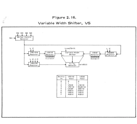
2. 11. The Variable Width Shifter
The Variable Width Shifter, VS, is a shifter functionally identical to the AS. The reason one is called the Accumulator Shifter is that not only does it serve as an input to the AL, but al so it wi II serve as the accumulator required in the real ization of the basic arithmetic opera-tions (e. g. mul tipl ication). The VS can be a SOURCE or DESTINA-TION for a bus transport. It is shown in Figure 2. 16.
~.!,~".,,~_;-:-;;-~:~-~;\.f-_~",,_'-<-_.;_~~~~iii*~-ii"_ailliifb"iJil'_'>~r.~-Fi gure 2. 16.
-i. ~
Variable Width Shifter, VS
eM 00 58 SG
Sel.
Source VS(1S) vs(o)
no. Input Input
a a a
1 1 1
2 VS(O) VS(1S)
3 VS(1S) BUS(14)
4 Undef SB(14)
I
5 DS(V) DS(V)
6 VS(V) VS(V)
7 AS(V) AS(V)
The microoperations associated with the VS are identical to those as-sociated with the AS and are I isted below in Tabl e 2. 14.
Table 2. 14.
Microoperations for control of the VS
VS(O)S :=CM\
ODI s81
SG VS( 1 S)S:=CM 100I
S8I
SG VS(V)S :=CMI 001 S8 I SG VSLL ( == VS(O)SC) VSLR ( == VS( 1 5) SC) VS(V)SCVS(V)S
+
VS(V)S [image:51.598.91.531.55.455.2]--->---:"~-.I.'~""'~NF'~ti~<.fo~~':-One of the important features of the AS and VS, as seen from the tabl es in Figures 2. 14. and 2. 16., is that they can be connected together. Thi s allows, for example, the AS and VS to be viewed as a "long" shifter when coupled together. The microinstructions,
AS( 15):=7, VS( 15) :=7.
AS(V)SC, VS(V)SC.
•
connect the AS and VS together so that they can be viewed as a right cycl ic 32-bit shifter as shown below.
r--~AS
-oH;---VS---:
1
Just as with the AS, there are 2 bits in each microinstruction which control the operation of the VS: shift I eft, VS ... , shift right, VS-7, load, i.e., VS:=SB(0:15), or remain idle.
Assuming the previous AS/VS connection has been made, subsequent execution of the microoperations
AS-7, VS-7
shifts this 32-bit shifter 1 bit right cyclic. Other "long shifters", e. g. left logical, right logical, right arithmetic, etc., result from appro-priate set up sequences.
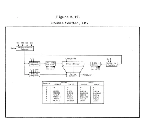
2. 12. Doubl e Shifter
The Double Shifter, DS, is a shifter with functional characteristics similar to those of the AS and VS, except that it shifts 2 bits at a time and not 1. Bits DS(O) and DS(
1)
require input during a I eft shift and DS(14) and DS(15) require input during a right shift. The DS is shownin Figure 2.17. The DS can be a SOURCE for or a DESTINATION of a bus transport •
Figure 2. 17. Double Shifter, OS
eM 00 SB SG
Source Inputs Inputs
05(15) 05(14) 05(1) 05(0)
0 0 0 0 0
1 1 1 1 1
2 05(1) 05(0) 05(15) 05(14)
3 05(15) 05(15) BUS(15) BUS(14)
4 Undef Undef SB(15) SB(14)
5 OS(V+I) OS(V) OS(V+l) DS(V)
6 AS(V) VS(V) AS(V) VS(V)
7 BUS(I) BUS(O) Undef Undcf
[image:53.598.80.539.55.445.2]
-The microoperations which are associated with the OS are directly comparabl e to those for the AS or VS and are shown in Tabl e 2. 15.
Table 2.15.
Microoperations for control of the OS
DS(O:l)S :=cMI 001 s81 SG OS( 14: 15)S:=CM I 00 I S8 I SG DS(V)S :=cMI ODI s81 SG DSLL
DSLR OS(V)SC DS(V)S + 1 DS(V)S - 1
(== DS(O:1)SC)
( == DS(14:15)SC)
The bo - ~5 selector specifies two bits OS(V:V+1) as output, these may be used in coupling the shifters, or as input to the LRIP and LROP-pointers.
There are 2 bits in each microinstruction which control the operation of the OS: shift left, OS<-, shift right, OS~