Effective Electrode Length Enhances Electrical
Activation of Nanowire Networks: Experiment and
Simulation
Jessamyn A. Fairfield†¶, Carlos Ritter‡¶, Allen T. Bellew†¶, Eoin K. McCarthy†¶, Mauro S. Ferreira‡¶, John J. Boland*†¶
†School of Chemistry, Trinity College Dublin, Dublin 2, Ireland.
‡School of Physics, Trinity College Dublin, Dublin 2, Ireland.
¶Center for Research on Adaptive Nanostructures and Nanodevices, Trinity College Dublin, Dublin 2, Ireland.
KEYWORDS. Nanowire, network, sheet resistance, activation, conductivity, tunable.
ABSTRACT. Networks comprised of randomly oriented overlapping nanowires offer the
possibility of simple fabrication on a variety of substrates, in contrast with the precise placement required for devices with single or aligned nanowires. Metal nanowires typically have a coating of surfactant or oxide that prevents aggregation, but also prevents electrical connection.
comprise the network. We show through both simulation and experiment that electrical stimulation, microstructured electrode geometry, and feature scaling can all be used to manipulate the connectivity and thus, electrical conductivity of networks of silver nanowires with a non-conducting polymer coating. More generally, these results describe a strategy to integrate nanomaterials into controllable, adaptive macroscale materials.
Randomly oriented nanowire networks have the potential to combine novel electronic
properties with extreme ease of fabrication.1, 2 Currently, metallic nanowire networks are being investigated as next-generation transparent conductors,3, 4 artificial skins,5-7 and flexible
optoelectronic devices.8-10 However, to build reliable materials and devices, it is necessary to be able to tune the sheet resistance, and hence the connectivity between the wires that comprise these networks. Since most wires are coated with an oxide or some form of surface
properties. However, for large scale nanowire networks, prohibitively high voltages can be required to activate this memristive behavior,2, 15 so that the reduction of the activation voltage is an important challenge in realizing large area materials and devices.
in these networks,2 we can predict the effects of microstructuring electrodes on the activation voltage and sheet resistance of networks, confirmed here through experimental data. We also discover the importance of electrode length for nanowire networks, and elucidate the role of the overall distributions of junction properties in determining network behavior.
Results and Discussion
Experiment. Silver nanowire network devices were fabricated by spray deposition25 and evaporation of metal electrodes (see Methods). A transmission electron micrograph of the surface of one silver nanowire is shown in Figure 1(a). The nanowires had mean diameters of 85 ± 10 nm and lengths of 7.5 ± 2 m, as seen in Figure 1(b), and a 1-2 nm thick coating of
polyvinylpyrrolidone (PVP) forming the surface layer, visible in Figure 1(a), which can be non-conducting or non-conducting depending on the electrical history of the device. Devices were then contacted by probes for electrical measurements, as seen in Figure 2(a) where a nanowire network is bounded by two serrated metal electrodes whose tip-to-tip separation is 200 m, defining an active network area of 200 m by 200 m. Networks are electrically activated by setting the compliance current to either 10 A or 120 nA depending on device size, then
by 50 m nanowire network was contacted either by two flat electrodes, a single flat electrode and a pointed electrode, a single flat electrode and a single serrated electrode, and two serrated electrodes, as shown schematically in Figure 2(b).
Current-voltage (I-V) measurements were performed by increasing the current compliance to 5 mA after activation, and the voltage is swept from 0 to +Vmax to 0 to -Vmax. Initially Vmax is set to Von. Then the maximum voltage is gradually increased, to activate additional current paths, evolving the network. Sample activation and evolution I-V curves for a device, as well as an electron micrograph of the nanowire network for the case of point and bar electrodes separated by 50 m, are shown in Figure 3. Sheet resistance is measured immediately after device
activation when current is stable, and these measurements are performed over a sufficiently low voltage range so that additional evolution does not occur and the resistance is stable. Based on four-probe measurements, for a 50 m by 50 m nanowire network we would expect ~65% of the resistance to come from the contact between the electrodes and the nanowire network, with the remaining resistance coming from the nanowires and interwire junctions. All four geometries were then compared by examining the Von and sheet resistance at Von of each device.
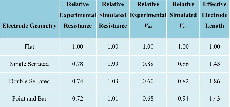
devices from multiple chips are tabulated in Table 1. Each number is the ratio between the performance values of devices with more complex electrode geometries (one electrode serrated, both electrodes serrated, or one electrode pointed) and the performance values of a flat square electrode shape. The tabulated data show that, on average, serrations strongly reduce Von and sheet resistance. Passive voltage contrast imaging in a scanning electron microscope shows that the serrations or points on the electrode are preferentially activated as in Figure 4, where part (a) shows topography, and part (b) shows passive voltage contrast imaging of connected nanowires. Note in (b) the darker, less visible regions of the network form a conducting path between the electrodes, whereas the brighter wires are disconnected from this path but can become connected after additional electrical stressing.2 The data from the point and bar geometry show the largest scatter, which we suggest is due to the increased importance of a single area of the nanowire network (i.e. at the point), compared to serrations which have several possible nucleation sites for conductivity pathways. The large numbers of devices measured on two different chips
rectangular electrodes compared to the flat square case strongly suggesting that the increased electrode length is likely the main factor in reducing the sheet resistance.
Simulation. Whilst we can propose qualitative explanations for the geometric scaling effects on the electrical behavior, we also performed simulations of static electric properties to
corroborate these results and obtain physical insights about the nanowire network properties and their dependence on junction properties. In our model of network activation, the nanowires are represented by one-dimensional rods lying on a two-dimensional plane.21 Their length lw, center point position (xc,yc) and angle θ are randomly generated in order to create randomly-oriented networks. When a bias voltage V is applied across the network, individual voltage drops 𝑣𝑖 occur across each junction i, with the wires treated as equipotential line segments. The inter-nanowire junctions can be either non-activated, if the voltage drop 𝑣𝑖 across the junction is not strong
enough to modify the dielectric coating, or activated, if 𝑣𝑖 ≥ 𝑣𝑏𝑖, where 𝑣𝑏𝑖 is the voltage drop across junction i above which the dielectric is modified so that a conducting path forms between the nanowires. The non-activated junctions can be described as capacitors, building up charge on both sides of the dielectric coating, and the activated junctions can be described as resistors, with resistance determined by the conducting path that links the metallic cores. In fact, we consider the junction resistances to be the only source of resistance in the model, thus the resistance of the junctions dominates the overall network resistance. In this representation, the junction break voltage 𝑣𝑏𝑖 represents the junction voltage above which the junction behavior switches from capacitive to resistive. Therefore, as one increases the applied voltage, the system reaches
activation (V = Von) when there is a percolating path of resistors. The physical characterization of the network is based on individual wire lengths and network junction properties—resistances 𝑅𝑖,
experimental measurements on individual junctions. The electrical properties of the nanowire networks can then be described using Ohm's law and Kirchoff's circuit laws, similar to the approach developed by Cserti.26 These laws can be summarized in the following equation:
𝐼𝑗 = ∑ 𝑈𝑗𝑅−𝑈𝑙 𝑗𝑙
<𝑙,𝑗> , (1)
where Uj is the electrostatic potential at wire j, Rjl is the resistance at the junction between wires j and l, Ij is the current going in or coming out of wire j and the sum is on l, where l is the first nearest neighbor (FNN) of j. This equation can be written in matrix notation as
𝐌𝑅𝐔 = 𝐈 , (2)
where U contains the potential at each wire and I represents the current that goes in and out of each element (nanowire or electrode) of the network circuit. I is a vector with only two non-zero values (i and –i), corresponding to the source and drain elements, and zero values for all the remaining wires. Furthermore, the matrix MR, which contains the system connectivity, is defined as
𝑀𝑅𝑗𝑙 = {
∑ 𝑅𝑗𝑘−1
<𝑘,𝑗> , if 𝑗 = 𝑙 −𝑅𝑗𝑙−1, if 𝑗 and 𝑙 are FNN
0, if otherwise
. (3)
After solving equation (2) for U, one can obtain the system conductance from
𝛤𝐿𝑅 = 𝑅𝐿𝑅−1= (𝑈𝐿−𝑈𝑅
𝑖 )
−1
, (4)
Before calculating the capacitance, one must determine which junctions are activated by solving a matrix equation based on the definition of the capacitance, C = Q/V,
𝐌𝐶𝐔 = 𝐐 , (5)
where MC has the same form as MR exchanging 𝑅𝑗𝑙−1 for 𝐶
𝑗𝑙. Q represents the charge that builds
up on the system due to the applied voltage V. If one solves this equation for U, the vi across any junction can be determined for any voltage applied to the network. Therefore, only the activated junctions will be considered when determining MR.
In the present model, we add charge accumulation at the sharp edges of the contacts, as a proxy for the electric field enhancement due to the electrode geometry. The aim is to understand how the enhancement in the network connectivity due to this effect compares to the enhancement that originates from the increase of the electrodes effective length. The distributions of junction resistance, junction capacitance, junction activation voltage, and nanowire length were generated
from experimental measurements on single nanowire-nanowire junctions, as well as the
experimentally measured nanowire density and network size. (See the Supporting Information
for the junction property distributions used.) We found gamma distributions based around experimental mean values to give the best agreement between experimental and theoretical
results, reasonable given that the experimental wire length distribution was itself closest to a
gamma distribution. Changing the individual nanowire property distributions affected the final
Von and sheet resistance, contrary to previous simulations of one-dimensional memristive
networks where the overall network behavior had limited dependence on component memristor
Figure 5 shows the connectivity paths that form as the simulated voltage across the network is increased. There is a clear difference between the activation patterns in the four cases, with some paths seeded by serrations and more paths coming from microstructured electrodes. In our simulations, the change in Von and sheet resistance is mainly due to the increase in electrode
length, and our results show that charge accumulation and field enhancement plays only a very minor role in the improvement of the connectivity on the length scales employed in the present experiments. Even increasing the tip angle to 30°, which should enhance the electric field further, had a negligible effect on Von, implying that the most important change in connectivity comes from differences in the effective electrode length between the four cases presented. The left panels of Figure 5 show the wires that form conducting paths to the left (in green) and right (in red) electrodes when the network is under an applied voltage of 0.66Von, for various electrode geometries. Under these conditions there is no continuous conducting path between the
electrodes. The center panels show the wires (in blue) which have just formed conducting paths connecting both electrodes, meaning that the system has achieved a percolating path of resistors and the conductance becomes non-zero, at V = Von. The right panels show the evolution in the conducting paths (in blue) in the network when the voltage is increased to 1.33Von. The actual voltages are shown in Figure 5 for each of the four electrode configurations.
show that by increasing the network wire density for flat electrodes, the activation voltage and sheet resistance can be continuously reduced, going beyond densities that were implemented experimentally in this work, as shown in Figure 6(b). We examined other electrode geometries at various network densities and found that an increase in network wire density enhances the effect of increasing the effective electrode length, enabling easier network activation. It is worth noting, however, that increasing the network wire density reduces the system transparency which is an important issue for transparent conductor applications. Furthermore, in simulated devices whose electrode width is twice as large as the inter-electrode separation, Von is lowered by 13%
compared with the square network case, confirming our experimental measurement that increasing electrode length without electric field enhancement modifies device behavior.
the device area, and these additional paths may increase the impact of electrode microstructuring. However, in general, simulations and experiments both demonstrate that electrode geometry can be used as a handle to tune nanowire network behavior, in addition to the more obvious methods of changing the density of nanowires and the distribution of wire properties.
Conclusion
Additional refinement of the model by incorporating electric field effects within the network and nuanced evolution of junctions will assist in future combined experimental and computational work.
METHODS.
Devices were fabricated on silicon wafers coated with 300 nm of thermal silicon oxide. Silver nanowires obtained from Seashell Technologies were spray-deposited onto the substrates, using an Infinity Spray Gun mounted in a Janome JR 2300N Desktop Robot for evenly dispersed and randomly oriented sprayed networks. Electron beam evaporation was then used to deposit 5 nm of titanium as an adhesion layer, followed by 60 nm of gold, through a shadow mask to define electrical contacts. The top-contacted electrodes ensure good electrical connection to the nanowires, which were sprayed to a density of 0.3 nanowires/m2 or 85% transmittance.
Nanowire size distributions were measured by examining scanning electron micrographs by hand in ImageJ. Electrical measurements were performed by contacting the two lateral electrodes with probes connected to a computer-controlled voltage source (Keithley 2400) to record current-voltage (I-V) characteristics for each device. Transmission electron microscopy was performed on an FEI Titan, and scanning electron microscopy was performed on a Zeiss Ultra. Simulations were written in Python.
Figure 1. (a) Transmission electron micrograph showing a silver nanowire with non-conducting polymer surface coating visible. (b) Length distribution for silver nanowires used. The mean value and asymmetric shape were used as a basis for simulation nanowire length distributions.
Figure 2. (a) Scanning electron micrograph showing a 200 m silver nanowire network device between two serrated metal electrodes, contacted by two sharp probes for electrical measurement and imaging. (b) Diagram showing all of the electrode geometries explored in this study.
Electrodes can either be square and flat on all sides, or have one side serrated, or both sides serrated, or have one side come to a single point. The electrode shaping affects the total electrode length as well as the electric field strength in the device area.
Figure 4. (a) Secondary electron image showing topography of a 50 m silver nanowire network device with one serrated electrode. (b) Scanning electron micrograph with passive voltage
contrast from an in-lens detector of the same device as in (a). The device has been electrically activated and the darker nanowires are connected to ground, showing conductivity paths seeded by the serrations.
Figure 5. Simulated activation for nanowire networks with a density of 0.3 nanowires/m2 between (a) flat electrodes, (b) one flat and one serrated electrode, (c) two serrated electrodes, and (d) point and bar electrodes. The left, center and right panels show the networks at V = 0.66Von , V = Von and V = 1.33Von, respectively. The dark gray areas represent the electrodes. The red, green and blue wires belong to conducting paths to left, right and both electrodes,
respectively.
Figure 6. (a) Simulated ratio of activated junctions to total junctions fa as a function of the
applied voltage V for a 200 x 200 m network with flat electrodes (Von = 15 V) and a nanowire density of 0.3 nanowires/m2. The inset shows the same curve as the main plot for lower voltage values. (b) Simulated activation voltage Von and sheet resistance at activation Ron as a function of
wire density for the flat electrode case.
Electrode Geometry
Relative Experimental
Resistance
Relative Simulated Resistance
Relative Experimental
Von
Relative Simulated
Von
Effective Electrode
Length
Flat 1.00 1.00 1.00 1.00 1.00
Single Serrated 0.78 0.99 0.88 0.86 1.43
Double Serrated 0.74 1.03 0.60 0.82 1.86
[image:16.612.78.518.73.279.2]Point and Bar 0.72 1.01 0.68 0.94 1.43
Table 1. Comparison of experimental and simulated sheet resistance, experimental and simulated activation voltage, and electrode length for nanowire network devices with various sizes and electrode geometries. The nanowire density for all devices was 0.3 nanowires/m2. Each entry is a ratio of the change between the value for a shaped electrode and the value for a flat electrode, so that the flat electrode ratios are all 1.
ASSOCIATED CONTENT
Supporting Information. Data tables of activation voltage and sheet resistance; distributions of resistance, capacitance, and voltage break values used for junction simulations, and simulated junction activation map for a large network. This material is available free of charge via the Internet at http://pubs.acs.org.
AUTHOR INFORMATION Corresponding Author
Author Contributions
J.A.F. wrote the paper, performed the nanowire network measurements, and did the scanning electron microscopy and sample fabrication. C.R. performed network simulations and modelling. A.T.B. provided single-junction values. E.K.M. performed transmission electron microscopy. M.S.F. developed the model, and M.S.F. and J.J.B. directed the work.
Funding Sources
The authors wish to acknowledge funding from the European Research Council under Advanced Grant 321160. This publication has emanated from research supported in part by a research grant from Science Foundation Ireland (SFI) under Grant Number SFI/12/RC/2278. MSF
acknowledges financial support from the Programme for Research in Third Level Institutions
(PRTLI) and from Science Foundation Ireland (Grant No. SFI 11/ RFP.1/MTR/3083). J.A.F.
acknowledges funding from the Irish Research Council EMPOWER Fellowship, and C.R. acknowledges funding from the Brazilian National Council for Scientific and Technological Development.
ACKNOWLEDGMENT
The authors wish to thank D. Daly for assistance with passive voltage contrast imaging and for access to CRANN Advanced Microscopy Laboratory facilities.
REFERENCES
1. Madaria, A. R.; Kumar, A.; Ishikawa, F. N.; Zhou, C., Uniform, Highly Conductive, and Patterned Transparent Films of a Percolating Silver Nanowire Network on Rigid and Flexible Substrates Using a Dry Transfer Technique. Nano Res. 2010, 3, 564-573.
3. De, S.; Higgins, T. M.; Lyons, P. E.; Doherty, E. M.; Nirmalraj, P. N.; Blau, W. J.; Boland, J. J.; Coleman, J. N., Silver Nanowire Networks as Flexible, Transparent, Conducting Films: Extremely High DC to Optical Conductivity Ratios. ACS Nano 2009, 3, 1767-1774. 4. Yim, J. H.; Joe, S.-Y.; Pang, C.; Lee, K. M.; Jeong, H.; Park, J.-Y.; Ahn, Y. H.; de Mello,
J. C.; Lee, S., Fully Solution-Processed Semitransparent Organic Solar Cells with a Silver Nanowire Cathode and a Conducting Polymer Anode. ACS Nano 2014, 8, 2857-2863. 5. Boland, J. J., Flexible Electronics: Within Touch of Artificial Skin. Nat. Mater. 2010, 9,
790-792.
6. Gong, C.; Liang, J.; Hu, W.; Niu, X.; Ma, S.; Hahn, H. T.; Pei, Q., A Healable,
Semitransparent Silver Nanowire-Polymer Composite Conductor. Adv. Mater. 2013, 25, 4186-4191.
7. Takei, K.; Takahashi, T.; Ho, J. C.; Ko, H.; Gillies, A. G.; Leu, P. W.; Fearing, R. S.; Javey, A., Nanowire Active-Matrix Circuitry for Low-Voltage Macroscale Artificial Skin. Nat. Mater. 2010, 9, 821-826.
8. Lan, X.; Bai, J.; Masala, S.; Thon, S. M.; Ren, Y.; Kramer, I. J.; Hoogland, S.; Simchi, A.; Koleilat, G. I.; Paz-Soldan, D., et al., Self-Assembled, Nanowire Network Electrodes for Depleted Bulk Heterojunction Solar Cells (Adv. Mater. 12/2013). Adv. Mater. 2013, 25, 1768-1768.
9. Langley, D. P.; Giusti, G.; Lagrange, M.; Collins, R.; Jiménez, C.; Bréchet, Y.; Bellet, D., Silver Nanowire Networks: Physical Properties and Potential Integration in Solar Cells. Sol. Energ. Mat. Sol. Cells 2014, 125, 318-324.
10. Liang, J.; Li, L.; Tong, K.; Ren, Z.; Hu, W.; Niu, X.; Chen, Y.; Pei, Q., Silver Nanowire Percolation Network Soldered with Graphene Oxide at Room Temperature and Its Application for Fully Stretchable Polymer Light-Emitting Diodes. ACS Nano 2014. 11. Hu, L.; Kim, H. S.; Lee, J.-Y.; Peumans, P.; Cui, Y., Scalable Coating and Properties of
Transparent, Flexible, Silver Nanowire Electrodes. ACS Nano 2010, 4, 2955-2963. 12. Garnett, E. C.; Cai, W.; Cha, J. J.; Mahmood, F.; Connor, S. T.; Greyson Christoforo, M.;
Cui, Y.; McGehee, M. D.; Brongersma, M. L., Self-Limited Plasmonic Welding of Silver Nanowire Junctions. Nat. Mater. 2012, 11, 241-249.
13. Avizienis, A. V.; Sillin, H. O.; Martin-Olmos, C.; Shieh, H. H.; Aono, M.; Stieg, A. Z.; Gimzewski, J. K., Neuromorphic Atomic Switch Networks. PLOS ONE 2012, 7, e42772. 14. Oskoee, E. N.; Sahimi, M., Electric Currents in Networks of Interconnected Memristors.
Phys. Rev. E: Stat., Nonlinear, Soft Matter Phys. 2011, 83, 031105.
15. Yang, J. J.; Strukov, D. B.; Stewart, D. R., Memristive Devices for Computing. Nat. Nanotechnol. 2013, 8, 13-24.
16. Bellew, A. T.; Bell, A. P.; McCarthy, E. K.; Fairfield, J. A.; Boland, J. J., Programmability of Nanowire Networks. Nanoscale 2014.
17. Mutiso, R. M.; Kikkawa, J. M.; Winey, K. I., Resistive Switching in
Silver/Polystyrene/Silver Nano-Gap Devices. Appl. Phys. Lett. 2013, 103, 223302-1-5. 18. Bergin, S. M.; Chen, Y.-H.; Rathmell, A. R.; Charbonneau, P.; Li, Z.-Y.; Wiley, B. J., The
Effect of Nanowire Length and Diameter on the Properties of Transparent, Conducting Nanowire Films. Nanoscale 2012, 4, 1996-2004.
19. White, S. I.; Mutiso, R. M.; Vora, P. M.; Jahnke, D.; Hsu, S.; Kikkawa, J. M.; Li, J.; Fischer, J. E.; Winey, K. I., Electrical Percolation Behavior in Silver Nanowire–
20. Colvin, J., A New Technique to Rapidly Identify Low Level Gate Oxide Leakage in Field Effect Semiconductors Using a Scanning Electron Microscope. EOS/ESD Symp. Proc. 1990, EOS-12, 173-174.
21. Li, J.; Zhang, S.-L., Finite-Size Scaling in Stick Percolation. Phys. Rev. E: Stat., Nonlinear, Soft Matter Phys. 2009, 80, 040104.
22. Mutiso, R. M.; Sherrott, M. C.; Rathmell, A. R.; Wiley, B. J.; Winey, K. I., Integrating Simulations and Experiments To Predict Sheet Resistance and Optical Transmittance in Nanowire Films for Transparent Conductors. ACS Nano 2013, 7, 7654-7663.
23. Obukhov, S. P., Percolation in a System of Randomly Distributed Sticks. J. Phys. A: Math. Gen. 1988, 21, 3975-3978.
24. Žeželj, M.; Stanković, I., From Percolating to Dense Random Stick Networks: Conductivity Model Investigation. Phys. Rev. B 2012, 86, 134202.
25. Scardaci, V.; Coull, R.; Lyons, P. E.; Rickard, D.; Coleman, J. N., Spray Deposition of Highly Transparent, Low-Resistance Networks of Silver Nanowires over Large Areas. Small 2011, 7, 2621-2628.
26. Cserti, J.; Dávid, G.; Piróth, A., Perturbation of Infinite Networks of Resistors. Am. J. Phys. 2002, 70, 153-159.