University of Warwick institutional repository:
http://go.warwick.ac.uk/wrap
A Thesis Submitted for the Degree of PhD at the University of Warwick
http://go.warwick.ac.uk/wrap/66300
This thesis is made available online and is protected by original copyright.
Please scroll down to view the document itself.
Control of the N anostructure and Microtribology
.
.
of Magnetron Sputtered Surfaces
by
Yvonne B. Gerbig
A thesis submitted in partial fulfilment of the requirements for the degree
of Doctor of Philosophy in Engineering
University of Warwick, School of Engineering
Table of Contents
List of Illustrations - - - v
List of Tables xvi
Acknowledgement xix
Dedication - - - x x i Declaration - - - xxii
Abstract xxiii
List of Abbreviations and Acronyms xxiv
List o f S y m b o l s - - - xxvi Chapter
1:
Introduction- - - 1
1.1 Research Approach of the Thesis 7
1.2 Layout ofthe Thesis 9
Chapter 2: Principles of Sputter Deposition and Thin Film Growth 10
2.1 Sputter Deposition of Thin Films 10
2.1.1 Processing of Plasma ---11 2.1.2 Interaction of Plasma with Target --- 12 2.1.3 Sputtering Techn iques ---13
2.2 Thin Film Growth 16
2.2.1 Nucleation and Early Stage Growth ---16 2.2.2 Evolution of Film Morphology ---18 2.2.3 Development of Crystallographic Texture --- 27
2.3 Chromium Nitride Thin Film 29
Chapter 3: Principles of Microtribology - - - 3 2
3.1 Friction in Nano and Microscale Contacts 32
Table of Contents
3.1.2 Contribution of Asperity Wear to the Friction Force ---37
3.1.3 Stick-Slip Contribution to the Friction Force --- 37
3.1.4 Contact Angles on Surfaces --- 38
3.1.5 Friction in Lubricated Contacts --- 39
3.2 Wear in Micro and Nanoscale Contacts - - - 4 1 3.2.1 Adhesi ve Wear --- 42
3.2.2 Abrasion ---43
3.2.3 Tribochemical W ear ---43
3.2.4 Surface Fatigue W ear ---44
Chapter 4: Preparation and Characterisation of Nanostructured Surfaces 46 4.1 Surface Preparation 46 4.1.1 Nanostructuring of Surfaces ---46
4.1.2 Modification of Surface Chemistry ---53
4.2 Analysis of Properties of Nanostructured Thin Films 56 4.2.1 Characterisation of Film Morphology ---57
4.2.2 Determination of Topographical Parameters --- 59
4.2.3 Analysis of Surface Chemistry ---61
4.2.4 Measurement of Mechanical Properties ---61
4.2.5 Determination ofWettability of Nanostructures ---64
4.3 Characterisation of Microtribological Performance of Nanostructured Thin Films - - 6 6 4.3.1 Microtribometer --- 66
4.3.2 Experiments on Friction and Wear in Unlubricated Contacts (EG I)
---72
4.3.3 Comparison ofNanostructured Surfaces in Lubricated Contacts (EG 2) ---76
4.3.4 Experiments on Friction of Hydrophobic and Hydrophilic Surfaces (EG 3) --- 76
4.3.5 Investigated Surfaces --- 78
4.3.6 Specification of Counter Bodies and Lubricants Used in the Tests ---80
Chapter 5 Nanostructuring of Surfaces - - - 82
5.1 Classification and Description of Topography Types 83 5.1.1 Topography Type P (Pyramid) --- 83
5.1.2 Topography Type G (Grain) --- 87
5.1.3 Topography Type CR ( Crater) ---88
5.1.4 Topography Type C (Cone) --- 89
5.1.5 Topography Type R (Ribbon) ---90
5.2 Growth Conditions for Topography Types 91
5.2.1 Topography Type P ---92
5.2.2 Topography Type G ---94
5.2.3 Topography Type CR ---94
5.2.4 Topography Type C ---95
5.2.5 Topography Type R ---95
5.2.6 Topography Type H ---95
5.3 Size Modification of Topographical Features 96 5.3.1 Topography Type P ---97
5.3.2 Topography Type G ---99
5.3.3 Topography Type CR ---101
5.3.4 Topography Type C ---102
5.3.5 Topography Type R ---103
5.3.6 Topography Type H ---105
5.4 Discussion ofthe Morphological Evolution 106 5.4.1 Topography Type P ---106
5 .4.2 T opogra ph y Type G ---I 08 5.4.3 Topography Type CR ---109
5.4.4 Topography Type C _____________________________________________________ 110 5.4.5 Topography Types Rand H ---110
5.5 Mechanical Properties of Topography Types III 5.6 Reproducibility of Thin Film P r o p e r t i e s - - - 113
Chapter 6: Microtribology of Selected Nanostructures 116 6.1 Friction and Wear of Nanostructured Surfaces in Unlubricated Contacts (EG I) - 1 1 7 6.1.1 Properties of Nanostructures Investigated in EG I ---117
6.1.2 Frictional Behaviour of Nanostructured Surfaces under Nearly Wear-free Conditions 120 6.1.3 Load-Carrying Capacity (LCe) of N anostructured Surfaces ---130
6.1.4 Long Term Stability (LTS) ofNanostructured Surfaces ---147
6.2 Comparison of Nanostructured Surfaces in Lubricated Contacts (EG 2) 152 6.2.1 Surfaces Investigated in EG 2 --- 152
6.2.2 Microfrictional Behaviour of Nanostructured Surfaces in Lubricated Contacts ---152
Table of Contents
6.2.4 Comparison of the Microfrictional Behaviour of Lubricated, Crater-like Structured
Surfaces at Higher Loads --- 158
6.3 Effect of Nanoscale Topography and Chemical Composition of Surfaces on Their Microfrictional Behaviour (EG 3) 163 6.3.1 Surfaces Tested in EG 3 --- 163
6.3.2 Influence ofNanostructure on Wettability --- 163
6.3.3 Influence of Structure on Frictional Behaviour --- 166
6.3.4 Comparison between Friction on Hydrophilic and Hydrophobic Surfaces --- 169
6.3.5 Correlation between Surface Wettability and Frictional Behaviour --.---172
6.3.6 Influence of Sliding Velocity on Friction of Different Surface Structures ---173
Chapter 7: Summary, Conclusions and Outlook 178 7.1 Nanostructuring of Thin Films (In-Process Structuring) 178 7.1.1 Applicability of In-Process Structuring --- 179
7.1.2 Validity of Topography-Zone Model for Other Coating Materials ---180
7.2 Microtribological Behaviour ofIn-Process Structured Surfaces 180 7.3 Future Work 183 7.3.1 Extension of Topography-Zone-Model --- 183
7.3.2 Further Microtribological Studies on In-Process Structured Surfaces ---183
References 185
Appendix 211
A.l Definition of Topographical Parameters _ _ _ _ _ _ _ _ _ _ _ _ _ _ _ _ _ _ 211
A.2 Calculation of Contact Pressure in Tribological Tests 216
A.3 Examples of Analysis Data Obtained for Nanostructures 219
List of Illustrations
Chapter 1
Figure 1.1: Examples of nanostructured surfaces used in different application fields to enhance surface functionality.
Figure 1.2: Parameter range for tribotesting, adapted from Dvorak, Woodland & Unertl (1998).
Chapter 2
Figure 2.1: Energy regimes of knock-on events: (a) single-knock on (low energy), (b) linear cascade (high energy), (c) non-linear cascade (very high energy), after (Ohring 2002).
Figure 2.2: Simplified cross section (a) of a rectangular planar magnetron taken through the plane B-B' in the sketch (b), taken from Penfold (1995). Item I is the nonmagnetic metal case which houses the magnet assembly, item 2 is an insulator to insulate the magnet assembly from the case; item 3 is the magnetisable rear yoke of the magnetic assembly, item 4 are the permanent magnets and item 5 the magnetisable pole pieces for the magnets.
Figure 2.3: Schematic representation of plasma confinement observed in conventional magnetrons and unbalanced magnetrons of type 1 and type 2, after Kelly & Amell (2000).
Figure 2.4: Basic modes of thin film growth: (a) Island (or Volmer-Weber) growth, (b) Layer (or Frank-Van der Merwe) growth, (c) Stranski-Krastanov growth, adapted from Ohring (2002).
List of Illustrations
Figure 2.6: SZM for evaporated film as proposed by Movchan & Demchishin (1969).
Figure 2.7: SZM for sputtered film as proposed by Thornton (1977). The schematic representation shows the superposition of physical processes that establishes structural zones.
Figure 2.8: SZM for sputtered films as proposed by Messier, Girl & Roy (1984).
Figure 2.9: Deposition rate and deposited phases of chromium nitride thin films as a function of the nitrogen partial pressure during reactive sputtering of chromium with a sputter power of 8 kW, total pressure of 8 mTorr, and a bias voltage of -125 V, adapted from Glocker & Shah (1995).
Chapter 3
Figure 3.1: Effect of surface roughness on the contact angle: (a) Wenzel regime (b) Cassie-Baxter regime, adapted from (NTC 2005).
Figure 3.2: Figure 3.2: Stribeck curve showing the variation of the friction force as function of the sliding speed, bulk viscosity of the lubricating fluid and the load applied in the three lubrication regimes: I-boundary, 2-mixed, 3-full-film. The film thickness, believed to correspond to each of the lubrication regimes, is also shown. Adapted from Israelachvili (1995).
Figure 3.3: Post of a sidewall friction device when running in dry air (a) and in air at 40 % relative humidity (b), taken from Romig, Dugger & McWorther (2003).
Figure 3.4: Physical interactions between abrasive particles and the surfaces of materials, adapted from Zum Gahr (1988).
Chapter 4
Venting valve (VV), (b) Schematic of the cathode-magnetron arrangement consisting of permanent magnet (PM) and electromagnets (EM).
Figure 4.2: XPS analysis of the 10 nm thick silicon oxide layer deposited on top of a nanostructured Cr-N film. (a) Survey spectrum, (b) Si 2p spectrum: Even after fitting only one peak due to Si02 is evident. (KLL = transition level of atom).
Figure 4.3: XPS analysis of the 10 nm thick HFP layer deposited on top of a nanostructured Cr-N film. (a) Survey spectrum, (b) C Is spectrum: Peak deconvolution shows the presence of I: -CF3; 2: -CF2; 3: -CF; 4: C-CFx; 5: C=C, C-O; 6: C-C, C-H bonding. (KLL = transition level of atom).
Figure 4.4: Measurement of (a) advancing contact angle OA and (b) receding contact angle OR with the sessile drop method.
Figure 4.5: Image of the microtribometer. The main components are marked: (I) the x-y micropositioning stages powered by stepper motors (2) reciprocating unit, (3) sample, (4) counter body, (5) bending element (force transducer), (6) fibre-optic sensors to detect normal and lateral deflections of the force transducer. The inset shows a force transducer - glass spring - mounted on a steel support.
Figure 4.6: Schematic drawing of (a) fibre-optic sensor with send and receive channels; (b) intensity-Distance curve with the two different measurement region, adapted from Mollenhauer et al. (2003).
Figure 4.7: Sketch of the spring-sensor arrangement to measure the tangential (lateral) and normal deflection of the double leaf spring (a) Top view: Fibre-optical sensor SI and mirror MI for tangential force detection. The normal force detection is not shown (b) Side view: Fibre-optical sensor S2 and mirror M2 for the normal force detection. The tangential force detection is not shown. Adapted from Bregliozzi (2006).
List of Illustrations
Chapter 5
Figure 5.1: Morphological appearance of subtype P-r: (a) SEM micrograph of the topographical features (top view), (b) SEM micrograph of the cleaved cross-section of the film, (c) TEM-bright field (BF) micrograph of column tops, (d) Diffraction pattern (DP) taken by TEM.
Figure 5.2: Morphological appearance of sUbtype P-f: (a) SEM micrograph of the topographical features (top view ), (b) SEM micrograph of the cleaved cross-section of the film, (c) BF micrograph (TEM) of column tops, (d) DP (TEM).
Figure 5.3: Morphological appearance of subtype P-s: (a) SEM micrograph of the topographical features (top view), (b) SEM micrograph of the cleaved cross-section of the film, (c) BF micrograph (TEM) of column tops, (d) DP (TEM).
Figure 5.4: Morphological appearance of subtype P-m: (a) SEM micrograph of the topographical features (top view), (b) SEM micrograph of the cleaved cross-section of the film, (c) BF micrograph (TEM) of column tops, (d) DP (TEM).
Figure 5.5: SEM micrographs of the morphological appearance of subtype P-h: (a) Top view ofP-h(l), (b) Cleaved cross-section of P-h(I), (c) Top view of P-h(II), (d) Cleaved cross-section of P-h(II).
Figure 5.6: Morphological appearance of type G: (a) SEM micrograph of the topographical features (top view), (b) SEM micrograph of the cleaved cross-section of the film, (c) TEM (BF) micrograph of cross-section, (d) DP (TEM).
Figure 5.7: Morphological appearance of type CR: (a) SEM micrograph of the topographical features (top view), (b) SEM micrograph of the cleaved cross-section of the film, (c) TEM (BF) micrograph of cross-section, (d) DP (TEM).
Figure 5.9: Morphological appearance of type R: (a) SEM micrograph of the topographical features (top view), (b) SEM micrograph of the cleaved cross-section of the film, (c) TEM (BF) micrograph of cross-section, (d) DP (TEM).
Figure 5.10: Morphological appearance of type H: (a) SEM mjcrograph of the topographical features (top view), (b) SEM micrograph of the cleaved cross-section of the film, (c) TEM (BF) micrograph of cross-section, (d) DP (TEM).
Figure 5.11: Topography-zone model for Cr- thin films (deposited by UBM sputtering) indicating the occurrence of the different topography types as function of ArIN2 ratio, homologous temperature TlTn" bias voltage Vb and deposition rate ad (1 ... P-m, 2 ... P-s).
Figure 5.l2: Definition of the topographical dimension Lx of the surface features of (a) type P (general), (b) subtype P-h (spike), (c) type G, (d) type C, (e) type Rand (t) type H. The detennjnation of the feature height Hx is shown for the topography types P, G and C in (g) and for the types Rand H in (h).
Figure 5.l3: Lateral dimension Lp as function of: (a) deposition rate ad at homologous temperature TlTm = 0.20 and ArIN2 ratios of 0.7 (+), 1.0 c-),1.3 (e) and 1.5 (~) for subtypes P-r, P-m, P-s, P-f; (b) homologous TlTm at a ArIN2 ratios of 0.7 (+) and 1.5 (~) for subtype P-r. The bias voltage was set at Vb = -50 Y in all experiments.
Figure 5.14: Correlation between lateral dimension Lp and height Hp of the surface features of topography type P.
Figure 5.15: Evolution of the topographical features of type P-h as function of Ar 2 ratio. (a) Lateral dimension Lp-h of matrix grains of P-h(I) (~ ) and P-h(ll) (. ) and spikes of P-h(I) (0) and P-h(ll) (+), (b) Spike density for P-h(I) (0) and P-h(ll) (+), The homologous temperature and the bias voltage were fixed at TITIII
=
0.23 or Vb=
-75 Y, respectively.List of Illustrations
Figure 5.17: Evolution of the morphological features of type G as function of: (a) homologous temperature TfIm (Ar1N2 = 1.3, Ub = - 75 Y, ad = 0.85 - 0.9 ~un/h), (b) ArIN2 ratio (TfIm = 0.1, Ub = -125 Y, ad = 0.3 Ilmlh), (c) bias voltage Ub (TlT,lI = 0.23, ArIN2 = 1.3, ad = 0.75 - 0.8 Ilmlh), (d) deposition rate ad at bias voltages of Ub of -75 Y (TfI/II = 0.23, Ar/N2 = 1.3).
Figure 5.18: Evolution of the selected surface parameters of topography type CR as (a) to (c): function of deposition rate ad for TlTm = 0.17 (+) and 0.3 (II) at Ub = -250 Y and ad = 0.6 Ilmlh; (d) to (f): function of the bias voltage Ub for deposition rates ad = 0.2 - 0.25 Ilmlh (0 ) and ad = 0.5 -0.6 Ilmlh (&) at TlT,lI = 0.30. The gas flow ratio was flxed at ArIN2 = 1.3.
Figure 5.19: Lateral dimension Lc of topography type C as function of bias voltage Ub at T1T/II = 0.23, ad = 0.75 - 0.85 Illn/h and ArIN2 = 1.3.
Figure 5.20: Correlation between lateral dimension Lc and height He of the surface feature for topography type C.
Figure 5.21: Correlation between lateral dimension Lr and height Hr of the surface feature for topography type R.
Figure 5.22: Lateral dimension Lr of topography type R as function of (a) homologous temperature TIT,,, (Ar1N2 = 1.3, Ub = -450 Y, ad = 0.9 - 1.0 Ilmlh); (b) Ar 1N2 ratio (TlT,lI = 0.3, Ub = -250 Y, ad = 1.9 -2.1 Ilmlh); (c) bias voltage Ub (TfIm = 0.3, ArIN2 = 1.3, ad= 1.1- 1.2 Ilmlh); (d) deposition rate ad (TlT,n = 0.3, ArIN2 = 1.3, Ub = -250 Y).
Figure 5.23: Lateral dimension Lh of topography type H as function of (a) homologous temperature TlT,lI (ArIN2
=
1.3, Ub = -75 Y, ad = 1.6 - 1.8 Ilmlh); (b) ArlNz ratio (TlTm=
0.3, Ub = -450 Y, ad = 1.9 -2.1Ilmlh); (c) bias voltage Ub (TlTm=
0.3, ArIN2 = 1.3, ad=
2.8 - 3.0 Ilmlh); (d) deposition rate ad (TlT,lI = 0.3, ArIN2 = 1.3, Ub = -75 V).Figure 5.24: Correlation between lateral dimension L" and height H" of the surface feature for topography type H.
Chapter 6
Figure 6.1: Friction force F F measured as function of the nonnal force F N force on the reference (0) and Cr-N thin films with
(a) pyramjd-like topography: • PI, + P2," P3,
e
P4 (b) cone-like topography: • Cl, + C2," C3(c) crater-like topography: • CR I, + CR2," CR3,
e
CR4, X CR5, - CR6.Figure 6.2: Jl as function of the summit density Ssd for the reference (e) and Cr-N thin films with pyramid-like structured (+), cone-like structured ( .. ) and crater-like (_) structured surfaces.
Figure 6.3: Schematic drawing of the main types of FFIF forneyc'es curves observed in the LCC tests on nanostructured Cr-N thin films.
Figure 6.4: The fitting coefficient GJ determined for various normal loads FN on the pyramid-like structured surface PI <-), P2 (. ), P3 (A) and P4 (e). The vertical bars indicate the difference between the maximum and minimum value determined in three tests.
Figure 6.5: Influence of the normal load FN applied in the LCC tests on the coefficients G, and Go for
the reference surface. The values of Go and G, were determined only for tests without occurrence of stiction.
Figure 6.6: F FIF forneyc/es curves of the structure PI determined for normal loads of 10 mN C-), 25 mN (+),50 mN ( .. ) and 100 mN (e).
Figure 6.7: Influence of the nonnalload FN on (a) coefficient a, and (b) coefficient ao for pyramjd-like structured surfaces: PI (_, D), P2 (. , 0), P3 ( ., 11), P4 (. , 0). The values of Go and G, were determined only for tests without occurrence of stiction.
List of Illustrations
Figure 6.9: Influence of the normal load FN on (a) coefficient a, and (b) coefficient ao for crater-like stnlctured surfaces: CRI (II, D), CR2 (+, ¢), CR3 (A, ~), CR4 (e,O), CR5 (X) and CR6 (- ). The values of 00 and 0, were determined only for tests without occurrence of stiction.
Figure 6.10: Functional correlation of lateral dimension Lp of the pyramidal features with (a) coefficient a, and (b) coefficient ao for normal load of 10 mN (11,0),25 mN (+, ¢), 50 m (A,~) and 100 mN (e,O).
Figure 6.11: Functional correlation between the lateral dimension Lc of the conical features and (a)
coefficient a, and (b) coefficient ao for a normal load of 10 mN C-, 0),25 mN C+, ¢), 50 mN CA,~) and 100 mN (e,O).
Figure 6.12: Functional correlation between the skewness Ssk of the crater-like structured surfaces and
coefficient a, in the rougbness range of (a) 9 nm ~ Sq ~ 12 nm CCRI to CR3) and (b) 20 nm ~ Sq ~
22 nm CCR4 to CR6) for a normal load of 10 mN c-.O), 25 mN C+, ¢), 50 mN CA, ~), 100 mN
c
e
,
0), 150 mN CX) and 200 mN C- ).Figure 6.13: Functional correlation between the skewness Ssk of the crater-like structured surfaces and
coefficient ao in the rougbness range of Ca) 9 om ~ Sq ~ 12 om (CRI to CR3) and (b) 20 nm ~ Sq ~
25 run CCR4 to CR6) for a normal load of 10 mN (11,0),25 roN C+, ¢), 50 mN CA, ~), 100 mN
c
e
,
0), 150 mN (X) and 200 mN (- ).Figure 6.14: SEM images of the topography of the reference surface before (a) testing and (b) after the
tribotest at 50 mN normal load.
Figure 6.15: SEM images showing the alteration of surface topography of sample P I in tribologically
stressed zone on surface PI after testing at a normal load of 10 mN. Figure (b) is a micrograph at
higher magnification from the region indicated (white-framed box) in (a).
Figure 6.16: SEM images of the tribologically stressed zone of the pyramid-like structured surface PI
after testing at different normal loads of (a) 10 mN and (b) 100 mN. The bracket marked with S
Figure 6.17: SEM images of the topography of structure C3 before testing (a), after testing at a normal
load of 10 mN (b) and 250 mN (c).
Figure 6.18: Schematic profile of surfaces with (a) positive skewness, (b) highly negative skewness
and (c) moderate negative skewness.
Figure 6.19: SEM images of the topography of crater-like structured surface CR5 (a) before testing (a)
and after testing at a normal load of (b) 10m and (c) 100 mN (c). The figure shows also an element
spectrum obtained by EDS of agglomerates of wear particles.
Figure 6.20: Abbot-Firestone curve of crater-like structured urfaces with positive and moderate
negative skewness in two roughness ranges (AFM scan area: 20 x 20 ~m2).
Figure 6.21: Dependence of F p/FN on the logarithm of cycle number n~., / .. at normal loads of 10, 50
and 150 mN for the reference surface, marked as X in (a), and Cr- films with
(a) pyramid-like structured surfaces:. PI,. P2,. P3,. P4
(b) cone-like structured surfaces: • CI,. C2,. C3
(c) crater-like structured surfaces: • CRI,. CR3,. CR4,. CR6.
Figure 6.22: Friction force FF evolution as function of cycle number. The example shows a friction
curve recorded on structure CR6 (lubricated with M040, speed 25 !lm/s, normal load 3 mN, cycle
period 13 s).
Figure 6.23: Friction force FF measured as function of the normal force FN on the reference sample
lubricated with M04 in a test at a sliding speed of300 !lln/S.
Figure 6.24: Coefficient of friction p determined for various nanostructured surfaces in tests with
without (solid columns) or with application ofPAO oil (striped columns). The p values were obtained
from the slopes over the normal load range 1 mN to 15 mN at a sliding velocity of 25 !lmis. The
vertical bars indicate the difference between the maximum and minimum J1 value determined in three
tests.
Figure 6.25: Coefficient of friction J1 determined on the reference and crater-likes structured surfaces
List of Illustrations
at sliding velocities of 25 !J.mls
C
.
),
300 !J.mls (<» and 500 !J.lnlS C<» . The vertical bars indicate the difference between the maximum and minimum f1 value determined in three tests.Figure 6.26: Coefficient of friction f1 measured on the reference and different crater-like structured surfaces (CRI to CR6) in test with sliding speeds of (a) 25, (b) 300 and (c) 500 J..lmls and lubricated
with various oils. (Data are redrawn from Figure 6.25).
Figure 6.27: Friction coefficient f1 as function of the sliding velocity determined for the reference
surface and the crater-like structured sample CR4 in unlubricated tests.
Figure 6.28: Evolution of al and ao as function of the normal load applied for the reference and the
crater-like structured surfaces CRI to CR6 in non-lubricated and lubricated contacts (oil PAO). The values of al are marked as full squares in non-lubricated conditions and as empty squares in lubricated tests. The values of ao are marked as full triangles in non-lubricated conditions and as empty triangles
[image:16.509.18.498.41.695.2]in lubricated tests. The occurrence of stiction in the non-lubricated tests is indicated by
*
.
Figure 6.29: Mean values of coefficients al and ao plotted versus the skewness Ssk of crater-like structured surfaces in two Sq roughness ranges.
Figure 6.30: Coefficient al plotted versus the core fluid retention index Sci for normal load of 25 mN
(. ) and 50 mN (.~). For better a illustration, arSci data were presented only for selected normal loads.
Figure 6.31: Friction force F F as function of the relative humidity RH measured for a nonnalload of
0.2 mN on hydrophilic surfaces with
(a) pyramid-like topography: ... Pl,'" P2, b. P3, b. P4
(b) cone-like topography:. CI, C2,O C3 (c) crater-like topography: • CRl, • CR2, <> CR3
and compared to a smooth reference surface <-). The vertical bars represent the variation between the minimum and maximum value in these tests.
Figure 6.32: Friction force FF as function of the relative humidity RH measured for a 0.2 mN normal force on hydrophobic surfaces with
(a) pyramid-like topography: ... Pl,'" P2, P3, b. P4
(c) crater-like topography: • CRI, • C2, <> CR3
[image:17.510.14.497.27.655.2]and compared to a smooth reference surface (II). The vertical bars represent the variation between the minimum and maximum value in these tests.
Figure 6.33: Friction force FF as function of sliding speed v for hydrophilic surfaces with
(a) pyramid-like topography: • PI,. P2, 6. P3, 6. P4
(b) cone-like topography:. Cl, C2,O C3 (c) crater-like topography:. CRI, • C2, <> CR3
List of Tables
List of Tables
Chapter 2
Table 2.1: Common thin film compounds reactively sputtered and the reactive gas employed in the deposition process, after (Ohring 2002; Bunshah & Deshpandey 1990).
Table 2.2: Selected chemical, physical and mechanical properties ofCrN and Cr2N.
Chapter 4
Table 4.1: Values of the process parameters applied to deposit Cr-N thin films.
Table 4.2: Techniques applied in the thesis to analyse the functionality and related properties of surfaces.
Table 4.3: Topographical parameters selected for their relevance to the experimental group (EG) and determined by post-processing of AFM images of the nanostructures.
Table 4.4: Test conditions applied in the tribological tests of experimental group (EG) 1 and 2 to estimate the load carrying capacity (LCC), long-term stability (LTS) and frictional behaviour of nanostructured surfaces in non-lubricated or lubricated contact, respectively.
Table 4.5: Test conditions applied in the tribological experiments in EG 3.
Table 4.6: Investigated nanostructured surfaces in the different test series of the EGs.
Table 4.7: Selected properties of the counter body used in the microtribological tests.
Chapter 5
Table 5.1: Crystallographic texture coefficient for the CrN( Ill), (200) and (220) crystal planes (parallel to the substrate surface) for films of different subtypes of topography type P and topography type G. The table shows the texture coefficients of the samples presented in the SEM and TEM images.
Table 5.2: Hardness, Young's modulus and residual stress of different morphology types.
Table 5.3: Average value and standard deviation of topographical parameters and mechanical properties determined for the films 1, 2, 3, which were deposited in three separate experiments conducted for each individual set (A, B or C) of deposition conditions.
Chapter 6
Table 6.1: Structural and mechanical properties of the nanostructured surface investigated in EG 1 and EG2.
Table 6.2: Topographical parameters of the investigated surfaces: Lateral dimension Lx and height Hx of the surface features, root mean square roughness Sq, skewness Ssko kurtosis Sku, summit curvature Sse, summit density Ssd, rms slope 0", surface bearing index Sb;, core fluid retention index Sci, valley fluid retention index Svi and fractal dimension D.
Table 6.3: Mean values of root mean square roughness (Sq) and asperity density Ssd, advancing (~4) and receding (OR) contact angles determined on the smooth reference (Ref), the pyramid-like (PI to P4), cone-like (CI to C3) and crater-like (CRI to CR3) structures coated with 10 nm thick Si02 or HFP layers. Since the topographical parameters are similar for the Si02 and HFP coated surfaces, the average value calculated from measurements from hydrophilic and hydrophobic sample are given.
Table 6.4: Values of FI , Fo and fitting confidence Rl determined by linear-line fitting of FF vs. In(v) plots for the hydrophilic samples with pyramid-like (PI to P3), cone-like (CI to C3) and crater-like (CRI to CR3) structures.
List of Tables
Chapter 7
Acknowledgement
First of all, I would like to thank my supervisor Professor Derek G. Chetwynd for giving me the chance to be a PhD student in his group. I am very grateful for the many valuable and stimulating scientific discussions, his strong support during the work conducted for this thesis and his guidance through the British university system.
I would like to express my deepest gratitude to Imad Ahmed for counselling my research activity in his limited spare time, the inspiring talks beyond scientific topics and the
encouragement through the good and bad times in the last years.
The support by Henry Haefke, who has regretfully left us much too early, will never be forgotten. I have learnt a lot from him, especially about scientific research and also project management.
All these years I could not have lasted without the company of my colleagues in the former
"Micro and NanoscaleMaterials" Section at CSEM. They have been a source of inspiration as well as entertainment. My special thanks go to Giuseppe Bregliozzi and Alan Savan, for their support even after their departure from CSEM.
I thank the members of the Section "Nanoscale Technology" at CSEM who have offered me their assistance.
Acknowledgement
for instructions in preparation ofTEM samples of spiky matters, Corinne Nouveau (ENSAM, Cluny) for teaching how to perform and interpret XRD and stress measurements, Imad Ahmed for performing the XPS analysis, Vladislav Spassov (CSEM Neuchatel), who conducted the TEM analysis and deposited the silicon oxide layers and Yanki Keles (CSEM Alpnacb) for depositing fluorocarbon layers.
This research was funded by the Centre Suisse d'Electronique et de Microtechnique SA, Neuchatel and partially by the Swiss Federal Office for Education and Science within the frame of the European project MICLUB (Contract No. G5RD-2001-00570). I thank them for
their financial support.
Furthermore, I would like to thank Xianping Liu (University of Warwick) and Richard Sayles (Imperial College London) for examining my thesis.
Last, but not least, I would like to express my heartfelt gratitude to my parents for their
Declaration
Declaration
I declare that this thesis is my own work except for the following help with specific equipment and techniques
• TEM analysis of the chromium nitride (Cr-N) thin films and preparation of the TEM samples of a part of the thin films investigated by TEM, done by V. Spassov (CSEM SA,
Neuchiitel)
•
deposition of the silicon oxide (Si02) layers, done by V. Spassov (CSEM SA, Neuchatel)•
deposition ofhexaflouropropene (HFP) layers, done by K. Yankes (CSEM SA, Alpnach)•
XRD measurements on Cr-N thin films, done by C. Nouveau (ENSAM Cluny)•
XPS analysis of Si02 and HFP layers, done by S.I.-U. Ahmed (Technische UniversitatIlmenau)
Information derived from the published or unpublished work of others has been acknowledged in the text and a list of references is given.
This thesis has not been submitted in any form for another degree or diploma at any university or other institution of tertiary education .
... .
(.'.ftJi- ... .
...Z
8.
03
.tt;o.t'
Abstract
The technological importance of hard thin films is well established. There is growing recognition that nanometre-scale surface structures can be controlled to the benefit of function. In-process structuring brings these ideas together. This study explores how the morphology, especially the surface topography, and microtribological behaviour of Cr-N films can be controlled during unbalanced magnetron (UBM) sputtering.
Experiments varying the sputter power, bias voltage, temperature, total pressure and ArIN2 ratio during UBM sputtering generated different compositions, crystallite orientations and microstructures, and six associated topography types: pyramidal (type P), grain-like (G), crater-like (CR), ribbon-like (R), conical (C) and hillock-like (H). A new empirical zone model consistently relates these topography types to process parameters. The feature dimensions are also controlled by the deposition parameters. The films have closely reproducible topographical and mechanical properties.
The microtribological behaviour for three topography types (P, C and CR) is studied under different conditions relevant to unlubricated contacts, lubricated contacts, and humid environments. Nanostructured surfaces show significantly lower friction than smooth ones, with actual reductions depending on the topography type. Friction strongly correlates with summit density (Ssd). Low friction (Ssd - 3 #/llm2) was measured on all type CR surfaces, but only by increasing the lateral dimensions of types P and C.
Unlubricated friction is attributed principally to solid-solid adhesion, influenced by the density and curvature of summits. Wear is influenced by the density, shape and size of the surface features and by the mechanical properties of the film. Boundary lubrication reduced friction, with slight dependence on lubricant. Alongside the summits parameters, friction correlates with core fluid retention index. Applying hydrophobic and hydrophilic treatments shows that appropriate nanostructuring reduces the dependence of friction on humidity and sliding velocity, principally by controlling the summit density.
List of Abbreviations and Acronyms
List of Abbreviations and Acronyms
AFM Atomic force microscopy BF Bright field
BV Backing valve
C Cone
C-ARC Cathode in arc evaporation mode CGV Cathode gas valve
CR Crater
Cr-N Chromium nitride
CSEM Centre Suisse d'Electronique et de Microtechnique C-UBM Cathode in UBM mode
DC Direct current
DP Electron diffraction pattern
EDS Energy dispersive X-ray spectroscopy EG Experimental group
EM Electromagnet
fcc face centred cubic
G Grain
H Hillock
hcp hexagonal closed packed
HE Heater
HFP Hexafluoropropene HVV High vacuum valve
JCPDS Joint committee for Powder Diffraction Studies LCC Load carrying capacity
LTS Long term stability
MEMS Microelectromechanical system MFC Mass flow controller
MR Measurement region
P Pyramid
PiG Pirani gauge
PM Permanent magnet
PVD Physical vapour deposition
R Ribbon
RF Radio frequency RMS Root mean square
RP Roots pump
RV Roughing valve
RVP Rotary vane pump
S Sensor
SAM Self-assembled monolayer SEM Scanning force microscopy SH Substrate holder
ST Substrate turntable SZM Structure zone model
T Substrate planetary rotation table TiN Titanium nitride
IEM Transmission electron microscopy
TP Turbomolecular pump
UBM Unbalanced magnetron
VG Viscovac gauge
VV Venting valve
XRD X-ray diffraction
XPS X-ray photoelectron spectroscopy
List of Symbols
List of Symbols
a Crystal lattice parameter (nm)
ao.I.l. J Coefficients in polynominal equation for fitting FFIFN vs. ncyc/es data
ao. mean Average of ao value obtained at different loads (-) a I. mean Average of a 1 value obtained at different loads (-) ad Deposition rate (mls in equ. 4.1, othelWise ~mIh) ad. I Transition deposition rate (~mIh)
an Radius of the nominal contact area (m) A Effective current-collecting area (m2)
A (h,J Bearing area at normalised surface height hn (m2) Ac Cross-sectional area of a capillary bridge (m2)
A max Projected area at maximum load in indentation tests (m2) An Nominal contact area (m2)
Ar Real contact area (m2)
C Crystal lattice parameter (nm) C Power in equations (6.2) and (6.3)
CF Variable representative for contact configuration (-) Cp Scaling constant (-)
Cs Factor considering surface-specific characteristics (-) d Distance from column top to a certain column width We (m)
d"kl Crystallite size of strongest reflection hkl in XRD spectrum (m)
D Fractal dimension (-)
e Elementary charge e
=
1.6 10-19C
emax(t) Maximum spacing (m) between contacting surfaces to which capillary bridge can be built in given time t
E Young's modulus (Pa)
E* Composite Young's modulus of two contacting surfaces (Pa) Ea Activation energy for tribochemical reactions (1)
Ed Dissipated energy (1)
Edlh Threshold energy required for generating wear particles (1) Ef Young's modulus of film (Pa)
E; Ion energy (e V)
E;nd Young's modulus of indenter (Pa)
Er Reduced Young's modulus (Pa) taken from load-indentation depth curve Es Young's modulus of substrate (Pa)
EaY Mechanical energy (J)
fi
Fraction of fluid in contact with material (-)h
Fraction of the fluid in contact with air (-)!top
Maximum frequency of sine wave voltage signal (Hz) f(x;,yJ
Function of the reference datumF Force (N)
Fo Force at consistently-used, arbitrary reference speed (N) FJ Slope in FF vs. v data plot (m/(sN»
Fadh Adhesion force (N) Fe Capillary force (N)
F C,max Maximum capillary force (N) FE Effective normal load (N) FF Friction force (N)
FF,s Static friction force (N) FL Lateral force (N) FN Normal load (N)
FSlick-slip Force attributed to stick-slip between contacting surfaces (N) Fwear Force attributed to wear of contacting surfaces (N)
h Thickness of liquid film (m) hn Normalised surface height (-)
List of Symbols
Minimum normalised surface height (-) H Hardness (N/m2)
Feature height of topography type X (Jlm), X
=
P, G, C, R or II i; Ion current density (Alm2)Measured intensity of reflection hkl (-) in XRD spectrum
Reference standard intensity of the reflection hkl of a reference given in JCPDS I; J; k K
K
y M Mer ncyclesIon current (A) Atom flux (atoms/m2
)
Ion flux (ions/m2 )
Spring constant (N/m) Lateral spring constant (N/m) Normal spring constant (N/m) Shape factor (-)
Yield coefficient (-)
Length of sampling area in x direction (m) Length of sampling area in y direction (m) Sampling length (m)
Lateral feature dimension of topography type X (Jlm) , X = P, G, C, R or H Mass unit mu
=
1.66 10-27 kgMolecular weight (-)
Relative mass of chromium atom (-) Relative mass of nitrogen atom (-)
Average relative mass of a film-forming atom ( -) Number of cycles in reciprocating tribotests (-)
N(t) Number of contacting and near-containing asperities (-) where capillarity builds up as function of residence time t
Ns Number of summits (-) p Pressure (Pa)
ps Saturation pressure of a gas at ambient temperature (Pa) P Target (sputter) power (W)
P(OJ) Power spectral density (m2)
r Roughness factor or Wenzel ratio ( -) ra Substrate curvature after deposition (m) rb Substrate curvature before deposition (m) R Radius of counter body (m)
R2 Fitting confidence (-)
Rasp Average curvature of the asperity (m)
Rq Standard deviation of the surface heights (m)
s Linear displacement (m) in reciprocating sliding tests Sbi Surface bearing index (-)
Sci Core fluid retention index (-) Sku Kurtosis (-)
Sq RMS roughness (nm) Sse Summit curvature (nm) Ssd Summit density (#/)lm2) Ssk Skewness (-)
S,p Surface bearing area ratio (-) Svi Valley fluid retention index (-)
Time (s)
ta Condensation time for one liquid monolayer (s) td Deposition time (h)
fJ Film thickness (m)
ts Thickness of substrate (m) T Substrate temperature COC)
Thkf Texture coefficient (-)
Tm Melting temperature of deposit (0C) Ub Bias voltage (V)
Ub,t Transition bias voltage (V)
U; Ion potential (V) Upf Plasma potential (V)
List of Symbols
v Relative sliding velocity (mls)
Va Critical velocity corresponding to ta (mls)
V Wear volume (m3)
Vv(hn005) Void volume at a normalised height at 5 % surface area (m3) VV(hIlO,s) Void volume at a normalised height at 80 % surface area (m3) We Column width (llm)
Wei Initial column width (llm) We. max Maximum column width (llm) "p Width of pyramidal features (llm) Xb Beam deflection (m)
Xb.L Lateral beam deflection (m)
Xb.N Normal beam deflection (m)
XCr Number of chromium atoms forming a Cr-N film (-) XN Number of nitrogen atoms forming a Cr-N film (-)
Z(Xi. yJ Function of the original surface with Xi = iL1x and Yj = }.1y, whereby i = 1,2, ... , M and} = 1 ,2, ... , N
a Fraction of dry contact (-)
av Angle of incident vapour particles (0)
Pe
Angle of declination between column axis and substrate normal (0)Phkl Half normal width of reflection hkl in XRD spectrum (m)
n
Interfacial energy at liquid/gas boundary (J/m2) Ys Interfacial energy at the surface/gas boundary (J/m2) Ysl Interfacial energy at the solid/liquid boundary (J/m2)is
Plastic indentation depth (llm)1](Jsp Area density of asperities (#/llm2) 1]1 Dynamic viscosity of a liquid (Ns/m2) 1]{x, y) Function of a residual surface
(J Contact angle of a solid surface with a liquid (0) (J/.2 Contact angle of a solid surface 1 or 2 with a liquid (0) {l Contact angle at rough surfaces (0)
o"kl Position of the hkl reflection in XRD spectrum (0) OR Receding contact angle (0)
A Dominant wavelength in power spectral density (m)
Ac
Typical width ofthe distribution of distance between the surfaces (m)Am{p Mean-free path length (m)
A.,. Radiation wavelength (m) 11 Friction coefficient (-)
Iladh Friction coefficient resulting from adhesion (-) v Poisson's ratio (-)
VI,2 Poisson's ratio ofa surface I or 2 (-)
V;nd Poisson's ratio of indenter (-) l's Poisson's ratio of substrate (-) p Density (ml/kg)
pm Molecular density ofa liquid (molecules/ml)
u RMS height (m)
u' RMS slope (-)
uasp Standard deviation of the asperity heights (m) CTr Residual stress (Pa)
Ta A verage shear strength of dry contact (N/m2) it A verage shear strength of the liquid film (N/m2)
is Distance between two adjacent points of data sampling (m) ,padh Adhesion factor (m2/N)
,pc Capillarity factor (m2/N) If/ Plasticity index (-) OJ Frequency (11m)
Introduction
Chapter 1
Introduction
In recent years, the importance of understanding and controlling the topography of surfaces for their functionality has been recognized and has been intensively investigated. One of the most popular phenomena in this context is the self-cleaning behaviour of surfaces or lotus effect, which was described first by Barthlott & Neinhuis (1997). It has been demonstrated that super-hydrophobic surfaces require not only low-surface energy, but also a certain topography, e.g. Uelzen & Muller (2003); Inoue et a1. (2000); Favia et a1. (2003). Recently, there has been a medical research focus on how cell growth or bacterial adhesion is influenced by the surface topography of implants and surgical instruments (Dalby et a1. 2003; Scheideler et a1. 2003; Whitehead, Colligon & Verran 2005). Other examples where the surface topography can have a major effect on functionality are found in fields of optics (Walzer et at 2004; Walze et at 2005), thermal insulation (Bi, Xu & Gong 2000; Wellman, Deakin & Nicholls 2005), corrosion-protection (Li & Li 2006) and tribology (Ortmann et a1. 2003; Zhou et a1. 2003). Figure 1.1 shows examples where nanostructuring of surfaces is applied in order to improve their functional performance.
surfaces (Schargott & Popov 2006). The processes occurring m these contacts (e.g.
deformation, tribochemical reactions) primarily control the evolution of friction and wear in
the system.
o
Holographic surface relief grating (depth - 250 nm and period - 111m) for controlled cell
orien-tation: The cells grow with random orientation in the flat region (a), but towards the groove
direc-tion on a structured surface (b), taken from Baac. et al. (2004).
4
f
(b) with
3
rV
,...,
~
5
2 without...J
_
-t--t--t
-
-t
moth-eye
structure
20
T (mA) 80 100
Improvement in light extraction efficiency in light-emitting diode using moth-eye structure: (a)
cross-sectional image of moth-eye structure, (b) Light output L -current I characteristics of
diode, taken from Iwaya et al. (2006)
liquid
wall slip I~.n·gth hydrophobic
. nanostructlire
- 1 11m
Drag reduction in microfluidic channels: Moving liquid sits on closely-spaced hydrophobic
posts by surface tension, taken from Kim & Choi (2006)
v
Figure 1.1: Examples of nano tructured surfaces used in different application fields to enhance surface
[image:35.510.10.499.223.775.2]Introduction
The dcpendence of tribological behaviour on the surface topography has been widely investigatcd in macroscale contacts for a large range of operation conditions and applications (Lakshmipathy & Sagar 1992; lIu & Dean 2000; Xiao et al. 2003; Wiklund, Wihlborg & Rosen 2004; Nyman et al. 2006; Ostermeyer & Muller 2006). However, more and more applications emerge from the field of miniaturised devices (microsystems) such as micro-motors, mini-robots, microelectromechanical systcms (MEMS) or bio-implants, whcre the normal forces are as low as few micro or milli-Newtons (contact pressures of a few MPa or less), and sliding occurs over displacemcnts in the range of micrometers (Achanta, Drees & Celis 2005). Undcr such conditions, friction and wear are more influenccd by the surface
properties than macroscopic systems are. Therefore, different behaviour and mechanisms or, at least, diffcrent relative importance of mechanisms known in macroscopic systems apply when moving to the micro or nanoscale. Consequently, the correlation bctwecn topographical characteristics and the tribological behaviour needs to be explicitly
investigated for micro and nanoscaled contacts.
With devices based on scanning force microscopy (SFM) or related techniques, fundamental mechanisms of friction and wear can be investigated on the atomic or nano level (Binggeli et al. 1993; Gnecco et al. 2003; Bhushan 2005; Bennewitz 2005). Nevertheless, the nanotribological studies with such devices are almost exclusively conducted in singlc-asperity mode. In order to simulate more-application relevant conditions on laboratory scale, experimental set-ups such as microtribometers were lately developed, which bridge the gap
between macroscopic and nanoscopic test devices (see Fig. 1.2).
still missing. This information, however, is important as there is a special interest in
analysing the dependence of the microtribological behaviour on the topography for systems
operated in presence of a fluid lubricant or in humid environment (Hild 2005; Bregliozzi
2006).
103
101
---
10-1 6-"Q<'l
.3
«i 10 -3
E
0 10-5 Z
10-7 10-9
10-7 10-6 10-5 10-4 10-3 10-2 10-1 10°
[image:37.509.12.491.21.656.2]Contact radius (mrn)
Figure l.2: Parameter range for tribotesting, adapted from Dvorak, Woodland & Unertl (1998).
In a lubricated system, friction varies according to the amount of lubricant present in the
contact zone between two surfaces sliding against each other. Under conditions of minimum
(or starved) lubrication the lubricant film may no longer be continuous. In this case,
lubrication of the contact depends, to a large extent, on retention of the lubricant in cavities
present on the surface. Size, geometry and distribution of these cavities are crucial factors
that determine the capability of the surface to entrap microscopic quantities of lubricant and
to dispense and transport it to the actual contact points within the contact zone. Optimum
system performance requires a thorough knowledge of the relationship existing between
lubricant properties (e.g. viscosity), operating conditions (e.g. contact load, sliding velocity)
and surface properties (e.g. topography). The surface topograpby needs to be adapted
accordingly on the basis of this knowledge (Lo & Horng 1999; Zhou et a1. 2003; Gerbig et
al. 2005). In recent years, this relationship has been intensively investigated mainly for
Introduction
head/disk systems (Ranjan et a1. 1991; Khurshudov et a1. 1997; Tang et a1. 2000). Lasertexturing can not be implemented without great difficulties in the production process. Additionally, the bumps formed by molten materials around the pores might interfere with the flying head if the bump height is not smaller than the flying height of the head. To overcome these problems, the load/unload technology was introduced, which requires tight tolerances in the mechanical assembly, and adaptation in the design of the disk drive (Zhou
et a1. 2003). Another approach proposed the use of sliders with controlled surface roughness (in nanoscale range) without the need for load/unload technology or zone texturing on the disk (Zhou et at. 2003). So far, the structuring of the sliders has been realised only either by lithography or ion beam mixing (Zhou et a1. 2003), which impose supplementary steps in the
production process.
In humid (and aqueous) environment, the friction and wear and, thus, the functionality and efficiency of many microsystems depend strongly on their surface wettability (Komvopoulos
1996; Mastrangelo 1997; Maboudian 1998). For example, poor wettability with water (or hydrophobicity) results in a decrease of pull-off forces in head/disk systems (Ando & Ino 1998; Usui, Umehara & Kato 2000) or a reduction of flow resistance in microfluidics (Kim & Choi 2006). It is known that the wettability of surfaces is affected by their chemical composition and topography (Wenzel 1936; Cassie & Baxter 1944; Onda et a1. 1996). Yet, the combined influence of both factors on the wettability and also on the microscale friction has not been studied systematically for nanoscaled topographies.
Unfortunately, some of these techniques are to expensive and/or time consuming to be presently applied in mass-market production. Others are applicable only to flat surfaces. In this context, a new approach which is later referred to as in-process structuring might become interesting. By in-process structuring, a thin film is deposited with a topography controlled by an appropriate adjustment of the parameters in the deposition process. In-process structuring is based on conventional physical vapour deposition (PVD) or chemical vapour deposition (CVD) technologies. These technologies have been used for a long time on industrial scale and their suitability for coating 3-D surfaces has often been demonstrated (Novak et al. 1999; Ohring 2002). In many microsystems, components are coated anyway to
realise a specific functionality such as low friction, wear resistance, erosion resistance or anti-fouling properties (Raj an et al. 1998; Ledermann et al. 2000; Zhou et al. 2000, 2003; Haneien et al. 2001; Radhakrishnan et al. 2002; Bouaidat et al. 2004). In these cases, in-process structuring might provide a path for better exploitation (optimization) of the coating functionality without adding further steps to the production process of a microsystem. Nevertheless, the application of in-process structuring requires knowledge of the correlations between topography of the thin film and parameters of the deposition process and, further,
the ability to modify the geometric dimensions of the topographical features in a controlled manner.
Introduction
1.1 Research Approach of the Thesis
The goal of this work is to evaluate the potential of in-process structuring to improve the microtribological behaviour of thin films. That requires the development of the technique of in-process structuring to a stage where the surface topography can be reproducibly modified in a controlled way. For this purpose, the following approach was chosen:
- Determination of topography types obtainable by varying the deposition parameters - Identification of key deposition parameters influencing the topographical evolution - Specification of growth conditions for each type of topography
- Investigation of the relation between key deposition parameters and the dimensions of the
topographical features
- Evaluation of the reproducibility of the nanostructuring results.
The development was carried out for chromium nitride (Cr-N) thin films deposited by unbalanced magnetron (UBM) sputtering process. Chromium nitride films are known for their remarkable functional properties including high hardness and mechanical strength (Yao & Su 1997; Hurkmans et al. 1999; He et al. 2000; Tu, Dhu & Tsai 2000; Almer et al. 2000; Hoy, Sloof & Janssen 2004), high wear resistance (Su et al. 1997; Gahlin et al. 1995; Berg et
al. 1996; Tricoteaux et al. 2003), chemical inertness and corrosion resistance (Bertrand,
Mahdjoub & Meunier 2000; Navinsek & Panjan 1993; Urgen & Fuat yakir 1997), and high
temperature stability (Djouadi et al. 2002; Milosev et al. 1996; Esaka et al. 1997). As a
result, they are technologically important for applications such as wear-resistant coatings for
Graf et al. 1997). In microtechnology they are used as diffusion barrier coatings (Huber & Hofmann 1994; Benien et al. 1991), in phase-shift masks for photolithography (Carcia et al. 1997) and in etch-resistant hardmasks for X-ray absorber patterning (Tsuboi et al. 1997). Quite recently, Cr-N films have been used for nanostructuring a polymer surface (Gerbig, Phani & Haefke 2005).
After the reproducibility of the process structuring was confirmed, the influence of the in-process structuring on the microtribological behaviour of surfaces was evaluated. Hereby, the microtribological behaviour of differently nanostructured surfaces was investigated in lubricated contacts and in humid environment. For an efficient, functional performance of
nanostructured topographies, it is essential that the geometrical appearance of the surface features remains widely unchanged during loading. Therefore, the mechanical stability of the surface features, which corresponds to thcir wear resistance, was analysed in separate tests. Finally, the microtribological functionality of in-process structured surfaces was studied in three main groups of experiments. The tests for experimental group (EG) 1 were carried out to gain information about the friction behaviour and wear resistance of the nanostructures with respect to the load applied and the duration of loading in wear mapping tests, whereby it
was of particular interest to specify when and which kind of wear was observed for the different types and dimensions of nanostructures. Furthermore, parts of the tests in EG 1 are regarded as reference tests for experiments carried out under lubricated conditions in EG 2. The main goal of the tribological tests performed in EG 2 was the determination of the lubrication-efficiency of differently nanostructured surfaces compared to each other and in comparison to smooth surfaces. The efficiency of a structure in supporting the system lubrication was evaluated with respect to the decrease in friction in comparison to results on unlubricated surface with the same topography (tests ofEG 1).
In EG 3, the influence of nanoscale topographical features on wettability (with water) and
Introduction
topographical features on the functionality of hydrophilic and hydrophobic surfaces. In order to modify the surface chemistry, a thin layer of a hydrophilic or hydrophobic material was deposited on the nanostructured surfaces.
1.2
Layout of the Thesis
This thesis deals with two main topics emerging from different fields of materials research and engineering: nanostructuring of thin films by physical vapour deposition (in-process structuring) and the microtribology ofnanostructured surfaces. Accordingly, the first chapter
is an introduction to the subject of nanostructuring of surfaces in ordcr to modify their functional performance, especially for microtribological applications. In this context, the relevance and potential of the new method of in-process structuring is explained. Following this, Chapter 2 explains the principle of physical vapour deposition with special emphasis on the correlation between deposition parameters and the morphological evolution of thin films. The theoretical background of microtribology, the other main topic of this thesis, is covered in Chapter 3. This chapter describes in a general way various mechanisms for generating friction and gives an overview about the different types of wear occurring in microcontacts. Chapter 4 presents the techniques that were applied in this thesis for preparing nanostructured surfaces and also provides experimental details about the characterisation of the application-relevant properties as well as the functional behaviour of nanostructured
surfaces. In Chapter 5, the results of the deposition experiments are summarized and the potential of in-process structuring for nanostructuring of surfaces is analysed. Chapter 6
Chapter 2
Principles of Sputter Deposition and Thin Film Growth
In order to create nanostructured surfaces, an approach (in-process structuring) based on the technique of physical vapour deposition (PVD) was chosen to manipulate the topography of chromium nitride (Cr-N) films. Chapter 2 introduces the technology of physical vapour deposition with special emphasise on sputter deposition techniques. The basic principles in
growth of PVD deposited thin films are described, and the main factors influencing the mor-phological evolution of the films are summarized here. Furthermore, the chapter informs about properties of the investigated Cr-N thin films.
2.1 Sputter Deposition of Thin Films
Sputter deposition (sputtering) is a form of physical vapour deposition together with evapo-ration and ion plating. In all types ofPVD, elements or compounds condense onto a substrate from a vapour phase. In the case of evaporation, the vapour is produced from material
Principles of Sputter Deposition and Thin Film Growth
Sputtering is a widely-used technique in research and industry due to its various characteris-tics, such as the capability of depositing refractory and insulating film materials, high
uni-formity of film thickness and prevention of droplet- deposition, a common phenomenon occurring in evaporation processes. In sputter deposition, the following issues have to be considered for forming high quality films:
- Generation of plasma in the deposition chamber (see section 2.1.1)
- Creation of vapour by bombardment of target material with plasma ions (see section 2.1.2)
- Formation and growth of a film by deposition of vapour particles on the substrate (see section 2.2)
2.1.1 Processing of Plasma
In order to create and sustain a plasma, three basic groups of techniques are commonly used in thin film deposition. All of them rely on the ionization of background gas by accelerated electrons. In the first group, the electrons are generated by applying a high voltage to a set of metal electrodes within the vacuum chamber. This sort of plasma excitation (diode dis-charge) is employed for example in DC (direct current) diodes, RF (radio frequency) diodes and magnetrons. The techniques of the second group apply electric fields through an insula-tor to break down the plasma and cause ionisation. Examples for these techniques include microwave and electron cyclone resonance plasma devices. A third means of driving plasma is by injection of large currents of electrons that are emitted from a filament or another
elec-tron source, e.g. the Kaufman-like ion source.
Since the plasma was created by diode discharge for depositing the films discussed here, this technique is described more in detail in the following pages.
In diode discharge, at first the pressure in the deposition chamber is reduced to the base pres-sure. Afterwards the chamber is backfilled with a background (or sputter) gas, usually argon. Later a negative voltage is applied to the cathode (target). The electrons are emitted as
ondary electrons from the cathode and accelerated towards the anode (substrate and/or chamber walls), thereby gaining energy. If they gain sufficient energy on their way, they can cause ionisation or excitation of the gas atoms due to inelastic collisions (Rossnagel 1991):
Ionisation: e'
+
Ar ~ Ar++
2e-Excitation into an electronically excited state: e-
+
Ar ~ Ar·+
e-Energised gas atoms can also transfer their energy to other atoms resulting in excitation (Penning excitation) or even ionisation (Penning ionisation). The lifetime of the excited spe-cies is relatively short, hundreds of ps up to tens of ns (Curtis 1984), and is followed by ra-diative decay and emission of a photon_ Due to this typical photon emission, plasmas are also
known as glow discharges.
2.1.2 Interaction of Plasma with Target
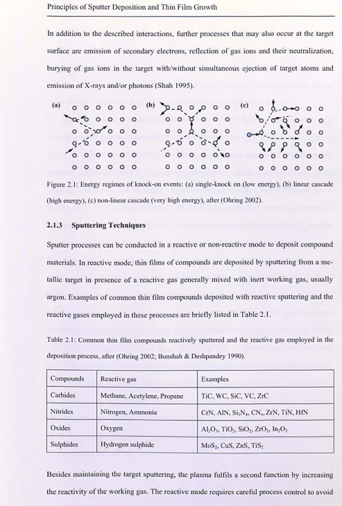
In certain energy ranges, the ion bombardment of the target surface leads to the ejection of target atoms due to collisions involving a momentum exchange from incoming ions to the target The ejection of target particles (sputtering) requires a sequence of collisions to change the momentum vector direction towards the target surface. In low energy knock-on processes (single knock-on), a target atom located on the surface receives only a glancing blow and may transfer its energy to a neighbouring surface atom that is then possibly ejected from the surface (Fig. 2.la). At higher energies, atoms undergo several collisions inside the target
before sputtering is initiated (Fig. 2.1 b). Instead of initiating a collision cascade, a primary knock-on atom can itself get reflected. In case when the impacting particle has a very high
energy, nearly all target atoms can be set in motion (Fig 2.lc), which leads to a non-linear collision cascade and, thus, nonlinear sputtering of atoms (Webb, Kerford & Way 1999).
Principles of Sputter Deposition and Thin Film Growth
In addition to the described interactions, further processes that may also occur at the target
surface are emission of secondary electrons, reflection of gas ions and their neutralization,
burying of gas ions in the target with/without simultaneous ejection of target atoms and
emission of X-rays and/or photons (Shah 1995).
(a) 0 0 0 0 0 0 (b)
)-l?
o'p 0 0 (c) 0
t _
_
o-o 0 0~"'o
'
,;'U/o-~
.
00 0 0 0
o
0
X
0 0 0 0 0,
0
'o'..if
0 0 0 0 0 0 0 00-6,,0
b
c!
0 0"
"o
''o,r/
,;
"
---.
0" .... 0 0 0 0 0 O .... t:> 0
~l
f
'\
0 0.- ....
"'0 "
,
0 0 0 0 0 0 0 0 0 0 , 0 0 0 0 0 0 0
0 0 0 0 0 0 0 0 0 0 0 0 0 0 0 0 0 0
Figure 2.1: Energy regimes of knock-on events: (a) single-knock on (low energy), (b) linear cascade
(high energy), (c) non-linear cascade (very high energy), after (Ohring 2002).
2.1.3 Sputtering Techniques
Sputter processes can be conducted in a reactive or non-reactive mode to deposit compound
materials. In reactive mode, thin films of compounds are deposited by sputtering from a m
e-tallic target in presence of a reactive gas generally mixed with inert working gas, usually
argon. Examples of common thin film compounds deposited with reactive sputtering and the
reactive gases employed in these processes are briefly listed in Table 2.1.
Table 2.1: Common tbin film compounds reactively sputtered and the reactive gas employed in the
deposition process, after (Obring 2002; Bunshah & Deshpandey 1990).
Compounds Reactive gas Examples
Carbides Methane, Acetylene, Propane TiC, WC, SiC, YC, zrC
itrides itrogen, Ammonia CrN, AIN, Si)N4, CN.,Zr , Ti ,HfN
Oxides Oxygen AhO), Ti02, Si02, Zr02, In2O)
Sulphides Hydrogen sulphide MoS2, eus, ZnS, TiS2
Besides maintaining the target sputtering, the plasma fulfils a second function by increasing
[image:46.509.4.497.22.752.2]