Abstract—In recent years, the semiconductor industry has been a high-growth business. Yield improvement becomes more and more important for semiconductor manufacturing process and it’s the important element to ensure the profitability. Defect spatial patterns impede yield and it reveal the root causes of the occurred defects. This research developed a defect spatial pattern recognition methodology. In this research, defect spatial patterns are classified into seven categories, Curve Type, Line Type, Local Type, Ring Type, Radial Type, and Repeat Type and Die Edge Type. Original defects are filtered to eliminate random defects. With random defect removed, a clustering method is designed to cluster systematic defects. Clustered defects are then analyzed with minimum rectangle. A feature extraction procedure based on wavelet transform is developed to extract features that represent different defect patterns. By setting feature vectors into feature space and applying hierarchical agglomerative algorithm to clustering, it is expected to reach the goal of description and classification. The presented methodology is verified with real industrial data from a famous semiconductor company. The experimental results show the presented methodology is able to recognize defect patterns with recognition accuracy of 95%.
Index Terms— Semiconductor, defect pattern,, feature extraction, wavelet transforms.
I. INTRODUCTION
Semiconductor manufacturing has become as one of important world industries. As a result of technology and information advancement, the integrated circuit (IC) chips are becoming more and smaller and its functions are more than before. The IC is the main components of electronic products and human being depends on it to be steadily on the increase. Therefore, the semiconductor manufacturing
Dr. S. F. Liu is with Department of Information Management, Yuanpei University of Technology, Hsichu County, 300, Taiwan(R.O.C) (phone: 886-3-538-1183; fax: 886-3-538-5353; e-mail: [email protected] ).
Dr. F. L. Chen is with Department of Industrial Engineering and Engineering Management, National Tsing Hua University, Hsichu County, 300, Taiwan(R.O.C) (phone: 886-3-571-7654; fax: 886-3-572-2685; e-mail: [email protected]).
Y. Y. Shi is with Department of Industrial Engineering and Engineering Management, National Tsing Hua University, Hsichu County, 300, Taiwan(R.O.C) (phone: 886-3-571-7654; fax: 886-3-572-2685; e-mail: [email protected] ).
S. M. Yu is with Department of Industrial Engineering and Engineering Management, National Tsing Hua University, Hsichu County, 300, Taiwan(R.O.C) (phone: 886-3-571-7654; fax: 886-3-572-2685; e-mail: [email protected] ).
C. S. Chang is with Department of Industrial Engineering and Engineering Management, National Tsing Hua University, Hsichu County, 300, Taiwan(R.O.C) (phone: 886-3-571-7654; fax: 886-3-572-2685; e-mail: [email protected] ).
industries expect more and more advancement.
However, yield improvement is the issue that always been discussed and is also the important element to ensure the profitability in semiconductor industry. The procedure of semiconductor manufacturing has become more and more sophisticated. There are over 300 steps in the semiconductor manufacturing processes. The collected data among these process steps are thus becoming high-dimensional and huge. Therefore, it is hard to discover root cause of low-yield situations. In order to meet the expectation on a high yield target, quick identification of the root cause becomes a vital issue.
The existence of defects on the wafer brings IC yield loss. Defects can be classified into random defects and systematic defects [1]. Random defects are scattered randomly on the wafer surface. Systematic defects are concentrated in a particular area of the wafer or defects that appear repetitively within a specific region. Systematic defects are usually induced by parametric problems that are associated with product design or wafer-processing accuracy [2]. Analysis of defects that are zonal provides clues to identify the equipment or process abnormality.
In practice, engineers usually spend much time checking the entire defect maps and choose the maps having spatial defect patterns. The engineers then use these results to adjust the process parameters to eliminate these defects or to perform further experiments to find out the source of the defects. Because the patterns are not well defined, the similarities between these patterns are difficult to determine. The process of defect classification is time-consuming, monotonous and costly and causes fatigue and eyestrain that in turn cause errors in classifications. In view of above-mentioned reasons, the objective of this research is to develop a defect spatial pattern recognition methodology to accurately recognize defect spatial patterns and assist engineers to quickly track process variations.
Prior researches had proposed their approaches to deal with defect classification. Kaempf uses statistic analysis method to classify defect into two types [3]. Chen and Liu use neural-network architecture named adaptive resonance theory network 1 (ART1) to classify defect into three types
[4]. However, their works limited to the types of defect patterns to be recognized and were unable to represent defect patterns with feature spaces. This research presented a defect map recognition methodology that covers much more defect patterns and increase recognition accuracy with wavelet transforms approach. In Section II, the problem of this paper is briefly described. The methodology we presented is illustrated in Section III while experiments results are given in Section IV. Section V is some conclusions of the experimental results.
Wavelet Transform Based Wafer Defect Map Pattern
Recognition System in Semiconductor Manufacturing
II. THE DEFINITION OF PROBLEM
In semiconductor manufacturing processes, the main cause of low yield is defect on the wafer. The defect distribution on the wafer depends on different factors including environmental changes, parametric control, condition of machines and human error. The engineers are able to track the root causes through defect analysis. In this research, we developed a defect map recognition methodology to classify seven defect patterns as shown in Table I. These defect pattern types are Line type, Curve type, Ring type, Local type, Radial type, Repeat type and Die Edge.
TABLE I
THE PATTERN-RELATED DEFECTS CATEGORIS
III. METHODOLOGY
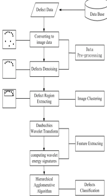
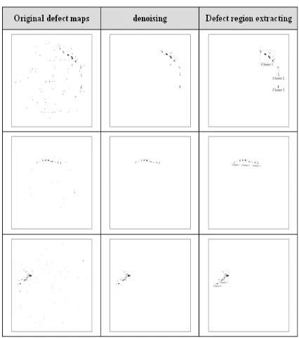
This section describes the architecture of the presented methodology. The first step is to transform the defect coordinates data into image format. Each black pixel in the image corresponds to a defect on the wafer. In order to achieve the high accuracy of pattern recognition, noise elimination procedure is necessary to remove the isolated defects and thus enhances the quality of defect maps in image format. Clustering algorithm is developed to subdivide defect map images into several regions. This research applies CURE for the clustering. In order to extract more precise features on defect map images, minimum rectangle is used to cover each clustered defects. Once all
[image:2.612.333.522.124.469.2]algorithm to group feature vectors into seven clusters. For each observation in the vector space will be assigned one cluster index. Each cluster will represent a defect pattern. Fig. 1 illustrates the entire architecture of the proposed methodology. Details for each steps are given below.
Fig. 1. The architecture of the proposed methodology
A. Defects Denoising
This research uses mask processing for noises reduction. Mask processing is denoted by the expression
( )
[
f
x
y
]
T
y
x
g
(
,
)
=
,
(1)where
f
( )
x
,
y
is the input image,g
( )
x
,
y
is the processed image, andT
is an operator onf
, defined over some neighborhood of( )
x
,
y
. In this research,( )
x
y
g
,
is given byN N
z
w
coefficient are one), and
z
ij is assigned a value of 1 if the defect falls in the location( )
i
,
j
, and otherwise it is assigned a value of 0. This research usesg
( )
x
,
y
to determine whether the defect located in( )
x
,
y
is a random defect or not [2].This research uses two masks to check whether the defect is a random defect or not. After determining the thresholds of two masks, big and small, the next step is to sweep the entire image pixel by pixel. The big max mask used to check large areas and mainly aimed at screen out the isolated defects. If there were not enough defects in a bigger mask, defects would be considered as random defects and are stripped off. However, parts of random defects still exit due to dense defects close to them. Therefore, the small mask is used to remove the defects that do not have enough neighbor defects.
B. Defect Region Extraction
After removing the isolated defects, the next step is defect region extracting by subdividing images into several regions. Each region will be covered by minimum rectangles. In comparison with other clustering methods, this research would use CURE method. CURE utilizes multiple representative points to evaluate the distance between clusters, thereby adjusting well to arbitrary shaped clusters and avoiding the single-link effect. Furthermore, the representative points provide information about the shape of clusters to facilitate the further analysis.
Guha and colleagues [5] stated that the input parameters of CURE algorithm are the input data set
S
containingn
points ind
-dimensional space and the desired number of clustersk
. Starting with the individual points as individual clusters, the closest pair of clusters is merged at each step to form a new cluster. The process is repeated until there are onlyk
remaining clusters. This research modifies the stopping condition to be that the process is repeated until the smallest distance of the closest pair of clusters among all clusters is greater than the pre-determined threshold. After CURE algorithm, use rectangular area of variable size of coordinates(
X
min,
X
max,
Y
min,
Y
max)
to cover each clustering defect. Table II illustrates the results of test samples after noise elimination and defect region extracting.TABLE II
THE RESULTS OF TEST SAMPLES AFTER DENOISING AND DEFECT REGION EXTRACTING
C. Feature Extraction
Feature extraction can reduce the dimensionality of pattern representation and help engineers to decide the defect patterns. This research adopts wavelet transformation to extract features.
Wavelet transformation has a characteristic of multi-resolution that makes features of the image more obvious. Each transformation can decompose original image into four sub-images, a low frequency sub-image and three high frequency sub images. Daubechies wavelet function is selected for the transformation.In order to decompose an image, a scaling function
ϕ
(
x
,
y
)
=
ϕ
(
x
)
ϕ
(
y
)
is introduced and the three two-dimensional wavelets are defined as the wavelet function of horizontal asψ
H(
x
,
y
)
=
ψ
(
x
)
ϕ
(
y
)
, the wavelet function of vertical asψ
V(
x
,
y
)
=
ϕ
(
x
)
ψ
(
y
)
, and the wavelet function of diagonal asψ
D(
x
,
y
)
=
ψ
(
x
)
ψ
(
y
)
[6]. This decomposition provides sub-images corresponding to different resolution levels and orientations. After two-level wavelet transformation wavelet energy signatures of each sub-image is calculated as equation (3).∑
=
=
Nk k
i
C
N
E
1 2 2
1
(3)
D. Pattern Classification
[image:4.612.326.539.121.361.2]A set of features are extracted from previous step, and these features are commonly called feature vectors that constitutes a representation of the data. The features vectors constitute the feature vector space are shown in Fig. 2.
Fig. 2. The feature vector space
IV. EXPERIMENTAL RESULT
Recognition accuracy is an important factor to measure the ability of system. The experimental results are summarized in Table III there are 65 defect pattern samples tested in this experiment. The average accuracy of recognition is 95%.
TABLE III
THE EXPERIMENTAL RESULTS
Defect pattern Sample
quantity Accuracy
Curve 5 60%
Line 9 100%
Ring 12 100%
Local 12 92%
Radial 7 100%
Repeat 11 100%
Die edge 9 100%
Total 65 95%
Note that the presented system failed to recognize two curve types and one local type. These 3 samples are depicted
line type or curve type. The system failed to recognize local type is due to the large region of clustering defects and small density.
TABLE IV
FAILED TO RECOGNITION DEFECT PATTERNS
Usually statis1tical methods and neural-network approaches are applied to recognize defect patterns. Table V illustrates the comparisons between presented methodology, statistical and neural network approaches.
V. CONCLUSIONS
TABLE V METHOLOGY COMPARSONS
Methods
Items Statistical Neural network
Proposed methodology Inspection
areas
Whole die area
Whole die area
Clustering defect
Limitation
1.Need the hypothesis of
distributions 2.Hard to deal with complex defect patterns
1.Need lead-time to construct the
entire network 2.Hard to decide the parameter
1.Incapable of dealing
with the defects with a discontinuous distribution
Detectabl e defect patterns
Scratch type Zone type
Scratch type Zone type Ring type
Curve type Line type Local type
Ring type Radial type Repeat type Die Edge
type
Accuracy Medium High High
REFERENCES
[1] Mirza, A. I. , Donoghue, G., O’ ,Drake, A. W.,”Spatial Yield Modeling for Semiconductor Wafers” , IEEE/SEMI Advanced Semiconductor Manufacturing Conference, 1995, pp.276-281. [2] Friedman, D. J., Hansen, M. H., Nair, V. N., and James, D. A.,
“Model-free estimation of defect clustering in integrated circuit fabrication” IEEE Transactions on Semiconductor Manufacturing, 1997, pp.344-359.
[3] Kaempf, U., “The Binomial Test: A Simple Tool to Identify Process Problems,” IEEE Transactions on Semiconductor Manufacturing, 1995, pp.160-165.
[4] Chen, F. L., Liu, S. F., “A Neural-Network Approach To Recognize Defect Spatial Pattern In Semiconductor Fabrication” IEEE TRANSACTIONS ON SEMICONDUCTOR MANUFACTURING, VOL.13, NO.3, 2000, pp.366-373.
[5] Guha, Sudipto, Rastogi, Rajeev, and Shim, Kyuseok, “CURE: An Efficient Clustering Algorithm for Large Databases,” ACM-SIGMOD International Conference on Management of Data, 2001, pp.73-84. [6] Gonzalez, R. C., Woods, R. E., Rafael C. G., and Richard, E.W.,