in Large Area Electronics: A Review
OJO, Ayotunde Adigun and DHARMADASA, I
<http://orcid.org/0000-0001-7988-669X>
Available from Sheffield Hallam University Research Archive (SHURA) at:
http://shura.shu.ac.uk/22159/
This document is the author deposited version. You are advised to consult the
publisher's version if you wish to cite from it.
Published version
OJO, Ayotunde Adigun and DHARMADASA, I (2018). Electroplating of
semiconductor Materials for Applications in Large Area Electronics: A Review.
Coatings, 8 (8), p. 262.
Copyright and re-use policy
See
http://shura.shu.ac.uk/information.html
coatings
Review
Electroplating of Semiconductor Materials for
Applications in Large Area Electronics: A Review
Ayotunde Adigun Ojo * and Imyhamy Mudiy Dharmadasa
Electronic Materials and Sensors Group, Materials and Engineering Research Institute, Sheffield Hallam University, Sheffield S1 1WB, UK; [email protected]
* Correspondence: [email protected]; Tel.: +44-114-225-6910; Fax: +44-114-225-6930
Received: 26 June 2018; Accepted: 25 July 2018; Published: 27 July 2018
Abstract: The attributes of electroplating as a low-cost, simple, scalable, and manufacturable
semiconductor deposition technique for the fabrication of large-area and nanotechnology-based device applications are discussed. These strengths of electrodeposition are buttressed experimentally using techniques such as X-ray diffraction, ultraviolet-visible spectroscopy, scanning electron microscopy, atomic force microscopy, energy-dispersive X-ray spectroscopy, and photoelectrochemical cell studies. Based on the results of structural, morphological, compositional, optical, and electronic properties evaluated, it is evident that electroplating possesses the capabilities of producing high-quality semiconductors usable for producing excellent devices. In this paper we will describe the progress of electroplating techniques mainly for the deposition of semiconductor thin film materials and their treatment processes, and fabrication of solar cells.
Keywords:electroplating; semiconductors; large-area electronics; characterisation; solar cells
1. Introduction
Electroplating has been well explored over the years especially for the purification, extraction, protection, and coating of semiconductors, metals, and metalloids in the industrial sector [1] to achieve diverse characteristic properties. The use of the electroplating technique in the deposition of semiconductor materials dates back to the 1970s [2–4], with the deposition of semiconductors from the II-VI group. The ascendance of the electrodeposition of semiconductor material led to the growth and fabrication of CdS/CdTe-based solar cell devices within a decade afterwards [5]. The fabrication of thin-film solar cells with photovoltaic conversion efficiency of ~10% was the stimulus for an intense global research into electrodeposited semiconductor compounds. The research also spanned into the electrodeposition of II-VI semiconductor materials such as ZnTe [6], ZnSe [6], ZnS [7], ZnO [8], etc., and spread into semiconductor material compounds in the binary (III-V, IV-VI), ternary (CuInSe2) [9,10], and quaternary (Cu2ZnSnS4, CuInGaSe2) groups [11]. The electroplating of elemental semiconductors and other wide bandgap nitrides has also been captured in the literature. This communication critically appraises the strengths, weaknesses, potentials, and the state-of-the-art electroplating technique in the fabrication of large-area electronics and other macro-electronic devices such as photovoltaic (PV) solar panels and display devices.
2. An Overview of Electrodeposition Technique
Electrodeposition is the process of depositing elemental or compound metals or semiconductors on a conducting substrate by passing an electric current through an ionic electrolyte in which metal or semiconductor ions are present [12]. The passage of current is required due to the inability of the chemical reaction resulting in the deposition of the solid material on the conducting substrate to proceed on its own as a result of positive free energy change∆Gof the reaction.
Coatings2018,8, 262 2 of 17
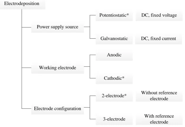
Electrodeposition can be categorised based on power supply source, working electrode, and electrode configuration (as shown in Figure1), but the basic deposition mechanism and setup remains similar. The basic deposition mechanism entails the flow of electrons from the power supply to the cathode. The positively charged cations are attracted towards the cathode and negatively charged anions to the anode. The cations or anions are neutralised electrically by gaining electrons (through reduction process) or losing electrons (through oxidation process) and being deposited on the working electrode (WE), respectively [12].
2. An Overview of Electrodeposition Technique
Electrodeposition is the process of depositing elemental or compound metals or semiconductors on a conducting substrate by passing an electric current through an ionic electrolyte in which metal or semiconductor ions are present [12]. The passage of current is required due to the inability of the chemical reaction resulting in the deposition of the solid material on the conducting substrate to
proceed on its own as a result of positive free energy change ∆G of the reaction.
[image:3.595.144.458.201.416.2]Electrodeposition can be categorised based on power supply source, working electrode, and electrode configuration (as shown in Figure 1), but the basic deposition mechanism and setup remains similar. The basic deposition mechanism entails the flow of electrons from the power supply to the cathode. The positively charged cations are attracted towards the cathode and negatively charged anions to the anode. The cations or anions are neutralised electrically by gaining electrons (through reduction process) or losing electrons (through oxidation process) and being deposited on the working electrode (WE), respectively [12].
Figure 1. The main categories of electrodeposition technique.
The typical electrodeposition (ED) setup of a two-electrode (2E) configuration, as shown in Figure 2a, consists of a deposition container (beaker), deposition electrolyte, magnetic stirrer, hotplate, power supply, a working electrode, a counter electrode, and an optional reference electrode (RE) in the case of a three-electrode (3E) configuration (see Figure 2b). The use of a potentiostatic power source was due to the effect of deposition voltage on the atomic percentage composition of elements in the electrodeposited layer, which is one of the factors determining the conductivity type [13,14]. Cathodic deposition is mainly utilized due to its ability to produce stoichiometric thin-films with good adherence to the substrate as compared to anodic deposition [15]. Conversely, the galvanostatic electrodeposition is controlled and measured by maintaining constant current density through an electrolytic cell disregarding the changes in the resistance due to the deposited electroplated layer.
The 2E configuration, as shown in Figure 2a, was utilised due to its industrial applicability,
process simplification, and also to eliminate possible Ag+- and K+-ion doping [16,17], which may
emerge from the Ag/AgCl or saturated calomel electrode (SCE) reference electrodes (see Figure 2b).
Taking the electrodeposition of n-CdS and n-CdTe layers which are respectively utilised as the main
window and absorber layers in this work into perspective, both K+ and Ag+ from group I of the
periodic table are considered as p-type dopants. Therefore, any leakage of K+ and Ag+ into the
electrolytic bath may result in compensation leading to the growth of highly resistive material which has a detrimental effect on the efficiency of fabricated solar cells. This has been experimentally shown and reported in the literature [16].
Electrodeposition
Power supply source
Working electrode Potentiostatic* Galvanostatic Anodic Cathodic* Electrode configuration 2-electrode*
3-electrode With reference electrode Without reference
electrode DC, fixed current DC, fixed voltage
Figure 1.The main categories of electrodeposition technique.
The typical electrodeposition (ED) setup of a two-electrode (2E) configuration, as shown in Figure2a, consists of a deposition container (beaker), deposition electrolyte, magnetic stirrer, hotplate, power supply, a working electrode, a counter electrode, and an optional reference electrode (RE) in the case of a three-electrode (3E) configuration (see Figure2b). The use of a potentiostatic power source was due to the effect of deposition voltage on the atomic percentage composition of elements in the electrodeposited layer, which is one of the factors determining the conductivity type [13,14]. Cathodic deposition is mainly utilized due to its ability to produce stoichiometric thin-films with good adherence to the substrate as compared to anodic deposition [15]. Conversely, the galvanostatic electrodeposition is controlled and measured by maintaining constant current density through an electrolytic cell disregarding the changes in the resistance due to the deposited electroplated layer.Coatings 2018, 8, x FOR PEER REVIEW 3 of 17
Figure 2. Typical (a) two-electrode and (b) three-electrode electrodeposition setups.
The two-electrode electrodeposition configurations are not without challenges, with the main challenge being the fluctuation or drop in the potential measured across the cathode and the anode during deposition. This is due to the alteration in resistivity of the substrate with increasing semiconductor layer thickness and the change in the ionic concentration of the electrolyte. For the three-electrode configuration, the potential difference is measured across the working and the reference electrodes, while the measured current is between the working and the counter electrodes. In general, other factors such as the pH of the electrolyte [18], applied deposition potential [13,14], deposition temperature [19], stirring rate [20], deposition current density, duration of deposition and thickness [21], underlying substrate [22], and concentration of ions in the deposition electrolyte [18] affects the electrodeposition process and the properties of the deposited layers. Recent publications have demonstrated the similarities between electrodeposited semiconductors using three-electrode and two-electrode electroplating configurations [23,24]. The electrodeposition of both elements and
compounds is governed by Faraday’s laws of electrodeposition as mathematically depicted in
Equation (1).
1
ρ
ρ
itM
JtM
T
nF
A
nF
=
=
(1)where T is the thickness (cm), J is current density (A cm−2), t is the deposition time (s), M is the
molecular mass (g mol−1), n is the number of electrons transferred in the chemical reaction for the
formation of 1 mole of substance in g cm−3, F is Faraday’s constant (96,485 C mol−1), and ρ is the density
(g cm−3). It should be noted that Faraday’s law of electrolysis assumes that all electronic charges
passing through the electrolyte contribute to the deposition of deposited material layer without any consideration of the resistance losses in the system and electronic charge contribution to the decomposition of solvent into its constituent ions [25].
3. Factors Influencing Electrodeposition
3.1. Solutes, Solvents, and Deposition Electrolytes
The effects of the incorporated solute and solvent utilised are of importance in electrodeposition.
Taking the electrodeposition of CdS into consideration, sodium-(Na)-based precursor (Na2S2O3) has
been often utilised [26,27]. Although sodium (Na) ions are not electrodeposited at low cathodic voltages, the incorporation of Na in CdS films is achievable through adsorption, absorption or chemical reactions as a result of increased Na accumulation in the electrolytic bath. It should be noted that Na is a p-type dopant in CdS [28] resulting in increasing electrical resistivity of subsequent CdS
layers due to Na accumulation. Further to this, the Na-based precursor (Na2S2O3) is also associated
with the precipitation of sulphur during the electroplating. Recent understanding has shown that the
replacement of the well-established sulphur precursor with thiourea (NH2CSNH2) (which is more
associated with chemical bath deposition (CBD) technique) results in the reduction/elimination of sulphur precipitate [29,30].
- +
Anode (high purity carbon rod) Beaker Electroplated layer Electrolyte Magnetic stirrer Glass/FTO (Conducting substrate) Cathode (high purity carbon rod)
Electric hot plate
A Ammeter (a)
- +
Anode (high purity carbon rod) Beaker Electroplated layer Electrolyte Magnetic stirrer Glass/FTO (Conducting substrate) Cathode (high purity carbon rod)
Electric hot plate
Reference electrode (Ag/AgCl, SCE etc.) A
V Ammeter
Voltmeter
(b)
- +
Anode (high purity carbon rod) Beaker Electroplated layer Electrolyte Magnetic stirrer Glass/FTO (Conducting substrate) Cathode (high purity carbon rod)
Electric hot plate
A Ammeter (a)
- +
Anode (high purity carbon rod) Beaker Electroplated layer Electrolyte Magnetic stirrer Glass/FTO (Conducting substrate) Cathode (high purity carbon rod)
Electric hot plate
Reference electrode (Ag/AgCl, SCE etc.) A
V Ammeter
Voltmeter
(b)
Coatings2018,8, 262 3 of 17
The 2E configuration, as shown in Figure2a, was utilised due to its industrial applicability, process simplification, and also to eliminate possible Ag+- and K+-ion doping [16,17], which may emerge from the Ag/AgCl or saturated calomel electrode (SCE) reference electrodes (see Figure2b). Taking the electrodeposition of n-CdS and n-CdTe layers which are respectively utilised as the main window and absorber layers in this work into perspective, both K+and Ag+ from group I of the periodic table are considered as p-type dopants. Therefore, any leakage of K+ and Ag+ into the electrolytic bath may result in compensation leading to the growth of highly resistive material which has a detrimental effect on the efficiency of fabricated solar cells. This has been experimentally shown and reported in the literature [16].
The two-electrode electrodeposition configurations are not without challenges, with the main challenge being the fluctuation or drop in the potential measured across the cathode and the anode during deposition. This is due to the alteration in resistivity of the substrate with increasing semiconductor layer thickness and the change in the ionic concentration of the electrolyte. For the three-electrode configuration, the potential difference is measured across the working and the reference electrodes, while the measured current is between the working and the counter electrodes. In general, other factors such as the pH of the electrolyte [18], applied deposition potential [13,14], deposition temperature [19], stirring rate [20], deposition current density, duration of deposition and thickness [21], underlying substrate [22], and concentration of ions in the deposition electrolyte [18] affects the electrodeposition process and the properties of the deposited layers. Recent publications have demonstrated the similarities between electrodeposited semiconductors using three-electrode and two-electrode electroplating configurations [23,24]. The electrodeposition of both elements and compounds is governed by Faraday’s laws of electrodeposition as mathematically depicted in Equation (1).
T=
1 nF
itM
$A
=
JtM nF$
(1)
whereT is the thickness (cm),Jis current density (A cm−2),tis the deposition time (s), Mis the molecular mass (g mol−1),nis the number of electrons transferred in the chemical reaction for the formation of 1 mole of substance in g cm−3,Fis Faraday’s constant (96,485 C mol−1), and$is the
density (g cm−3). It should be noted that Faraday’s law of electrolysis assumes that all electronic charges passing through the electrolyte contribute to the deposition of deposited material layer without any consideration of the resistance losses in the system and electronic charge contribution to the decomposition of solvent into its constituent ions [25].
3. Factors Influencing Electrodeposition
3.1. Solutes, Solvents, and Deposition Electrolytes
The effects of the incorporated solute and solvent utilised are of importance in electrodeposition. Taking the electrodeposition of CdS into consideration, sodium-(Na)-based precursor (Na2S2O3) has been often utilised [26,27]. Although sodium (Na) ions are not electrodeposited at low cathodic voltages, the incorporation of Na in CdS films is achievable through adsorption, absorption or chemical reactions as a result of increased Na accumulation in the electrolytic bath. It should be noted that Na is a p-type dopant in CdS [28] resulting in increasing electrical resistivity of subsequent CdS layers due to Na accumulation. Further to this, the Na-based precursor (Na2S2O3) is also associated with the precipitation of sulphur during the electroplating. Recent understanding has shown that the replacement of the well-established sulphur precursor with thiourea (NH2CSNH2) (which is more associated with chemical bath deposition (CBD) technique) results in the reduction/elimination of sulphur precipitate [29,30].
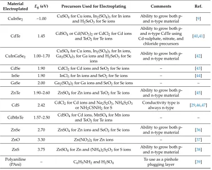
CdI−3, and CdI24− are formed in aqueous solution [32,33] debarring the deposition of Cd and the co-deposition of CdTe. It is noteworthy that CdTe from other Cd precursors have been explored and reported in the literature [34,35]. Therefore, the choice of solute and solvent for electroplating purposes is a factor to reckon with in addition to a number of other factors inherent in the electrodeposition process to achieve superior qualities of electroplated semiconductor materials. This understanding has been accrued for over two decades of exploration, and careful examination of grown semiconductors at Solar Energy Group within Sheffield Hallam University (SHU), in addition to the literature. A large number of semiconductors explored in SHU and documented in the literature [9,29,36–47] is summarised in Table1.
Table 1. Summary of explored electronic materials to date at authors’ research group using electroplating from aqueous solutions.
Material
Electroplated Eg(eV) Precursors Used for Electroplating Comments Ref.
CuInSe2 ~1.00 CuSO4for Cu ions, Inand H 2(SO4)3for In ions 2SeO3for Se ions
Ability to grow both
p-and n-type material [9]
CdTe 1.45 CdSO4or Cd(NO3)2or CdCl2for Cd ions and TeO2for Te ions
Ability to grow both p-and n-type CdTe using Cd-sulphate, nitrate, and
chloride precursors
[40,41]
CuInGaSe2 1.00–1.70
CuSO4for Cu ions, In2(SO4)3for In ions, Ga2(SO4)3for Ga ions and H2SeO3for Se
ions
Ability to grow both
p-and n-type material [42]
CdSe 1.90 CdCl2for Cd ions and SeO2for Se ions – [43]
InSe 1.90 InCl3for In ions and SeO2for Se ions – [44]
GaSe 2.00 Ga2(SO4)2for Ga ions and SeO2for Se ions – –
ZnTe 1.90–2.60 ZnSO4for Zn ions and TeO2for Te ions Ability to grow both p-and n-type material [45]
CdS 2.42 CdCl2for Cd ions and Na2S2O3, NH4S2O3 or NH2CSNH2for S
Conductivity type is
always n-type [29,46,47]
CdMnTe 1.57–2.50 CdSO4for Cd ions, MnSO4for Mn ions
and TeO2for Te ions – –
ZnSe 2.70 ZnSO4for Zn ions and SeO2for Se ions Ability to grow both p-and n-type material [36]
ZnO 3.30 Zn(NO3)2for Zn ions – [37]
ZnS 3.75 ZnSO4for Zn and (NH4)2S2O3for S ions Ability to grow both p-and n-type material [38]
Polyaniline
(PAni) – C6H5NH2and H2SO4
To use as a pinhole
plugging layer [39]
3.2. Electrolytic Bath pH Value
Coatings2018,8, 262 5 of 17
and increase in the deposition current density [54]. Furthermore, the effect of pH on the dissociation of common solvent such as water is also well documented in the literature [55], with the notion that an increase in the acidity of an electroplating bath results in the increase in the concentration of dissociated ions in the aqueous solution [55]. Due to the increased ionic concentration, the deposition current density increases until it stabilises or continues to increase, depending on the composition of the solution.
3.3. Deposition Temperature
It is a known fact that an increase in the temperature of a matter increases the motion of the molecules inside it. As such, the electrolytic bath temperature increases solubility of the solvent, catalyses the reactions, energizes the ions, and increases the transport number, which results in an increase in the deposition current density and rate of deposition of constituent elements or compounds. Further to this, the work performed on electrodeposition depicted that an increase in the crystallinity of as-deposited semiconductor material is achievable at higher growth temperature [3,56]. For electroplated semiconductor materials from aqueous solution, there is a limitation on the growth temperature due to the boiling temperature of water at 100◦C under standard atmospheric pressure, while the electroplating from other electrolytic baths can go as high as 160◦C [31]. Deposition of materials at higher temperature provides energy required for ions/atoms to move around and deposit in a regular crystalline pattern.
3.4. Deposition Current Density
With regards to Faraday’s law of electrodeposition, the deposition current density is directly related to the thickness of the deposited layer. Thus, the deposition current density is dependent on factors effecting the energizing of the inherent ions in the electrolyte such as stirring rate, bath temperature, concentration of constituent [57], and electrical conductivity of the substrate amongst other constraints. While a gradual alteration in the deposition current density is expected depending on the electrical conductivity of the electroplated layers.
With respect to semiconductor materials such as CdTe, the literature depicts the effect of current density on the morphological, compositional and the structural properties of the deposited layer [58,59]. Based on the deposition configuration, it can be inferred that the deposition current density of three-electrode configuration and two-electrode deposition configuration vary. CdTe with optimal characteristic properties deposited from a three-electrode deposition is known to lie between ~(0.3–0.6) mA cm−2 [57,60]. While two-electrode electrodeposition has been documented to produce CdTe layers with an optimal characteristic property of ~(0.15–0.18) mA cm−2[61]. Under potentiostatic mode, Basol (1988) clarified that the deposition current density for CdTe electroplating depends on the tellurium concentration in the electrolyte [57]. The incorporation of excessive Te can alter the composition of the deposited CdTe, conduction type top-CdTe due to Te-richness [62], and reduce adhesion on the underlying substrate. Reduction in the adhesion of CdTe may also occur due to the deficiency of Te concentration in the electrolytic bath. In either condition (excess or deficiency of Te concentration in the electrolyte), the crystallinity, morphology, and adhesion of the ensued CdTe layer suffer. In addition, current density during co-deposition of competing ions such as Ga3+and Fe2+in the electroplating of Fe–Ga alloys is a determinant of the Fe:Ga elemental composition ratio of the resultant alloy [63].
3.5. Duration of Deposition and Thickness
the highest electric field is experienced at the peaks of the rough surfaces. The nucleation of the electroplated material spreads out through to the lowest valley from the initiation rough surface peaks resulting into columnar nature of the deposited layers [14]. The potency of this mechanism is highly influential at the initial stages of deposition due to unevenness of the deposited layer thickness characterised by pin-holes, voids, gaps, and high dislocation density within the semiconductor material [21]. This characteristic property is detrimental when a thin semiconductor layer with a thickness of <100 nm is required [21].
4. Strengths and Weaknesses of Electrodeposition
4.1. Strengths of Electrodeposition
4.1.1. Electrolytic Bath Life Longevity and Self -Purification
At the start of an electrolytic bath, electro-purification of the bath is highly essential to reduce and eliminate the impurity level, which is mostly incorporated in the precursors amongst other impurity sources. It should be noted that even with a high purity precursor with 99.999% purity, it can carry an impurity level of 10 ppm. Purification is essential due to the effect of impurities even in ppm levels [65] on the characteristic properties of electroplated semiconductor materials. It should be noted that electro-purification of a bath must be performed using similar deposition parameters (such as bath temperature, pH, stirring rate, etc.) to the semiconductor deposition. The electro-purification potential utilised should be lower than the deposition potential range of the required elements established using cyclic voltammetry. Based on this characteristic property of electroplating technique, the more layers deposited, the purer the electrolyte and the electroplated semiconductor gets due to the gradual reduction of background impurities and improved material property. This property not only increases the purity of the electrolyte and the deposited semiconductor, but also increases the longevity of the bath as compared to the batch process of chemical bath deposition (CBD) technique.
To further mitigate other sources of impurities, a fraction of researchers choose two-electrode over the three-electrode configuration to avoid possible impurities from the reference electrode. While the usage of Teflon-ware (polypropylene beaker) is necessitated to house the electrolyte due to possible leaching of elemental sodium and other dopants from glass-wares [66] into acidic electrolytes.
4.1.2. Ease of Doping Intrinsic and Extrinsic
Coatings2018,8, 262 7 of 17
[image:8.595.125.470.87.272.2]Coatings 2018, 8, x FOR PEER REVIEW 7 of 17
Figure 3. Photoelectrochemical (PEC) cell measurement signal for (a) CuInSe2 and (b) CuInGaSe2 with
increasing cathodic voltages. Note the ability to grow p+, p, i, n, and n+ materials from the same
electrolyte, simply by varying the deposition voltage. Reproduced from [68,70] with permission; Copyright 2004 Sheffield Hallam University.
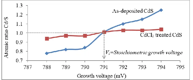
The effect of cathodic voltage on the elemental composition of binary semiconductors has also been demonstrated and documented in the literature [14,62]. The effect of alteration in the growth voltage on the elemental composition of electroplated materials even for as low as 1 mV step has been documented [29] (see Figure 4).
[image:8.595.134.464.418.556.2]The ease of intrinsic doping and the effect of extrinsic doping of electroplated semiconductor materials have been well established in the literature [65,71]. Due to the simplicity of ED, doping at the ppm level is made possible [65,71,72].
Figure 4. Atomic composition ratios of Cd to S in as-deposited and CdCl2 treated CdS thin films at
different deposition cathodic voltages.
4.1.3. Bandgap Engineering Capability
The control or alteration of the bandgap of materials (with emphasis on semiconductor) is easily achievable in electrodeposition techniques. Typically, this can be achieved by controlling the atomic composition of the elemental component of the semiconductor material. Intrinsically, electrodeposition has the ability to change the composition of growing material by a simple alteration of the cathodic
voltage [38,68–70]. An ensuing alteration in the bandgap of grown semiconductor material due to
change in the growth cathodic voltage has been documented in the literature [42]. It is well known
that an increase in the atomic concentration of Ga in CuInGaSe2 by increasing the cathodic voltage
increases the bandgap of CuInGaSe2. While a reduction in the cathodic voltage of the CuInGaSe2
results in the reduction of bandgap due to the richness of Cu [42] (see Figure 5). This ability provides
the ease of bandgap engineering of semiconductor material such as CuInGaSe2 between ~1.00 and
Figure 3. Photoelectrochemical (PEC) cell measurement signal for (a) CuInSe2 and (b) CuInGaSe2
with increasing cathodic voltages. Note the ability to grow p+, p, i, n, and n+ materials from the same electrolyte, simply by varying the deposition voltage. Reproduced from [68,70] with permission; Copyright 2004 Sheffield Hallam University.
The effect of cathodic voltage on the elemental composition of binary semiconductors has also been demonstrated and documented in the literature [14,62]. The effect of alteration in the growth voltage on the elemental composition of electroplated materials even for as low as 1 mV step has been documented [29] (see Figure4).
Coatings 2018, 8, x FOR PEER REVIEW 7 of 17
Figure 3. Photoelectrochemical (PEC) cell measurement signal for (a) CuInSe2 and (b) CuInGaSe2 with
increasing cathodic voltages. Note the ability to grow p+, p, i, n, and n+ materials from the same
electrolyte, simply by varying the deposition voltage. Reproduced from [68,70] with permission; Copyright 2004 Sheffield Hallam University.
The effect of cathodic voltage on the elemental composition of binary semiconductors has also been demonstrated and documented in the literature [14,62]. The effect of alteration in the growth voltage on the elemental composition of electroplated materials even for as low as 1 mV step has been documented [29] (see Figure 4).
The ease of intrinsic doping and the effect of extrinsic doping of electroplated semiconductor materials have been well established in the literature [65,71]. Due to the simplicity of ED, doping at the ppm level is made possible [65,71,72].
Figure 4. Atomic composition ratios of Cd to S in as-deposited and CdCl2 treated CdS thin films at
different deposition cathodic voltages.
4.1.3. Bandgap Engineering Capability
The control or alteration of the bandgap of materials (with emphasis on semiconductor) is easily achievable in electrodeposition techniques. Typically, this can be achieved by controlling the atomic composition of the elemental component of the semiconductor material. Intrinsically, electrodeposition has the ability to change the composition of growing material by a simple alteration of the cathodic
voltage [38,68–70]. An ensuing alteration in the bandgap of grown semiconductor material due to
change in the growth cathodic voltage has been documented in the literature [42]. It is well known
that an increase in the atomic concentration of Ga in CuInGaSe2 by increasing the cathodic voltage
increases the bandgap of CuInGaSe2. While a reduction in the cathodic voltage of the CuInGaSe2
results in the reduction of bandgap due to the richness of Cu [42] (see Figure 5). This ability provides
the ease of bandgap engineering of semiconductor material such as CuInGaSe2 between ~1.00 and
Figure 4.Atomic composition ratios of Cd to S in as-deposited and CdCl2treated CdS thin films at
different deposition cathodic voltages.
The ease of intrinsic doping and the effect of extrinsic doping of electroplated semiconductor materials have been well established in the literature [65,71]. Due to the simplicity of ED, doping at the ppm level is made possible [65,71,72].
4.1.3. Bandgap Engineering Capability
the bandgap of CuInGaSe2. While a reduction in the cathodic voltage of the CuInGaSe2results in the reduction of bandgap due to the richness of Cu [42] (see Figure5). This ability provides the ease of bandgap engineering of semiconductor material such as CuInGaSe2between ~1.00 and 2.20 eV. Extrinsically, this observation has also been documented for electroplated binary semiconductor materials such as CdTe doped with Ga [65] amongst others. The bandgap of the resulting doped semiconductor directly affected the incorporated dopant even at the parts per million level [65,71].
Coatings 2018, 8, x FOR PEER REVIEW 8 of 17
[image:9.595.156.442.183.346.2]2.20 eV. Extrinsically, this observation has also been documented for electroplated binary semiconductor materials such as CdTe doped with Ga [65] amongst others. The bandgap of the resulting doped semiconductor directly affected the incorporated dopant even at the parts per million level [65,71].
Figure 5. Energy bandgap variation for CuInGaSe2 as a function of the cathodic voltage.
4.1.4. Low Cost and Simplicity
There are over 14 different and well-established techniques to grow thin-film semiconductor materials [73] which can be broadly categorised under physical or chemical deposition. Physical deposition refers to the technologies in which material is released from a source and deposited on a substrate using thermodynamic, electromechanical or mechanical processes [1,74]. Chemical deposition techniques are accomplished by the utilisation of precursors either in their liquid or gaseous state to produce a chemical reaction on the surface of a substrate, leaving behind chemically deposited thin-film coatings on the substrate. Electrodeposition falls under chemical deposition techniques which can be carried out in an uncontrolled environment and without a vacuum system. The setup for electroplating which is mainly constituted of a computerized potentiostat and hotplate/magnetic stirrer with a cost implication of less than £5000 as compared to other techniques
such as the well-established metallorganic chemical vapour deposition (MOCVD) or close space
sublimation (CSS) system with a high initial cost implication of about £1 million for a laboratory setup. In addition, these systems have limitations as concerning the materials that can be grown. Furthermore, the relatively low heat energy required during growth and post-growth treatment makes electroplating a more energy-economic deposition technique as compared to a large number of other techniques. More importantly, grown semiconductor layers using cost-effective electroplating techniques are comparable to semiconductor layers grown using highly expensive techniques [29,75], and they all require post-deposition treatments [76,77].
4.1.5. Scalability and Manufacturability
The scalability and manufacturability of electroplating has been demonstrated on an industrial scale by British Petroleum (BP) Solar in the 1980s and 1990s [78,79]. BP Solar manufactured
CdTe-based solar cells with a solar panel area ~1 m2 with a conversion efficiency of ~10% [78,79]. As
compared to the laboratory scale setup as shown in Figure 2, scaling up requires a larger tank to contain the electrolyte and multi-plate cathode attached to multiple conducting substrates. The use of larger tanks and multi-plate cathode increases the throughput of deposited layers and an added advantage of electroplating on intricate shapes and designs.
1.0
1.4
1.8
2.2
0.2
0.4
0.6
0.8
1.0
1.2
1.4
1.6
B
na
dg
ap
(e
V
)
Cathodic potential (V)
Bandgap
variation
trendline
Figure 5.Energy bandgap variation for CuInGaSe2as a function of the cathodic voltage.
4.1.4. Low Cost and Simplicity
There are over 14 different and well-established techniques to grow thin-film semiconductor materials [73] which can be broadly categorised under physical or chemical deposition. Physical deposition refers to the technologies in which material is released from a source and deposited on a substrate using thermodynamic, electromechanical or mechanical processes [1,74]. Chemical deposition techniques are accomplished by the utilisation of precursors either in their liquid or gaseous state to produce a chemical reaction on the surface of a substrate, leaving behind chemically deposited thin-film coatings on the substrate. Electrodeposition falls under chemical deposition techniques which can be carried out in an uncontrolled environment and without a vacuum system. The setup for electroplating which is mainly constituted of a computerized potentiostat and hotplate/magnetic stirrer with a cost implication of less than £5000 as compared to other techniques such as the well-established metallorganic chemical vapour deposition (MOCVD) or close space sublimation (CSS) system with a high initial cost implication of about £1 million for a laboratory setup. In addition, these systems have limitations as concerning the materials that can be grown. Furthermore, the relatively low heat energy required during growth and post-growth treatment makes electroplating a more energy-economic deposition technique as compared to a large number of other techniques. More importantly, grown semiconductor layers using cost-effective electroplating techniques are comparable to semiconductor layers grown using highly expensive techniques [29,75], and they all require post-deposition treatments [76,77].
4.1.5. Scalability and Manufacturability
Coatings2018,8, 262 9 of 17
4.2. Weaknesses of Electrodeposition
One of the main disadvantages of electrodeposition includes comparatively low rates of deposition and the need for a conducting substrate as the working electrode in the electroplating setup. Due to this requirement, using conventional characterisation techniques such as the Hall effect to determine the electrical properties of the deposited layers on FTO, for example, will not be possible due to the underlying conducting layer.
4.2.1. Instability of Current Density during Deposition
The control of the electrodeposition process due to the alteration of current density with increasing deposition layer thickness is a challenge (under potentiostatic condition). The electroplating of materials with electrical conductivity levels lower than the primary substrate results in the reduction of current density with a direct relationship with the thickness of the deposited material [80]. This observation is common for both 2E and 3E electroplating configurations, but the applied voltage can vary slightly in 2E configuration.
4.2.2. Control and Regulation of Ions within the Electrolytic Bath
The chemical concentration of ionic species in an electrolytic bath is defined during bath creation, but the control, regulation and measurement of ionic concentration within the electrolytic bath during electroplating remains a challenge. This is as a result of the depletion in the ionic concentration and the inability to gauge/measure the concentration change during and after initial deposition, therefore replenishing the bath with the appropriate chemical concentration becomes difficult and thereby reducing reproducibility tendencies of electroplated layers.
4.2.3. Formation of Solution-Based Complexes
There is a possibility for the formation of complexes within the electrolyte which might be debarring the deposition of an element and/or the co-deposition of a compound [32,33]. This is the case for the deposition of CdTe from aqueous solution containing CdI2 as the Cd-precursor. The literature shows that due to the formation of Cd-I complexes in aqueous solution, only p-CdTe layers due to Te-richness is possible [32,33]. Unnecessary precipitation removes chemicals from the electrolyte, changing the elemental concentration in the bath.
4.2.4. Extrinsic Doping of Electrolytic Bath by the Electrodes
Control of purity throughout the electrolytic bath lifespan if an electrolytic bath is essential. It is well known that the purity of an electrolytic bath increases with the deposition aging of the bath but there is a tendency of an influx of impurity which might be due to etching, corrosion or dissolution of the electrode.For electrodeposition setup using carbon electrode, there has been observation of increased carbon concentration in deposited semiconductor layers. The incorporation of carbon into the electrolytic bath is due to the deterioration of the anode utilised in the electrolytic cell setup.
4.2.5. Non-Uniformity of Electrodeposited Semiconductor Layers
Due to the unevenness of the underlying conducting substrate such as transparent conducting oxide (TCO), the highest electric field is experienced at the peaks of the rough conducting substrate surfaces. Nucleation starts at the peaks and spreads out through to the lowest valley resulting into layers with columnar nature [14].
4.2.6. Post-Growth Treatment
such as [77], MOCVD [84], and CSS [85] also require such treatments, as it is evident in the performances of the applications utilised for References [81–83].
Asides semiconductors, other issues such as the influence of different process conditions on mechanical properties of electroplated materials and the control of the integrity of the electroplated layers as it relates to further processing have also been the raised [86,87], but not discussed in this communication.
5. All-Electroplated Photovoltaic Devices
The comparability of the structural, morphological, compositional, optical, and other material properties has been well documented in the literature [29,42,68,88]. Electrodeposited cadmium telluride (CdTe) and copper indium gallium selenide (CIGS) are amongst the commonly used absorber layers in all-electrodeposited photovoltaic applications [57,89]. The versatility of the technique in the growth of all-electrodeposited configurations has been well documented [13,90–92]. The band diagrams of possible n-p and n-n+ large Schottky barrier junctions are shown in Figure 6fabricated using CdS/CdTe configuration. The full characterisation process of both the CdS and CdTe are documented in the literature [40,46]. The electronic properties of the fabricated photovoltaic cells obtained using current–voltage (I–V) and capacitance–voltage (C–V) techniques are summarised in Table2.
techniques such as [77], MOCVD [84], and CSS [85] also require such treatments, as it is evident in
the performances of the applications utilised for References [81–83].
Asides semiconductors, other issues such as the influence of different process conditions on mechanical properties of electroplated materials and the control of the integrity of the electroplated layers as it relates to further processing have also been the raised [86,87], but not discussed in this communication.
5. All-Electroplated Photovoltaic Devices
The comparability of the structural, morphological, compositional, optical, and other material properties has been well documented in the literature [29,42,68,88]. Electrodeposited cadmium telluride (CdTe) and copper indium gallium selenide (CIGS) are amongst the commonly used absorber layers in all-electrodeposited photovoltaic applications [57,89]. The versatility of the
technique in the growth of all-electrodeposited configurations has been well documented [13,90–92].
The band diagrams of possible n-p and n-n+ large Schottky barrier junctions are shown in Figure 6
fabricated using CdS/CdTe configuration. The full characterisation process of both the CdS and CdTe are documented in the literature [40,46]. The electronic properties of the fabricated photovoltaic cells
obtained using current–voltage (I–V) and capacitance–voltage (C–V) techniques are summarised in
[image:11.595.183.413.335.582.2]Table 2.
Figure 6. Energy band diagrams representing (a) glass/FTO/n-CdS/p-CdTe/Au and (b) glass/FTO/ n-CdS/n-CdTe/Au device configurations.
It is well known that intrinsic CdS is n-type and remains n-type due to the inherent defect as a
result of the presence of S vacancies and Cd interstitials in the crystal lattice of the deposited CdS layers [93]. The devices are fabricated by incorporating CdTe deposited at the vicinity of the transition
voltage (Vi) from p-type to n-type CdTe or vice versa. Electroplated CdTe can either be p-type (when
Te rich) or n-type (when Cd rich) material under as-deposited condition. Retention or transition of electrical conduction type is possible after cadmium chloride treatment. It is noteworthy that the conversion of the electrical conduction type after post-growth treatment may be attributed to the doping effect as a result of the heat treatment temperature, duration of treatment, initial atomic
composition of Cd and Te, the concentration of CdCl2 utilised in treatment, defect structure present
in the starting CdTe layer, and the material’s initial conductivity type as documented in the literature
F ro n t co n ta ct (F T O ) B ac k c o n ta ct ( A u ) n -C d S n-CdTe W F ro n t co n ta ct (F T O ) B ac k c o n ta ct ( A u ) n -C d S p-CdTe W C d SX T
e1-X
C
d
SX
T
e1-X
hv
hv (a)
(b)
Coatings2018,8, 262 11 of 17
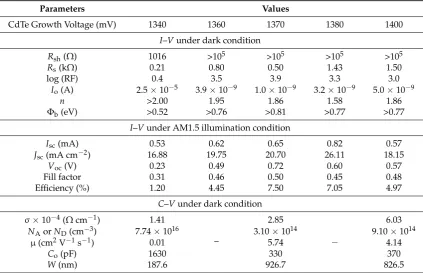
Table 2. Summary of device parameters obtained from I–V (both under illuminated and dark conditions) andC–V(dark condition) for simple CdS/CdTe-based solar cells grown at different growth voltages in the vicinity ofVi= 1370 mV.
Parameters Values
CdTe Growth Voltage (mV) 1340 1360 1370 1380 1400
I–Vunder dark condition
Rsh(Ω) 1016 >105 >105 >105 >105
Rs(kΩ) 0.21 0.80 0.50 1.43 1.50
log (RF) 0.4 3.5 3.9 3.3 3.0
Io(A) 2.5×10⁻⁵ 3.9×10⁻⁹ 1.0×10⁻⁹ 3.2×10⁻⁹ 5.0×10⁻⁹
n >2.00 1.95 1.86 1.58 1.86
Φb(eV) >0.52 >0.76 >0.81 >0.77 >0.77
I–Vunder AM1.5 illumination condition
Isc(mA) 0.53 0.62 0.65 0.82 0.57
Jsc(mA cm−2) 16.88 19.75 20.70 26.11 18.15
Voc(V) 0.23 0.49 0.72 0.60 0.57
Fill factor 0.31 0.46 0.50 0.45 0.48
Efficiency (%) 1.20 4.45 7.50 7.05 4.97
C–Vunder dark condition
σ×10−4(Ωcm−1) 1.41
–
2.85
−
6.03
NAorND(cm−3) 7.74×10¹⁶ 3.10×10¹⁴ 9.10×10¹⁴ µ(cm2V−1s−1) 0.01 5.74 4.14
Co(pF) 1630 330 370
W(nm) 187.6 926.7 826.5
It is well known that intrinsic CdS is n-type and remainsn-type due to the inherent defect as a result of the presence of S vacancies and Cd interstitials in the crystal lattice of the deposited CdS layers [93]. The devices are fabricated by incorporating CdTe deposited at the vicinity of the transition voltage (Vi) from p-type to n-type CdTe or vice versa. Electroplated CdTe can either be p-type (when Te rich) or n-type (when Cd rich) material under as-deposited condition. Retention or transition of electrical conduction type is possible after cadmium chloride treatment. It is noteworthy that the conversion of the electrical conduction type after post-growth treatment may be attributed to the doping effect as a result of the heat treatment temperature, duration of treatment, initial atomic composition of Cd and Te, the concentration of CdCl2utilised in treatment, defect structure present in the starting CdTe layer, and the material’s initial conductivity type as documented in the literature [40,41,94]. Therefore depending on the final electrical conduction type, the possible device configurations are possible, and the analysis of device results must be performed with extreme care.
Table2summarises the results of CdS/CdTe solar cells made with CdTe layers grown in the vicinity ofVi= 1370 mV. Below theVi, the CdTe layers are p-type and therefore the devices made are p-n junctions (see Figure6a). Above theVi,the CdTe layers are n-type and hence the device structures are n-n+Schottky barrier (see Figure6b). As shown in Table2, the devices fabricated with n-CdTe performs better than those made with p-CdTe layers.
CdTe-based devices assuming p-CdTe in CdS/CdTe devices has been documented in the literature [27,95]. But based on recent observations, the incorporation of Cd-rich CdTe absorber layers produce high efficiencies. These effects have been independently observed and reported [96,97] and mainly attributed to the reduced defects in Cd-rich CdTe (the layers are deposited using physical deposition processes).
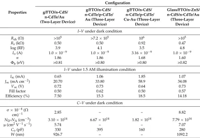
Table 3.Summary of device parameters obtained fromI–V(both under illuminated and dark conditions) andC–V(dark condition) for glass/FTO/n-CdS/n-CdTe/Au and glass/FTO/n-ZnS/n-CdS/n-CdTe/Au solar cells.
Properties
Configuration
g/FTO/n-CdS/ n-CdTe/Au (Two-Layer Device)
g/FTO/n-CdS/ n-CdTe/p-CdTe/ Au (Three-Layer
Device)
g/FTO/n-CdS/ n-CdTe/p-CdTe/ Cu-Au (Three-Layer
Device)
Glass/FTO/n-ZnS/ n-CdS/n-CdTe/Au
(Three-Layer Device)
I–Vunder dark condition
Rsh(Ω) >105 >7.2×10⁵ 106 >105
Rs(kΩ) 0.50 0.50 0.92 0.47
log (RF) 3.9 4.1 3.5 4.8
Io(A) 1.0×10⁻⁹ 1.0×10⁻⁹ 3.16×10⁻⁹ 1.0×10⁻⁹
n 1.86 1.86 1.68 1.60
Φb(eV) >0.81 >0.80 >0.80 >0.82 I–Vunder 1.5 AM illumination condition
Isc(mA) 0.65 1.06 1.85 1.07
Jsc(mA cm−2) 20.70 33.80 58.9 34.08
Voc(V) 0.72 0.73 0.64 0.73
Fill factor 0.50 0.62 0.50 0.57
Efficiency (%) 7.50 15.3 18.5 14.18
C–Vunder dark condition
σ×10−4(Ω
cm)−1 2.85 – – 8.82
ND-NA(cm−3) 3.10×10¹⁴ 6.67×10¹⁴ 1.82×10¹⁴ 7.79×10¹⁴
µ(cm2V−1s−1) 5.74 – – 7.07
Co(pF) 330 395 160 280
W(nm) 926.7 – – 1092.2
6. Conclusions
This work describes electroplating as a robust material deposition technique with wide applications ranging from surface protection to large-area electronics and nano-technology while focusing on semiconductor deposition. The manuscript also reviews the pros and cons of electroplating techniques. The effect of growth parameters such as temperature, pH, stirring rate, precursor, solvent and cathodic voltage, and post-growth heat treatments of the deposited were iterated. The capability of electroplated material to be comparable and possibly superior to semiconductor materials grown using other cash intensive techniques are also highlighted with experimental evidence. Electroplated materials can be applicable in large-area devices such as photovoltaic solar panels and large-area display panels in which intricate shapes are required. Bandgap grading, alteration of elemental composition, and different conductivity type are also possible intrinsically with a change in the cathodic voltage. Other advantages such as columnar growth of nanorods which are tightly packed and normal to the substrate could trigger many new applications in the nanotechnology area.
Funding:This research received no external funding
Acknowledgments: The authors acknowledge the support of Sheffield Hallam University and Ekiti State University.
Conflicts of Interest:The authors declare no conflict of interest.
References
1. Lincot, D. Electrodeposition of semiconductors.Thin Solid Films2005,487, 40–48. [CrossRef]
Coatings2018,8, 262 13 of 17
3. Panicker, M.P.R. Cathodic deposition of CdTe from aqueous electrolytes.J. Electrochem. Soc.1978,125, 566–572. [CrossRef]
4. Danaher, W.J.; Lyons, L.E.; Morris, G.C. Some properties of thin films of chemically deposited cadmium sulphide.Sol. Energy Mater.1985,12, 137–148. [CrossRef]
5. Basol, B.M. High-efficiency electroplated heterojunction solar cell.J. Appl. Phys.1984,55, 601–603. [CrossRef] 6. Neumann-Spallart, M.; Königstein, C. Electrodeposition of zinc telluride.Thin Solid Films1995,265, 33–39.
[CrossRef]
7. Sanders, B.W.; Kitai, A.H. The electrodeposition of thin film zinc sulphide from thiosulphate solution.
J. Cryst. Growth1990,100, 405–410. [CrossRef]
8. Izaki, M. Electrolyte optimization for cathodic growth of zinc oxide films.J. Electrochem. Soc.1996,143, L53–L55. [CrossRef]
9. Dharmadasa, I.M.; Burton, R.P.; Simmonds, M. Electrodeposition of CuInSe2layers using a two-electrode system
for applications in multi-layer graded bandgap solar cells.Sol. Energy Mater. Sol. Cells2006,90, 2191–2200. [CrossRef]
10. Al-Bassam, A.A.I. Electrodeposition of CuInSe2thin films and their characteristics.Phys. B Condens. Matter 1999,266, 192–197. [CrossRef]
11. Dharmadasa, I.M. Latest developments in CdTe, CuInGaSe2and GaAs/AlGaAs thin film PV solar cells. Curr. Appl. Phys.2009,9, e2–e6. [CrossRef]
12. McHardy, J.; Ludwig, F.Electrochemistry of Semiconductors and Electronics: Processes and Devices; William Andrew: Norwich, NY, USA, 1992; ISBN 9780815513018.
13. Ojo, A.A.; Dharmadasa, I.M. 15.3% efficient graded bandgap solar cells fabricated using electroplated CdS and CdTe thin films.Sol. Energy2016,136, 10–14. [CrossRef]
14. Dharmadasa, I.M.; Bingham, P.; Echendu, O.K.; Salim, H.I.; Druffel, T.; Dharmadasa, R.; Sumanasekera, G.; Dharmasena, R.; Dergacheva, M.B.; Mit, K.; et al. Fabrication of CdS/CdTe-based thin film solar cells using an electrochemical technique.Coatings2014,4, 380–415. [CrossRef]
15. Pandey, J. Solar cell harvesting: Green renewable technology of future introduction.Int. J. Adv. Res. Eng. Appl. Sci.2015,4, 93–103.
16. Dennison, S. Dopant and impurity effects in electrodeposited CdS/CdTe thin films for photovoltaic applications.J. Mater. Chem.1994,4, 41–46. [CrossRef]
17. Zanio, K.Semiconductors and Semimetals; Academic Press: Cambridge, MA, USA, 1978.
18. Meulenkamp, E.A.; Peter, L.M. Mechanistic aspects of the electrodeposition of stoichiometric CdTe on semiconductor substrates.J. Chem. Soc. Trans.1996,92, 4077–4082. [CrossRef]
19. Shenouda, A.Y.; El Sayed, M. Electrodeposition, characterization and photo electrochemical properties of CdSe and CdTe.Ain Shams Eng. J.2015,6, 341–346. [CrossRef]
20. Atapattu, H.Y.R.; De Silva, D.S.M.; Pathiratne, K.A.S.; Dharmadasa, I.M. Effect of stirring rate of electrolyte on properties of electrodeposited CdS layers.J. Mater. Sci. Mater. Electron.2016,27, 5415–5421. [CrossRef] 21. Ojo, A.A.; Salim, H.I.; Olusola, O.I.; Madugu, M.L.; Dharmadasa, I.M. Effect of thickness: A case study of
electrodeposited CdS in CdS/CdTe based photovoltaic devices.J. Mater. Sci. Mater. Electron.2017,28, 3254–3263. [CrossRef]
22. De Alwis, A.C.S.; Atapattu, H.Y.R.; De Silva, D.S.M. Influence of the type of conducting glass substrate on the properties of electrodeposited CdS and CdTe thin films.J. Mater. Sci. Mater. Electron.2018. [CrossRef] 23. Dharmadasa, I.; Madugu, M.; Olusola, O.; Echendu, O.; Fauzi, F.; Diso, D.; Weerasinghe, A.; Druffel, T.;
Dharmadasa, R.; Lavery, B.; et al. Electroplating of CdTe thin films from cadmium sulphate precursor and comparison of layers grown by 3-electrode and 2-electrode systems.Coatings2017,7, 17. [CrossRef] 24. Echendu, O.K.; Okeoma, K.B.; Oriaku, C.I.; Dharmadasa, I.M. Electrochemical deposition of CdTe
semiconductor thin films for solar cell application using two-electrode and three-electrode configurations: A comparative study.Adv. Mater. Sci. Eng.2016,2016, 3581725. [CrossRef]
25. Sun, J.; Zhong, D.K.; Gamelin, D.R. Composite photoanodes for photoelectrochemical solar water splitting.
Energy Environ. Sci.2010,3, 1252–1261. [CrossRef]
27. Das, S.K.; Morris, G.C. Preparation and characterisation of electrodepositedn-CdS/p-CdTe thin film solar cells.Sol. Energy Mater. Sol. Cells1993,28, 305–316. [CrossRef]
28. Daniel, L.; Michel, F.; Hubert, C. Chemical Deposition of Chalcogenide Thin Films from Solution. InAdvances in Electrochemical Science and Engineering; Alkire, R.C., Kolb, D.M., Eds.; Wiley-Blackwell: Hoboken, NJ, USA, 2008; pp. 165–235. ISBN 9783527616800.
29. Ojo, A.A.; Dharmadasa, I.M. Investigation of electronic quality of electrodeposited cadmium sulphide layers from thiourea precursor for use in large area electronics.Mater. Chem. Phys.2016,180, 14–28. [CrossRef] 30. Salim, H.I.; Olusola, O.I.; Ojo, A.A.; Urasov, K.A.; Dergacheva, M.B.; Dharmadasa, I.M. Electrodeposition
and characterisation of CdS thin films using thiourea precursor for application in solar cells.J. Mater. Sci. Mater. Electron.2016,27, 6786–6799. [CrossRef]
31. Chaure, N.B.; Samantilleke, A.P.; Dharmadasa, I.M. The effects of inclusion of iodine in CdTe thin films on material properties and solar cell performance.Sol. Energy Mater. Sol. Cells2003,77, 303–317. [CrossRef] 32. Paterson, R.; Anderson, J.; Anderson, S.S. Lutfullah transport in aqueous solutions of group IIB metal
salts at 298.15 K. Part 2—Interpretation and prediction of transport in dilute solutions of cadmium iodide: An irreversible thermodynamic analysis. J. Chem. Soc. Faraday Trans. 1 Phys. Chem. Condens. Phases 1977,73, 1773–1778. [CrossRef]
33. Paterson, R.; Devine, C. Transport in aqueous solutions of group IIB metal salts. Part 7—Measurement and prediction of isotopic diffusion coefficients for iodide in solutions of cadmium iodide.J. Chem. Soc. Faraday Trans. 1 Phys. Chem. Condens. Phases1980,76, 1052–1061. [CrossRef]
34. Dharmadasa, I.M.; Echendu, O.K.; Fauzi, F.; Abdul-Manaf, N.A.; Olusola, O.I.; Salim, H.I.; Madugu, M.L.; Ojo, A.A. Improvement of composition of CdTe thin films during heat treatment in the presence of CdCl2. J. Mater. Sci. Mater. Electron.2017,28, 2343–2352. [CrossRef]
35. Dharmadasa, I.M.; Echendu, O.K.; Fauzi, F.; Abdul-Manaf, N.A.; Salim, H.I.; Druffel, T.; Dharmadasa, R.; Lavery, B. Effects of CdCl2treatment on deep levels in CdTe and their implications on thin film solar cells:
A comprehensive photoluminescence study.J. Mater. Sci. Mater. Electron.2015,26, 4571–4583. [CrossRef] 36. Samantilleke, A.P.; Boyle, M.H.; Young, J.; Dharmadasa, I.M. Electrodeposition ofn-type andp-type ZnSe
thin films for applications in large area optoelectronic devices.J. Mater. Sci. Mater. Electron.1998,9, 231–235. [CrossRef]
37. Wellings, J.S.; Chaure, N.B.; Heavens, S.N.; Dharmadasa, I.M. Growth and characterisation of electrodeposited ZnO thin films.Thin Solid Films2008,516, 3893–3898. [CrossRef]
38. Madugu, M.L.; Olusola, O.I.-O.; Echendu, O.K.; Kadem, B.; Dharmadasa, I.M. Intrinsic doping in electrodeposited ZnS thin films for application in large-area optoelectronic devices. J. Electron. Mater. 2016,45, 2710–2717. [CrossRef]
39. Abdul-Manaf, N.A.; Echendu, O.K.; Fauzi, F.; Bowen, L.; Dharmadasa, I.M. Development of polyaniline using electrochemical technique for plugging pinholes in cadmium sulfide/cadmium telluride solar cells.
J. Electron. Mater.2014,43, 4003–4010. [CrossRef]
40. Salim, H.I.; Patel, V.; Abbas, A.; Walls, J.M.; Dharmadasa, I.M. Electrodeposition of CdTe thin films using nitrate precursor for applications in solar cells.J. Mater. Sci. Mater. Electron.2015,26, 3119–3128. [CrossRef] 41. Abdul-Manaf, N.A.; Salim, H.I.; Madugu, M.L.; Olusola, O.I.; Dharmadasa, I.M. Electro-plating and characterisation of CdTe thin films using CdCl2as the cadmium source. Energies2015,8, 10883–10903.
[CrossRef]
42. Dharmadasa, I.M.; Chaure, N.B.; Tolan, G.J.; Samantilleke, A.P. Development of p+, p, i, n, and n+-Type CuInGaSe2layers for applications in graded bandgap multilayer thin-film solar cells.J. Electrochem. Soc. 2007,154, H466–H471. [CrossRef]
43. Olusola, O.I.; Echendu, O.K.; Dharmadasa, I.M. Development of CdSe thin films for application in electronic devices.J. Mater. Sci. Mater. Electron.2015,26, 1066–1076. [CrossRef]
44. Madugu, M.L.; Bowen, L.; Echendu, O.K.; Dharmadasa, I.M. Preparation of indium selenide thin film by electrochemical technique.J. Mater. Sci. Mater. Electron.2014,25, 3977–3983. [CrossRef]
45. Olusola, O.I.; Madugu, M.L.; Abdul-Manaf, N.A.; Dharmadasa, I.M. Growth and characterisation of n- and p-type ZnTe thin films for applications in electronic devices.Curr. Appl. Phys.2016,16, 120–130. [CrossRef]
46. Abdul-Manaf, N.A.; Weerasinghe, A.R.; Echendu, O.K.; Dharmadasa, I.M. Electro-plating and
characterisation of cadmium sulphide thin films using ammonium thiosulphate as the sulphur source.
Coatings2018,8, 262 15 of 17
47. Diso, D.G.; Muftah, G.E.A.; Patel, V.; Dharmadasa, I.M. Growth of CdS layers to develop all-electrodeposited CdS/CdTe thin-film solar cells.J. Electrochem. Soc.2010,157, H647–H651. [CrossRef]
48. Ben Nasr, T.; Kamoun, N.; Kanzari, M.; Bennaceur, R. Effect of pH on the properties of ZnS thin films grown by chemical bath deposition.Thin Solid Films2006,500, 4–8. [CrossRef]
49. Wu, W.; Eliaz, N.; Gileadi, E. The effects of pH and temperature on electrodeposition of Re-Ir-Ni coatings from aqueous solutions.J. Electrochem. Soc.2014,162, D20–D26. [CrossRef]
50. Kum, M.C.; Yoo, B.Y.; Rheem, Y.W.; Bozhilov, K.N.; Chen, W.; Mulchandani, A.; Myung, N.V. Synthesis and characterization of cadmium telluride nanowire.Nanotechnology2008,19, 325711. [CrossRef] [PubMed] 51. Londhe, P.U.; Chaure, N.B. Effect of pH on electrodeposited ZnO thin films.AIP Conf. Proc.2012,1447, 671–672.
[CrossRef]
52. Kafi, F.S.B.; Jayathileka, K.M.D.C.; Wijesundera, R.P.; Siripala, W. Effect of bath pH on interfacial properties of electrodeposited n-Cu2O films.Phys. Status Solidi b2018,255, 1700541. [CrossRef]
53. Rami, M.; Benamar, E.; Fahoume, M.; Ennaoui, A. Growth analysis of electrodeposited CdS on ITO coated glass using atomic force microscopy.Phys. Status Solidi a1999,172, 137–147. [CrossRef]
54. Haerifar, M.; Zandrahimi, M. Effect of current density and electrolyte pH on microstructure of Mn–Cu electroplated coatings.Appl. Surf. Sci.2013,284, 126–132. [CrossRef]
55. Hillel, D. Water properties. InEncyclopedia of Soils in the Environment; Academic Press: Cambridge, MA, USA, 2005; pp. 290–300.
56. Huang, C.; Chuang, C.; Hsu, F.; Li, K. The properties of ZnO deposits electroplated on an ITO glass substrate with direct- and pulse currents.Int. J. Mater. Mech. Manuf.2017,5, 1–5. [CrossRef]
57. Basol, B.M. Electrodeposited CdTe and HgCdTe solar cells.Sol. Cells1988,23, 69–88. [CrossRef]
58. Rastogi, A.C.; Balakrishnan, K.S. Growth, structure and composition of electrodeposited CdTe thin films for solar cells.Sol. Energy Mater. Sol. Cells1995,36, 121–146. [CrossRef]
59. Razmjoo, O.; Bahrololoom, M.E.; Najafisayar, P. The effect of current density on the composition, structure, morphology and optical properties of galvanostatically electrodeposited nanostructured cadmium telluride films.Ceram. Int.2017,43, 121–127. [CrossRef]
60. Donghwan, K.; Pozder, S.; Zhu, Y.; Trefny, J.U. Polycrystalline thin film CdTe solar cells fabricated by electrodeposition. In Proceedings of the 1994 IEEE 1st World Conference on Photovoltaic Energy Conversion—WCPEC (A Joint Conference of PVSC, PVSEC and PSEC), Waikoloa, HI, USA, 5–9 December 2014; pp. 334–337.
61. Ojo, A.A. Engineering of Electroplated Materials for Multilayer Next Generation Graded Bandgap Solar Cells. Ph.D. Thesis, Sheffield Hallam University, Sheffield, UK, 10 April 2017.
62. Ojo, A.A.; Dharmadasa, I.M. Analysis of electrodeposited CdTe thin films grown using cadmium chloride precursor for applications in solar cells.J. Mater. Sci. Mater. Electron.2017,28, 14110–14120. [CrossRef] 63. Ng, J.H.G.; Record, P.M.; Shang, X.; Wlodarczyk, K.L.; Hand, D.P.; Schiavone, G.; Abraham, E.; Cummins, G.;
Desmulliez, M.P.Y. Optimised co-electrodeposition of Fe–Ga alloys for maximum magnetostriction effect.
Sensors Actuators A Phys.2015,223, 91–96. [CrossRef]
64. Allongue, P.; Souteyrand, E. Metal electrodeposition on semiconductors. J. Electroanal. Chem. Interfacial Electrochem.1990,286, 217–237. [CrossRef]
65. Ojo, A.A.; Dharmadasa, I.M. Effect of gallium doping on the characteristic properties of polycrystalline cadmium telluride thin film.J. Electron. Mater.2017,46, 5127–5135. [CrossRef]
66. Akai, T.; Kuraoka, K.; Chen, D.; Yamamoto, Y.; Shirakami, T.; Urabe, K.; Yazawa, T. leaching behavior of sodium from fine particles of soda-lime-silicate glass in acid solution.J. Am. Ceram. Soc.2005,88, 2962–2965. [CrossRef]
67. Dharmadasa, I.M.; Ojo, A.A. Unravelling complex nature of CdS/CdTe based thin film solar cells.J. Mater. Sci. Mater. Electron.2017,28, 16598–16617. [CrossRef]
68. Chaure, N.B.; Young, J.; Samantilleke, A.P.; Dharmadasa, I.M. Electrodeposition of p-i-n type CuInSe2
multilayers for photovoltaic applications.Sol. Energy Mater. Sol. Cells2004,81, 125–133. [CrossRef] 69. Chaure, N.B.; Samantilleke, A.P.; Burton, R.P.; Young, J.; Dharmadasa, I.M. Electrodeposition ofp+,p,i,n
70. Delsol, T.; Samantilleke, A.P.; Chaure, N.B.; Gardiner, P.H.; Simmonds, M.; Dharmadasa, I.M. Experimental study of graded bandgap Cu(InGa)(SeS)2thin films grown on glass/molybdenum substrates by selenization
and sulphidation.Sol. Energy Mater. Sol. Cells2004,82, 587–599. [CrossRef]
71. Ojo, A.A.; Dharmadasa, I.M. The effect of fluorine doping on the characteristic behaviour of CdTe.
J. Electron. Mater.2016,45, 5728–5738. [CrossRef]
72. Ojo, A.A.; Dharmadasa, I.M. Electrodeposition of fluorine-doped cadmium telluride for application in photovoltaic device fabrication.Mater. Res. Innov.2015,19, 470–476. [CrossRef]
73. Razykov, T.M.; Ferekides, C.S.; Morel, D.; Stefanakos, E.; Ullal, H.S.; Upadhyaya, H.M. Solar photovoltaic electricity: Current status and future prospects.Prog. Sol. Energy2011,85, 1580–1608. [CrossRef]
74. Kern, W.; Schuegraf, K.K. Deposition Technologies and Applications: Introduction and Overview. InHandbook of Thin Film Deposition Processes and Techniques; Seshan, K., Ed.; William Andrew: Norwich, NY, USA, 2001; pp. 11–43.
75. Dharmadasa, I.M.; Samantilleke, A.P.; Young, J.; Boyle, M.H.; Bacewicz, R.; Wolska, A. Electrodeposited
p-type andn-type ZnSe layers for light emitting devices and multi-layer tandem solar cells.J. Mater. Sci. Mater. Electron.1999,10, 441–445. [CrossRef]
76. Ferekides, C.S.; Marinskiy, D.; Viswanathan, V.; Tetali, B.; Palekis, V.; Selvaraj, P.; Morel, D.L. High efficiency CSS CdTe solar cells.Thin Solid Films2000,361–362, 520–526. [CrossRef]
77. Bosio, A.; Romeo, N.; Mazzamuto, S.; Canevari, V. Polycrystalline CdTe thin films for photovoltaic applications.Prog. Cryst. Growth Charact. Mater.2006,52, 247–279. [CrossRef]
78. Cunningham, D.; Rubcich, M.; Skinner, D. Cadmium telluride PV module manufacturing at BP solar.
Prog. Photovoltaics Res. Appl.2002,10, 159–168. [CrossRef]
79. Turner, A.K.; Woodcock, J.M.; Özsan, M.E.; Cunningham, D.W.; Johnson, D.R.; Marshall, R.J.; Mason, N.B.; Oktik, S.; Patterson, M.H.; Ransome, S.J. BP solar thin film CdTe photovoltaic technology.Sol. Energy Mater. Sol. Cells1994,35, 263–270. [CrossRef]
80. Ehl, R.G.; Ihde, A.J. Faraday’s electrochemical laws and the determination of equivalent weights.
J. Chem. Educ.1954,31, 226. [CrossRef]
81. Ojo, A.A.; Dharmadasa, I.M. Optimisation of pH of the CdCl2+ Ga2(SO4)3activation step of CdS/CdTe
based thin-film solar cells.Sol. Energy2018,170, 398–405. [CrossRef]
82. Dharmadasa, I.M. Review of the CdCl2Treatment used in CdS/CdTe thin film solar cell development and
new evidence towards improved understanding.Coatings2014,4, 282–307. [CrossRef]
83. Ojo, A.A.; Dharmadasa, I.M. Optimisation of pH of cadmium chloride post-growth-treatment in processing CDS/CDTE based thin film solar cells.J. Mater. Sci. Mater. Electron.2017,28, 7231–7242. [CrossRef] 84. Hajimammadov, R.; Fathi, N.; Bayramov, A.; Khrypunov, G.; Klochko, N.; Li, T. Effect of “CdCl2Treatment”
on Properties of CdTe-based solar cells prepared by physical vapor deposition and close-spaced sublimation methods.Jpn. J. Appl. Phys.2011,50, 05FH01. [CrossRef]
85. Rios-Flores, A.; Peña, J.L.; Castro-Peña, V.; Ares, O.; Castro-Rodríguez, R.; Bosio, A. A study of vapor CdCl2
treatment by CSS in CdS/CdTe solar cells.Sol. Energy2010,84, 1020–1026. [CrossRef]
86. Schiavone, G.; Murray, J.; Smith, S.; Desmulliez, M.P.Y.; Mount, A.R.; Walton, A.J. A wafer mapping technique for residual stress in surface micromachined films.J. Micromech.Microeng.2016,26, 095013. [CrossRef] 87. Schiavone, G.; Murray, J.; Perry, R.; Mount, A.; Desmulliez, M.; Walton, A. Integration of electrodeposited
Ni-Fe in MEMS with low-temperature deposition and Etch processes.Materials2017,10, 323. [CrossRef] [PubMed]
88. Dharmadasa, I.M.; Echendu, O.K. Electrodeposition of electronic materials for applications in macroelectronic- and nanotechnology-based devices. InEncyclopedia of Applied Electrochemistry; Kreysa, G., Ota, K.-i., Savinell, R.F., Eds.; Springer: New York, NY, USA, 2014; pp. 680–691.
89. Bhattacharya, R.N.; Oh, M.-K.; Kim, Y. CIGS-based solar cells prepared from electrodeposited precursor films.Sol. Energy Mater. Sol. Cells2012,98, 198–202. [CrossRef]
90. Echendu, O.K.; Fauzi, F.; Weerasinghe, A.R.; Dharmadasa, I.M. High short-circuit current density CdTe solar cells using all-electrodeposited semiconductors.Thin Solid Films2014,556, 529–534. [CrossRef]
91. Ojo, A.A.; Dharmadasa, I.M. Analysis of the electronic properties of all-electroplated ZnS, CdS and CdTe graded bandgap photovoltaic device configuration.Sol. Energy2017,158, 721–727. [CrossRef]
Coatings2018,8, 262 17 of 17
93. Sathaye, S.D.; Sinha, A.P.B. Studies on thin films of cadmium sulphide prepared by a chemical deposition method.Thin Solid Films1976,37, 15–23. [CrossRef]
94. Basol, B.M. Processing high efficiency CdTe solar cells.Int. J. Sol. Energy1992,12, 25–35. [CrossRef] 95. Woodcock, J.M.; Turner, A.K.; Ozsan, M.E.; Summers, J.G. Thin film solar cells based on electrodeposited
CdTe. In Proceedings of the Conference Record of the Twenty-Second IEEE Photovoltaic Specialists Conference, Las Vegas, NV, USA, 7–11 October 1991; pp. 842–847.
96. Reese, M.O.; Perkins, C.L.; Burst, J.M.; Farrell, S.; Barnes, T.M.; Johnston, S.W.; Kuciauskas, D.; Gessert, T.A.; Metzger, W.K. Intrinsic surface passivation of CdTe.J. Appl. Phys.2015,118, 155305. [CrossRef]
97. Burst, J.M.; Duenow, J.N.; Albin, D.S.; Colegrove, E.; Reese, M.O.; Aguiar, J.A.; Jiang, C.-S.; Patel, M.K.; Al-Jassim, M.M.; Kuciauskas, D.; et al. CdTe solar cells with open-circuit voltage breaking the 1 V barrier.
Nat. Energy2016,1, 16015. [CrossRef]