A template-based methodology for efficient
microprocessor and FPGA accelerator co-design
KRITIKAKOU, Angeliki, CATTHOOR, Francky, ATHANASIOU, George,
KELEFOURAS, Vasileios <http://orcid.org/0000-0001-9591-913X> and
GOUTIS, Costas E.
Available from Sheffield Hallam University Research Archive (SHURA) at:
http://shura.shu.ac.uk/18350/
This document is the author deposited version. You are advised to consult the
publisher's version if you wish to cite from it.
Published version
KRITIKAKOU, Angeliki, CATTHOOR, Francky, ATHANASIOU, George,
KELEFOURAS, Vasileios and GOUTIS, Costas E. (2013). A template-based
methodology for efficient microprocessor and FPGA accelerator co-design. In: 2012
International Conference on Embedded Computer Systems (SAMOS). IEEE, 15-22.
Copyright and re-use policy
See
http://shura.shu.ac.uk/information.html
A Template-based Methodology for Efficient
Microprocessor and FPGA Accelerator Co-Design
Angeliki Kritikakou
∗, Francky Catthoor
†, George S. Athanasiou
∗, Vasilios Kelefouras
∗and Costas Goutis
∗∗Dep. Electrical & Computer Engineering, Univ. of Patras, Patras, Greece, 26500. Email: [email protected] † Inter-university Micro-Electronics (IMEC) & Dep. Electrical Engineering (ESAT), KULeuven, Leuven, Belgium
Abstract—Embedded applications usually require
Soft-ware/Hardware (SW/HW) designs to meet the hard timing con-straints and the required design flexibility. Exhaustive exploration for SW/HW designs is a very time consuming task, while the ad-hoc approaches and the use of partially automatic tools usually lead to less efficient designs. To support a more efficient co-design process for FPGA platforms we propose a systematic methodology to map an application to SW/HW platform with a custom HW accelerator and a microprocessor core. The methodology mapping steps are expressed through parametric templates for the SW/HW Communication Organization, the Foreground (FG) Memory Management and the Data Path (DP) Mapping. Several performance-area tradeoff design Pareto points are produced by instantiating the templates. A real-time bio-imaging application is mapped on a FPGA to evaluate the gains of our approach, i.e. 44,8%on performance compared with pure SW designs and 58%on area compared with pure HW designs.
I. INTRODUCTION
Embedded time applications usually have hard real-time constraints. When these are not met, alternative designs should be composed. The performance can be further im-proved, when the critical application tasks are executed in custom and application specific HW designs. However, HW designs have a high design cost and their flexibility remains very limited, even when they are made partly configurable. The SW approaches provide the required flexibility for a wide range of applications, but at the cost of reduced performance. A hybrid approach is a promising solution, as it combines the advantages of both designs by balancing the flexibility of the SW implementation with the performance of custom HW [2]. Such hybrid approaches require an efficient exploration of the application domain. This is achieved by identifying the application parts which are meaningful to be potentially designed in a HW component, by analyzing the tradeoff between the custom HW complexity and the obtained gain and by providing an effective and easy to be programmed system [2]. Existing design tools offer a partially automatic customization of soft microprocessors. These tools usually require a high exploration time as they may explore a wide range of design instances, which are, however, restricted and focused on a relatively limited exploration area (Section II).
The results were co-financed by: Public Welfare Foundation “Propondis” research funds, Hellenic and European Regional Development Fund (ERDF) under ESPA 2007-2013 (MICRO2-SE-G) and European Social Fund (ESF) and Greek national funds (Heracleitus II-NSRF). The machine vision algo-rithm and SW model were patented by Micro2gen [1].
When the application does not match very well with the explored area, this approach leads to suboptimal designs. A very broad Design Space Exploration (DSE) corresponds to a very difficult and time consuming task due to the high number of SW and HW design parameters. Hence, the designers usually create hybrid designs by following ad-hoc or trial and error ways based on their expertise, which require costly design iterations (Section II). Hence, a systematic way is highly desired to support the complete DSE for efficient SW/HW design within an acceptable search time [3].
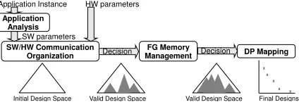
The first main contribution to achieve this goal is a stepwise template-based methodology to produce a Pareto curve with performance-area tradeoff points for mapping an application to a SW/HW design. The DSE is performed within acceptable search time since only the valid and promising part is ex-plored based on an efficient and scalable what-if analysis. The mapping process is split into sequential steps connected with uni-directional propagation of design constraints used to prune incompatible options in the next mapping steps. The steps are the SW/HW Communication Organization, the FG Memory Management (the memory attached to the data path) and the DP mapping and are described by parameterized templates. The application and the platform instance constraints are propagated to the steps to further prune suboptimal options. The main design objectives are to minimize area and, thus, reduce energy consumption in FPGAs, while meeting all real-time application constraints. The Pareto Points are derived by instantiating the parameters of the proposed templates with specific values. In this way, efficient exploration is achieved from the early mapping steps of the co-design process. Our second main contribution is to demonstrate how the proposed methodology is applied in a real-time bio-imaging application of a microfluidic-based FPGA device and produces interesting Pareto points between the pure SW and HW approaches.
The paper is organized as follows: Section II presents existing design approaches and tools, including the few really systematic ones. Section III describes the proposed method-ology. Section IV presents a demonstration of applying our methodology to a real-time bio-imaging application and the evaluation results. Section V concludes the current study.
II. RELATEDWORK
HW components supporting hybrid SW/HW implementations. However, the tools and the development methodologies are mainly inadequate to support the efficient mapping of appli-cations to (re-)configurable embedded systems [4].
Several design tools exist to partially customize soft micro-processors. For instance, Synopsys Synphony C compiler [5] creates accelerators from sequential code. CriticalBlue cas-cade [6] is an automated co-processors synthesis solution. Tosca, Cosmos, Handel-C and ImpulseC (a survey is available in [7]), provide RTL extensions to C for FPGA design, but they provide less efficient results than custom HW designs. The tools identify automated design flows and implement the custom instructions, but they also require specification of new HW resources and rewriting part of the application [2]. In [8], the compiler generates custom instructions by finding and adding the instruction data paths that can be reused across similar code pieces to the customizable processor. However, the exploration and verification time induces a significant overhead [2] and the design may remain quite suboptimal [8]. These approaches usually require a high exploration time as they apply a very extensive (or nearly exhaustive) DSE on a relatively limited part of the design space with costly design iterations. They typically restrict the supported options for the communication/connection of components and the FG memory organization, excluding potentially promising options of the unexplored design space. When the application does not match very well with the part of the overall design space selected for further exploration, the tools can easily produce sub-optimal solutions. To improve the hybrid design process, effort from the designers is required. The alternative is a very broad DSE which involves a very difficult and time consuming task due to the high number of SW and HW parameters [9].
The designers propose designs for the specific application instances by following ad-hoc or trial and error ways which increase the costly design iterations. They propose several de-signs instantiations for their specific applications using FPGA manufactures tools, such as Xilinx EDK and Altera SOPC Builder. For instance, a specific design implementation of an object tracking co-processor has been proposed in [10] and one design implementation for an object detection application in [11]. Since substantial time and effort are required to eval-uate a design, they usually evaleval-uate few final design choices, usually the ones that can be evaluated quickly based on previous experience [12]. Hence, potentially promising options are easily overlooked. For instance, in [13] a reconfigurable HW is used as a general-purpose accelerator, where applica-tion blocks are mapped using a library of modules, partially exploring the design options as relevant details of custom units are overlooked. Ref. [14] proposes a reconfigurable unit to execute specific instructions. Its performance is up-front decided (16 operations can be simultaneously executed), which potentially removes promising designs.
Existing design methodologies mainly focus on guiding a particular step of the design process. Several methodologies address the implementation of the DP of the custom HW to improve the design objectives. For instance, a methodology
based on evolutionary Multi-Objective Optimization (MOO) is proposed to create the DP of a HW accelerator for a JPEG algorithm [15]. A generic architecture is proposed which implements the control and the DP of the custom HW either inside the microprocessor or outside, as a standalone processing element [16]. A systematic approach to extend an embedded processor with generic custom units is presented in [17]. Other methodologies focus on the application of code transformations related to the memory part. For instance, the compiler in [18] extracts loop parameters to decide un-rolling and SW pipelining. In [19] they focus on balancing memory accesses with floating point operations. Several of the DSE methodologies are mainly recursive approaches. A methodology with stochastic algorithms to search the design space is proposed in [9]. A simulated annealing approach for DSE of object detection accelerators is proposed in [20]. The Single Factor Analysis (SFA) [21] starts from a base configuration selected by the designer and changes the value of one parameter each time. The results are used to predict the optimal design. It may lead to suboptimal results when a high number of parameters and interdependencies exists. Another approach sorts the parameters based on the impact determined by the maximum parameter value change. All combinations of the first two high impact parameters are considered and the non-Pareto combinations are pruned. The process is repeated for the Pareto points and the next highest impact parameter etc. [3]. The parameters independence is used to prune the space and to derive the Pareto curve in Platune [9].
III. SYSTEMATICTEMPLATE-BASEDMETHODOLOGY
The proposed stepwise template-based methodology applies an efficient and scalable DSE for efficient mapping of an ap-plication to a HW platform from the early stages of the design process and within acceptable search time. This is achieved by incorporating both the constraints of the application and the target HW platform from the beginning of the DSE. Hence, we systematically and immediately prune suboptimal solutions from the large space based on an efficient what-if analysis.
SW/HW Communication Organization Application
Analysis
FG Memory
Management DP Mapping Application Instance HW parameters
SW parameters
Decision Decision
Final Designs Valid Design Space Valid Design Space
Initial Design Space
x x
[image:4.612.69.281.55.131.2]x x x
Fig. 1. Proposed methodology steps and constraint propagation.
In the next subsections, we describe the parameterized templates of the proposed methodology following the order that the design constraints are propagated and pruning the space (Fig. 1). Initially, a preprocessing step (Application Analysis) identifies the real-time constraints, the critical ker-nels for mapping on the FPGA and their characteristics. The analysis output and the HW constraints are propagated to the SW/HW Communication Organization step to decide the microprocessor and the custom HW connection. The result is propagated to the next step for the FG Memory Management. Finally, the result is propagated to the DP Mapping, where the final design is composed.
The design objectives is reducing the area and, thus, the energy consumption in FPGA designs (due to the number of required gates), while the real-time constraints are met. A less strict latency constraint is allowed for the application kernels to optimize the throughput. In the scope of this paper, the communication of the Background (BG) Memory, i.e. distant memories from the processing elements, is organized by the SW executed on the microprocessor, using the HW of the memory and the cache controllers of the target platform. The array accesses in SW are compiled into load/store operations and the cache controller handles the data [22].
A. Application Analysis Step
The application real-time constraints determine the deadline
D, which defines the maximum bound on the application execution time tTot, tTot ≤D. When the execution time in
pure SW design tTotSW is larger than the deadlineD, hybrid
approaches are required to meet the real-time constraints. Profiling is applied to identify the application critical parts.
1) Loops and Kernels: The execution timetiof the critical kernels is a high percentage of the total execution time. The kernel type is given by the parameterRegular. IfRegular=1, the kernel is executed in every iteration. If Regular=0, the kernel execution depends on control statements and specific values of their data. The number of cycles describe the available slack for executing the kernels and achieving real-time behavior. The cycles available for the total HW execution are given by Eq. 1, for a specific kernel HW execution by Eq. 2 and for one iteration of a specific kernel by Eq. 3:
CyclesT otHW = (tT ot−tT otSW)∗fHW (1)
Cyclesi,T otHW = ti
tT otHW ∗CyclesT otHW (2)
Cyclesi,HW =Cyclesi,T otHW
Iterations(i) (3)
The available number of cycles to transfer the data of an executed in HW Kernel in the FG memory, while real-time behavior is achieved, are given by similar equations:
CyclesT otT R= (tT ot−tT otSW)∗min(fM em, fCom/tion) (4)
Cyclesi,T otT R = ti
tT otHW ∗CyclesT otT R (5)
Cyclesi,T R= Cyclesi,T otT R Iterations (6) To select the kernel to be mapped in the custom HW, the design objectives are propagated to the application analysis. Hence, the smallest number of kernels should be selected to be mapped in one HW accelerator. The kernel with the highest rate is initially selected. When two kernels have similar rate, the kernel with the parameter Regular = 1is favored, due to the high use of the HW component, the regularity of the execution and the simpler synchronization between SW and HW components. If the total execution time still has to be reduced, the process is repeated for the similar rate data dependent kernel, the second weighted regular kernel etc.
2) Control Flow Operations: Except of the main applica-tion kernels (in the loop code), also the control flow operaapplica-tions (especially outer loop code, global conditions and initializa-tion) exist in the application. They can be executed either in the SW, i.e. parameter ExecControl =SW or implemented in the HW component,ExecControl=HW. In the first case, the complexity is moved to the microprocessor. In the second case, dedicated control and diverse FUs are inserted to the HW component. By propagating the design objectives to these two options, the control statements are selected to be executed in the microprocessor. The HW design complexity and the synchronization between components is reduced, which allows a very efficient and high-performance design of the HW DP dedicated to the execution of the highest weighted kernel operations using reduced resources. In this way, the remaining options for the control execution are pruned effectively in a Pareto optimal way, reducing the search in the exploration space. This constraint-based propagation and pruning principle is applied for the rest of the methodology, but due to paper size limitations we focus on the results of the reasoning, instead of the detailed motivation in each of the subsequent steps.
B. SW/HW Communication Organization Step
TABLE I
TRUTH TABLE OFSW/HW COMMUNICATIONORGANIZATION
Parameters Custom IP
Dependent Co-processor Control Connection
0 Not-care Not-care Standalone Custom IP
1 0 Not-care Internal FU
1 1 0 Base Co-processor
1 1 1 Control Co-processor
Data Cache
Processor Local Bus
Custom IP
Co-processor bus
SDRAM Memory
Dependent 1 0
Custom IP CoProcessor
0 1
FG Memory & DataPath
Control HW Control
Unit Custom IP
Processor
Initial Processor
Instruction Cache
(a) Parametric template.
SW/HW Organization
Fully Independent (Standalone
Custom IP)
Partially Dependent
Internal FU External Co-processor
With Control FU (Control Co-processor)
Without Control FU (Base Co-processor)
(b) Design options.
Fig. 2. SW/HW Communication Organization Step.
to control the memory in the most efficient way. The first case is less efficient due to the bus protocol bottleneck. The second case is optimal, but with higher area and design effort. When the parameter Dependent = 1, the IP partially depends on the processor. It reuses the processor resources, e.g. memory interface, reducing custom design complexity, area and energy consumption. When the custom IP is partially dependent, it can be implemented as an extension of the internal FUs of the microprocessor or as external co-processor. These options are expressed by parameter CoP rocessor. WhenCoP rocessor= 0, the custom IP is implemented as an internal FU. This implementation affects the critical path of the processor potentially reducing the processor and the custom IP performance. The implementation of the custom IP as a co-processor (CoP rocessor= 1) removes these limitations. The processor and the co-processor can execute different parts of the application at the same time. E.g. the processor can be used for the memory address generation and the accessing of data from the memory, while the co-processor executes the kernel. The communication of the processor and the co-processor is more efficient than in the Standalone Custom IP, as it is based on a quite fast interconnection, which makes this option Pareto (near-)optimal for our domain. The other options should be selected when the complexity of the design is large. A small latency (one or two cycles) is required to write(read) the data from the co-processor. The co-processor connection width is described by the parameterW idthCoConnection, which should be set to support the maximum width of transfered data.
In the co-processor implementation two further options exist for the control (loop organization, control operations and structure): it is common or different between the processor and the co-processor. When parameterControl= 0, the control of
the part executed on the processor is the same with the control of the part executed on the DP of the co-processor. In this case, the responsibility for the synchronization of the data between the two components and the correct functionality resides on the processor. This allows a more efficient, smaller area and lower energy consumption design of the co-processor (Base co-processor). This option fully meets the design objectives, so it is a Pareto (near-)optimal for simple synchronization schemes. The processor is responsible for invoking the co-processor, which executes the operations and writes back the output to the processor. If Control = 1, different control structures can exist in the processor and in the co-processor. The co-processor requires a HW Control Unit, e.g. Finite State Machine (FSM), to support the correct functionality of the DP and the communication from/to the processor. By propagating the design objectives, this option is potentially suboptimal due the increased co-processor area. However, this option is more attractive when the design synchronization is more complex, and then it should be part of the valid design space.
C. Foreground Memory Management Step
The size of the FG Memory is determined by the required data for the kernel execution: the data accessed from the BG memory (parameter Data) and the variables of the control flow, the intermediate and final results (parameterV ariables):
SizeF GM em=Data+V ariables=
=Data+Control+Intermediate+Results (7)
A BG memory access reduction can reduce the bandwidth and the energy requirements by replacing several BG accesses with FG ones. In the Pareto optimal case, the V ariablesare placed in the FG memory and Data are transfered from the BG memory. Otherwise the most used variables are maintained in the FG memory and the remaining ones are stored back to the BG memory, increasing the latency of future accesses.
The minimal data size of the FG memory should be kept reasonably low, since any size increase of the multi-port register-file leads to a non-linear increase in energy consumption per access [24] and also an increase in the overall design complexity. The SizeF GM em should be within the minimum number of the registers required to execute one kernel iteration and the maximum number of the allowed registers:M inRegs≤ SizeF GM em ≤M axRegs. The latter is determined by the obtained gain vs. the energy consump-tion and the complexity cost of an extra register. When the parameter Dependent = 0, the SizeF GM em of the custom IP should be quite large to support all the control and flow operations, increasing energy consumption and reducing the opportunities for DP parallelism. When Dependent= 1and
Coprocessor = 0, the custom IP reuses the register file of the processor, i.e. M axRegs = SizeRegF ile. When the
Coprocessor= 1, the SizeF GM em depends on theControl parameter. If the control is executed on the co-processor, the control variables have to be also stored in the FG memory.
In the optimal case where only theDataare transfered from the BG memory, the cycles required to transfer the data are:
If CyclesReqTotTR> CyclesTotTR (Eq. 4), parallelism in
the transfer should be applied to meet the real-time constraints. If CyclesReqTotTR < CyclesTotTR opportunities exist for
improvement. Based on the frequency ratio of the memory and the custom IP, we explore the options of creating a quite balanced design between the BG memory access and the DP computation. This is achieved by minimizing the possibility of stalls during the execution by unrolling the part of the design that is executed slower. The Unrolling Factor (U F) is given by the ratio of the frequency of the memory, when it is used in the most efficient way, and the frequency of the DP: U F = fHW/fMem. If U F < 1, the memory is slower
by a factor of U F from the DP, and thus parallelism should be applied to increase the memory bandwidth. If U F > 1, the DP should be unrolled by a factor of U F to execute all operations enabled by the available memory data. Applying a factor of U F increases the parameter Data and, thus, more data are accessed and stored in the FG memory, i.e.
DataUF =U F ∗Data. It also enables the reuse of the data
(RDataand Reuse Factor (RF) ) between iterations reducing the transitions to/from BG memory and the FG size. When the
U F ≥RF, data can be reused. The parameterDatais given by DataUF&RF = (U F ∗Data)−(U F −RF)∗RData.
The V ariables are affected in a similar way. Hence, the unrolling increases the CyclesReqTotTR, which should be
smaller than the available CyclesTotTR, and the maximum
bound on SizeF GM em. Based on the parameters and the propagated values from the SW/HW organization step, theU F
is determined and the loop kernel is transformed accordingly. The scheduling of the FG memory depends also on the propagated parameters. If the parameter Dependent = 0, the scheduling is determined by the transformed loop kernel in the custom IP. When Dependent = 1 and Control = 0, the scheduling is provided by the processor. When
Coprocessor = 0 the complete scheduling is performed by the compiler of the processor. When Coprocessor = 1, the processor sends the information about which kernel iteration is executed to the co-processor. Based on this information the processor determines from which registers it will read (store) the data (results) in each iteration. The FG memory scheduling of the remaining parts of this kernel, i.e. the loop structure and the control, is performed by the compiler of the processor, since they are executed on the processor. If the control is executed on the processor, the HW control unit of the co-processor determines the FG memory scheduling.
D. DP Mapping Step
The design decisions on the SW/HW Organization and the FG Memory Management affect the DP Mapping. Based on the available data read in the FG memory, the total operations which can be executed are given by Eq. 9:
T otOP s=U F∗OP s (9)
TheOP sare the operations executed in one iteration of the initial kernel and are described by the type of the operation i
and the number of that type of operations:
OP s=
T ypeOP sX
i=0
N umi. (10)
When the parameterDependent= 0, the DP of the custom IP executes both control and arithmetic operations. When
Dependent = 1 and Coprocessor = 0, the DP executes only the arithmetic operations and the control derives by the processor. When theCoprocessor= 1, the size of the DP and the executed operations are based on theControlparameter. If
Control= 1, the control is also executed on the co-processor. IfControl= 0, the operations relevant to the application and the custom IP control are executed on the processor DP and the arithmetic operations are executed on the custom IP DP.
Each operation type executed on the custom IP is evaluated based on the design objectives. In order to reduce energy consumption in FPGAs, the area should be reduced. Hence, if an operation type is characterized as costly, exploration is applied to replace it by smaller and simpler operations, which require less gates to be executed. Then, the kernel loop is transformed accordingly. In this way the area is reduced and the use of the simple resources is highly increased. The latency is increased somewhat, but this is assumed as acceptable in our target domain. The size of the DP of both the processor and the custom IP should support the maximum length of the
Data and theV ariables. Pipelining is used to break a long critical path into smaller paths increasing frequency, which, however, should be compatible with the Microblaze clock for efficient synchronization. Propagating the design objectives, pipelining of the HW accelerator should be avoided when real-time constraints are met, as it increases area and energy consumption due to the additional registers. The final DP of the custom IP is designed to execute all the operations of one new kernel iteration with the Parallel FactorP F required to meet the real-time constraints. Hence, the execution time required for the operations in the DP of the processor and the custom IP areCyclesT otOP s=T otOps∗fHW, which should
be smaller or equal to the available cycles given by Eq. 2 and Eq. 3 (Section III-A) with parameterIterationsequal to
Iterations/U F due to the propagated U F.
IV. DEMONSTRATORDESIGN
This section illustrates most of the relevant options of the proposed methodology through a demonstrator design showing how a Pareto Curve with performance-area trade-off points and a final design proposal are produced for a bioimaging application on a FPGA.
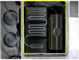
Fig. 3. The micro-fluid frame. The box is the outline of the frame and the dotted box is used by the angle detection algorithm.
uint8f[N][M];
intCoordinates, Mask[3][3], Gx[M]; Angle[M];
if(Set-up){Detect Frame position(f); Identify coordinate of pipes(f);} /*AngleDetection*/
for(row=1; row<N-1; row++){ for(col=1; col<M-1; col++){
for(rowOff=-1; rowOff≤1; rowOff++){ for(colOff=-1; colOff≤1; colOff++){
Gx[col] += f[row+rowOff][col+colOff]*Mask[rowOff+1][colOff+1];}} Gx[col] = abs(Gx[col]);
if(Gx[col]! =0){Angle[col]=90;} else{Angle[col]=0;}
if((Angle[col-1]==90)&&((Gx[col-2]<Gx[col])||(Gx[col-1]<Gx[col-2] ))){ if(Gx[col-1]>Threshold){
HoughAccumulator(row,col);}}}} LineSuppression;
FluidDetection(f);
Fig. 4. Pseudocode of the demonstrator application
algorithm requires only a vertical line (dotted box of Fig. 3) to find the angle and thus the potential frame rotation. This is achieved by applying the Canny algorithm (Fig. 4) for finding the intensity gradient of the image using a horizontal contrast 3x3 Sobel (middle column multiplicands are 0) and a Hough transform version, since the vertical line requires only computations with [−3◦,+3◦]. If the Sobel kernel’s result is an edge point, the Hough transform maps it to the Hough space and stores the results to the accumulator. The final line is detected by suppressing the neighborhood lines. The fluid coordinates derive by subtracting the micro-fluid pipes of two successive frames and by computing the centroid of the result. Our target HW platform is the Virtex-5 FPGA ML-507 Evaluation Platform with one Microblaze Soft processor at 83,33 MHz with an integer multiplier and a Floating Point FU. A SDRAM DDR2 main memory, a data and an instruction cache of 16 KB and a local memory of 32 KB are used. The data and the instructions are fetched by the HW cache controller, which does not allow SW influence so we do not incorporate this aspect in our DSE.
A. Application Analysis
The video frame ratio is 100 frames/sec, thus 10 msec are available for the total execution time of the application, i.e. the angle detection algorithm and the algorithm for the detection of the fluid fronts, tTot =tAngle+tFluid. The reference SW
implementation of the angle detection is executed in 4.31 msec by the Microblaze Soft microprocessor (Subsection IV-C). The detection of the fluid fronts’ coordinates depends on the number of fluids fronts and the frame resolution. For small
frame resolution (640x480) and 2 fluids fronts, it executes in 1.23 msec in SW. For the minimum quality application specifications (small frame and 3 edges) the average execution time is estimated at 3.9 msec and for the maximum quality (1024x1024 and 7 edges) is 7.3 msec. The total execution time of the application is tTot = 4.31+(3.9 to 7.3) msec=8.21 to
11.61 msec. Hence, real-time behavior is not always achieved since: tTotMinQ < D < tTotMaxQ. Based on application
profiling the most time consuming regular task is the angle detection algorithm and thus its critical kernels should be explored for mapping on custom HW. To safely meet the real-time constraints, the available real-time for executing the angle detection is tAngle =D−tFluid=10.0-(3.9 to 7.3) msec=6.1
to 2.7 msec, and the worst-case is considered. Based on the profiling of the angle detection algorithm, the main loop takes 68% of the total time to execute the kernel which finds the intensity gradient of the image and the kernel which creates the Hough accumulator array. The execution time of the two ker-nels is similar (31% and 33% respectively) with the intensity gradient kernel to be a regular kernel applied in every iteration of the algorithm. The application of the horizontal 3x3 Sobel mask is the 90% of the intensity kernel, so it is the first can-didate for implementation in HW (RegularSobel = 1). If the
tNewTot> D, the Hough accumulator (RegularAccHough= 0)
should be also mapped in a custom HW component. The custom IP frequency can safely be assumed to be similar to the Microblaze (when appropriate pipelining is applied), and thus the available cycles for execution of the angle detection are: CyclesTotIP=tAngle∗fHW=508,313-224,991 Cycles.
B. Final Design: An Instance of the Proposed Methodology 1) SW/HW Communication Organization: The output of the analysis step is the execution of the application on the Microblaze and the execution of the highest kernel with
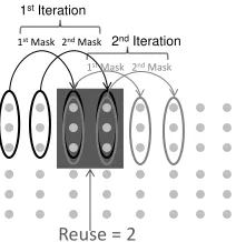
1st Mask 2nd Mask 1st Mask 2nd Mask
Reuse = 2
1st Iteration
[image:8.612.122.228.52.161.2]2nd Iteration
Fig. 5. The use of RowP ixelsin each column (circled pixels) for the execution of the two masks in each iteration. The 6 pixels are reused between two unrolled (by a factor of UF=2) iterations.
on the Microblaze, else the next Sobel masks set is executed.
2) FG Memory Management: Propagating the design op-tions from the previous steps, the data required for one execution of the horizontal contrast 3x3 Sobel mask are:
Data= 6pixels, V ariables= 2for storing the final results (Intermediate = 0, when we fully explore production con-sumption) and thusSizeF GM em = 8. The ratio of the memory and the co-processor frequency isU F=333MHz/83,33MHz=4 in the optimal case. The memory is 4 times faster than the datapath, which should be unrolled by a U F=4. In that case, one new kernel iteration requires DataUF=24
to be accessed and stored in the FG memory. With the datapath unrolling, the horizontal data reuse is explored. The pixels residing in the same column (RowP ixels=3) are reused in the mask applied, after the next column (RF=2), as depicted in Fig. 5. Hence, the final required data to be stored in the FG memory based on the equations of Section III-C are DataUF&RF=18, V ariablesUF&RF=8
and SizeFGMemUF&RF=26. Since the FG memory size
should be kept within an acceptable range (M inReqRegs=8 and M axRegs ≈ 18), the UF should be kept low. An
U F=3 requires DataUF&RF=15, V ariablesU F&RF=6 and
SizeFGMemUF&RF=21. AnU F=2 requires DataUF&RF=12,
V ariablesUF&RF=4 andSizeFGMemUF&RF=16.
Hence, the U F should be preferably 2: 12 registers are required to store the pixels of the two masks and 4 registers for storing the final results. Because U F==RF, the data reuse is explored. In each execution of the two masks only 6 new data are required to be transfered from the Microblaze to the co-processor. Since the loop control belongs to the Microblaze, it correctly sends the required pixel information. The first data of the mask, i.e. the RowP ixels of the left column (Fig. 5), are coming from previously used registers and the second data, i.e. the RowP ixels of the right column of the mask derived from the registers attached to the FSL connection. The first mask set per row requires all 12 pixels. Due to the U F and the uniformity of the accelerator execution, the first mask set is executed on the Microblaze and the first six pixels for the second set of masks are transfered to the co-processor.
3) DP Mapping: The control of the loops, the FG memory scheduling and the initialization code are executed on the Microblaze DP. The total operations executed on the
co-Fast Simplex Links (FSLs)
SDRAM
Processor Local Bus (PLB)
…
Controlers, IPs, etc...I-Cache BRAM
D-Cache BRAM
Sobel Co-Processor
+
<<REG
-<<+
+
-+
<<-<<
+
+
-compcomp
…
Custom HW
BRAM
…
Fig. 6. The HW platform architecture and the final design for the Microblaze and the HW accelerator of the demonstrator application.
processor are determined by the available data on the FG memory. The number of operations in one iteration of the initial loop are OP s = N umMUL +N umADD/SUB=9+11.
The most costly operations are the multiplications and thus the design explores the possibilities of simplifying them. Since the mask multiplicands are constant, by analyzing the constant values the number of multiplications is reduced. Multiplicands with the value of 1 are removed and the remaining ones are replaced by Shift and Add operations. Hence, OP s =
N umSHIFT+N umADD/SUB/COMP=2+6. Hence, executing
all the operations will require 4 Shift FUs (S-FUs) and 12 Add/Sub/Comp FUs (A-FUs) (Fig 6). To reduce the area, a S-FU can be combined with an A-FU in one Shift-Add (SA) FU and thus 4 SA-FUs and 8 A-FUs are required. In contrast to the multiplication design, additional registers are not required since the shift factor is incorporated with the instruction opcode. The DP bus width should support the result and the operands of all the operations. The data are 8 bits and since the operations increase the required bits for the results, we implement the DP with 32 bits.
C. Evaluation of the Results
[image:8.612.309.567.53.215.2]TABLE II
PERFORMANCE AND AREA FOR DIFFERENT DESIGNS.
Design Performance Extra Area
Cycles Time(ms) Slices
SW Sobel MUL Ops 358,996 4.31 0
SW Sobel SA Ops 223,169 2.67 0
SW/HW Sobel MUL FU 225,900 (*) 2.71 (*) ≈128 (*)
SW/HW Sobel (UF&SA FU) - P 198,180 2.37 231
SW/HW Sobel (UF&SA FU) - A 200,952 2.41 116 (*)
SW/HW Sobel & Hough Acc. 131,969 (*) 1.58 (*) 314 (*) HW with Microblaze Mem. Manag. >70,000 (*) >0.84 (*) >375 (*) HW with Custom Mem. Manag. >46,000 (*) >0.56 (*) >550 (*) *estimated, P=Performance, A=Area
System area without HW accelerator = 4283 Slices
0 0.05 0.1 0.15 0.2 0.25 0.3 0.35 0.4
0 200 400 600
P
e
rf
o
rm
a
n
ce
(
M
C
y
cl
e
s)
Area (Slices)
SW Sobel MUL Ops
SW Sobel SA Ops
SW/HW Sobel MUL FU
SW/HW Sobel (UF&SA FU) - P
SW/HW Sobel (UF&SA FU) - A
SW/HW Sobel & Hough Acc.
HW & Microblaze Mem. Manag.
HW & Custom Mem. Manag.
Fig. 7. Design options and Pareto Points.
4∗2∗Slices, i.e. ≈ 128 slices. The final SW/HW design derived from our methodology requires 198,180 cycles and the extra area is 231 slices implemented on ML-507. We insert design points by using less area and allowing more cycles to the co-processor for computation in the proposed SW/HW design. Then, the area is decreased by 50%, while the latency is slightly increased to 200,969 cycles. A third promising Pareto point produced with our methodology puts both Sobel and Hough accumulator loops on the co-processor, leading to 131,969 cycles. The lower bound estimation of the HW design with the memory management performed by the Microblaze is 69,484 cycles and>375 extra slices. The most performance-efficient design is the HW with custom memory management and DP dedicated to the specific application, which requires a very large design effort and time.
The proposed methodology achieves gain of 44,8%in per-formance compared to the conventional SW design and 58%in area (pessimistic lower bound) compared to the conventional HW design in published methodologies, with 3 new system-atically produced Pareto points. Each point corresponds to a close to theoretically optimal mapping for the corresponding SW/HW processor instantiation, because nearly no overhead is produced compared to the minimally needed one. For instance, the proposed SW/HW design with UF=2 and SA operations for increased performance hides the overhead of the address generation and the memory accesses as they are executed by the processor, while the co-processor computes the set of the Sobel masks. The DP of the co-processor includes no idle cycles during the mask execution, since the data are already available and efficient mapping of the operations to the co-processor is achieved. Industrial design practices with
experienced designers will potentially also reach these results, but with substantial design effort and without the guarantee of systematically finding the relevant Pareto points.
V. CONCLUSIONS
A systematic stepwise parameterized template-based methodology is described to compose a Pareto Curve for mapping of an application to a SW/HW design with a processor and a HW accelerator taking into account the SW/HW organization, the FG Memory Management and the DP Mapping of the processor and the accelerator. The suboptimal options are pruned early in the design process based on efficient what-if analysis of each step leading to a scalable and efficient approach.
REFERENCES
[1] S. B. A. Demiris, “Integrated system for the visual control, quantitative and qualitative flow measurement in microfluidics,” Hellenic Industrial Property Organisation Patent Application 20110100390, 2011. [2] G. Kornaros, “A soft multi-core architecture for edge detection & data
analysis of microarray images,”J. Syst. Archit., vol. 56, pp. 48–62, Jan. 2010.
[3] D. Sheldonet al., “Making good points: application-specific pareto-point generation for design space exploration using statistical methods,” in Proc. Int’l Symp. FPGA. NY, USA: ACM, 2009, pp. 123–132. [4] L. Jozwiak et al., “Multi-objective optimal controller synthesis for
heterogeneous embedded systems,” inProc. Int’l Conf. EC-SAMOS, Jul. 2006, pp. 177–184.
[5] “Synopsys synphony – high level synthesis solution,” 2012.
[6] “Criticalblue cascade, programmable application coprocessor genera-tion,” 2012.
[7] K. Comptonet al., “Reconfigurable computing: a survey of systems and software,”ACM Comput. Surv., vol. 34, pp. 171–210, June 2002. [8] R. Dimondet al., “Custard - a customisable threaded fpga soft processor
and tools,” inProc. Int’l Conf. Field Progr.Logic&Applic., 2005, pp. 1–6. [9] G. Palermoet al., “Multi-objective design space exploration of embed-ded systems,”J. Embedded Comput., vol. 1, pp. 305–316, Aug. 2005. [10] M. Shahzadet al., “Image coprocessor: A real-time approach towards
object tracking,” inProc. Int’l Conf. DIP, Mar. 2009, pp. 220–224. [11] H. Flatt et al., “Mapping of a real-time object detection application
onto a configurable risc/coprocessor architecture at full hd resolution,” inProc. Int’l Conf. ReConFig & FPGAs, Dec. 2010, pp. 452–457. [12] D. Gajski et al., “Specsyn: an environment supporting the
specify-explore-refine paradigm for hardware/software system design,”Trans. VLSI, vol. 6, no. 1, pp. 84–100, Mar. 1998.
[13] T. Callahanet al., “The garp architecture and c compiler,”J. Computer, vol. 33, no. 4, pp. 62–69, Apr. 2000.
[14] R. Gonzalez, “Software configurable processors change system design,” inHot Chips XVII, Palo Alto,CA, Aug. 2005.
[15] F. Ferrandiet al., “An evolutionary approach to area-time optimization of fpga designs,” inProc. Int’l Conf. ECSAMOS, Jul. 2007, pp. 145–152. [16] G. Schewioret al., “A hardware accelerated configurable asip architec-ture for embedded real-time video-based driver assistance applications,” inProc. Int’l Conf. EC-SAMOS, Jul. 2011, pp. 209–216.
[17] N. Vassiliadis et al., “The arise approach for extending embedded processors with arbitrary hardware accelerators,”Trans. VLSI, vol. 17, no. 2, pp. 221–233, Feb. 2009.
[18] J. Liaoet al., “A model for hardware realization of kernel loops,” in Proc. Int’l Conf. FPGA, vol. 2778. Springer, 2003, pp. 334–344. [19] B. Soet al., “A compiler approach to fast hw design space exploration in
fpga-based systems,”SIGPLAN Not., vol. 37, pp. 165–176, May 2002. [20] C. Huanget al., “Scalable object detection accelerators on fpgas using custom design space exploration,” inSASP, Jun. 2011, pp. 115–121. [21] D. Sheldonet al., “Application-specific customization of parameterized
fpga soft-core processors,” inProc. IC-CAD, Nov. 2006, pp. 261–268. [22] J. Hennessyet al.,Computer Architecture, Fourth Edition: A
Quantita-tive Approach. San Francisco, CA, USA: Mor.Kaufmann Pub., 2006. [23] “Logicore ip multi-port memory controller,” Mar. 2011.