An investigation of the influence of different transparent
conducting oxide substrates/front contacts on the
performance of CdS/CdTe thin-film solar cells
ECHENDU, O.K., DEJENE, F.B. and DHARMADASA, I <http://orcid.org/0000-0001-7988-669X>
Available from Sheffield Hallam University Research Archive (SHURA) at:
http://shura.shu.ac.uk/16625/
This document is the author deposited version. You are advised to consult the publisher's version if you wish to cite from it.
Published version
ECHENDU, O.K., DEJENE, F.B. and DHARMADASA, I (2018). An investigation of the influence of different transparent conducting oxide substrates/front contacts on the performance of CdS/CdTe thin-film solar cells. Journal of Materials Science: Materials in Electronics, 28 (24), 18865-18872.
Copyright and re-use policy
See http://shura.shu.ac.uk/information.html
An investigation of the influence of different transparent conducting oxide substrates/front contacts on the performance of CdS/CdTe thin-film solar cells
O. K. Echendu*1,2, F. B. Dejene1 and I. M. Dharmadasa2
1
Department of Physics, University of the Free State, Qwaqwa Campus, Private bag X13, Phuthaditjhaba, 9866, South Africa.
2
Electronic Materials and Sensors Group, Materials and Engineering Research Institute, Sheffield Hallam University, S1 1WB, Sheffield, United Kingdom.
*Corresponding author’s email: oechendu@yahoo.com
. Tel: +27(0)848831818
*ORCID : 0000-0002-6505-577X
Abstract
CdS/CdTe/Au thin film solar cells have been fabricated on different transparent conducting oxide (TCO) substrates/front contacts to study the influence of these different TCOs on the performance of the devices. The TCOs used were ZnO, ZnO:Al and SnO2:F. Under dark
condition, all three device structures of the type glass/TCO/n-CdS/n-CdTe/Au n-n heterojunction+Schottky barrier, show interesting rectifying behaviors with rectification factors (RF) in the range (102.5 – 105.0), Schottky barrier heights (ΦB) greater than (0.69 – 0.81) eV, diode ideality factors (n) in the range (1.85 – 2.12), reverse saturation current densities (J0) in the range (3.18×10⁻⁶ – 3.18×10⁻⁸) Acm-2, series resistances (Rs) in the range (507 – 1114) Ω and shunt resistances (Rsh) in the range (0.84 – 271) MΩ. The device structures glass/SnO2
:F/n-CdS/n-CdTe/Au and glass/FTO/ZnO:Al/n-:F/n-CdS/n-CdTe/Au show the best performance with equal J0of 3.18×10⁻⁸ Acm-2, equal ΦB > 0.81 eV, RF of 104.9 and 105.0, n value of 2.01 and 2.12,
Rs of 615 Ω and 507 Ω and Rsh of 197 and 271 MΩ respectively. The device structure with ZnO shows the least performance. Under AM1.5 illumination, the device structure glass/SnO2
:F/n-CdS/n-CdTe/Au shows the best solar cell performance with open-circuit voltage of 630 mV, short-circuit current density of 23.5 mAcm-2, fill factor of 0.44 and conversion efficiency of 6.5%, and is followed by the device structure with ZnO:Al showing a conversion efficiency of 6.0%. Suggested energy band diagrams of the devices as well as possible reasons for the observed trends in performance are presented and discussed.
1.0 Introduction
Thin-film CdS/CdTe solar cell and CdTe-based devices in general have continued to attract research interest, owing to the recent breakthroughs recorded by First Solar Company in drastically taking the conversion efficiency of CdTe-based solar cells from 16.5% where it stagnated for a long time to a record 22.1% recently for laboratory-scale cell [1]. This situation has been made possible because of the interesting qualities ascribed to CdTe which includes its good absorption coefficient of 104 - 105 cm-1, its optimum bandgap of 1.45 eV, for one bandgap p-n junction, which matches the solar spectrum for effective photovoltaic conversion [2, 3], its ability to be made in both n-type and p-type electrical conductivity modes [4, 5], as well as its ability to be grown by a wide range of techniques [2, 3]. CdTe is not only employed in photovoltaic solar energy conversion, it also finds prominent application in radiation detection [6] due to its good carrier mobility-lifetime product.
For some time now, authors have been interested in the use of n-CdTe in CdS/CdTe solar cells instead of the conventionally used p-CdTe. What is needed in this case however, is a good Schottky barrier contact at the n-CdTe/metal interface. The major motivation here is the fact that Schottky barrier heights on n-CdTe/metal interfaces are known to be larger than those on p-CdTe/metal interfaces for a given metal [7]. This has also been reported to produce CdTe-based solar cells with reasonable conversion efficiencies [8 - 10]. Aside solar cell application, Schottky barrier device structures have other important technological applications because of their unique properties. For example, their low cut-in voltages (or threshold voltage) compared to those of p-n junction structures make them useful in low voltage applications, although this can be improved by making metal-insulator-semiconductor structures. Also, their low charge accumulation effect makes them useful in transistor-transistor logic (TTL) circuits to prevent the p-n junction transistor from going into deep saturation [7]. This makes for high speed circuits such as in detectors and fast switching devices [11]. They are also used for making metal-semiconductor field effect transistors (MESFETs) in which case, instead of using a p-n junction for a gate, a Schottky junction is used [12], as well as high electron mobility transistors (HEMTs) which exploit the difference in bandgap of two semiconductors of the same conductivity type in creating device active heterojunction [13] instead of p-n junction. Other characteristics include the fact that the current transport is by majority charge carriers [7]. For CdTe in particular, it has wider bandgap than Si and therefore produces higher Schottky barrier height than Si. Consequently, CdTe Schottky barrier device produces higher cut-in or threshold voltage compared to Si. The n-CdS/n-CdTe/metal n-n heterojunction+Schottky barrier devices can therefore be used not only as solar cells but also as fast switching diodes by properly encapsulating them to avoid light incidence.
cadmium stannate (Cd2Sn2O4) as front contact [14]. The nature of front contact made on the CdS
window material is known to have a profound effect on the I-V characteristics of a solar cell [15]. Sometimes CdS/CdTe solar cell researchers have introduced different TCOs as buffer layers between the front contact and CdS in pursuit of improvement in solar cell conversion efficiency. One major advantage of the buffer layer is that it provides a less spiky surface morphology for the growth of the usually thin CdS window layer to avoid possible short-circuit between the CdTe absorber material and the front contact. In addition, buffer layers are used to reduce lattice mismatch between two semiconducting layers. The different buffer layers used so far by researchers include ZnSnOx [14], ZnO [16], ZnO:Al [17] and SnO2 [18]. With the buffer
layer, photo-generated electrons will have to pass through the buffer layer before getting to the front contact and into an external circuit, thereby encountering certain resistance due to the resistivity of the buffer layer. This can reduce the fill factor and the short-circuit current density obtained from the solar cell. Therefore, in order to apply the buffer layer effectively, its resistivity must be as low as that of the front ohmic contact. Otherwise, the fill factor and the short-circuit current density of the device will be compromised. There is also an added advantage of introducing a buffer later. A wide bandgap semiconductor like ZnO helps in the gradual grading of the device bandgap, thus improving the charge carrier collection within the device.
In this paper, we rather consider using these buffer layers as front transparent contacts for the CdS/CdTe devices in order to determine which of the TCOs will produce the best device results which depends on the nature of contact they make with n-CdS window layer. This is aimed at revealing exactly how effective these TCOs can be when used as buffer layers. The TCOs under consideration here are ZnO, ZnO:Al and SnO2:F all of which are also n-type materials.
Under dark condition, the current-voltage (I-V) characteristics of a Schottky barrier diode can be analyzed to obtain the various device parameters using the relevant equations (1) – (6) [7, 19]. By the thermionic emission theory for Schottky barrier diodes, the dark current density, 𝐽 is given by
𝐽 = 𝐽0[exp (𝑞𝑉
𝑛𝑘𝑇) − 1] (1)
where 𝐽0 is the reverse saturation current density, V is the applied bias voltage, n is the diode ideality factor, q is electronic charge, 𝑘 is Boltzmann constant and T is the absolute temperature. The reverse saturation current density is also given by
𝐽0 = 𝐴∗𝑇2exp (−𝑞𝛷𝐵
𝑘𝑇 ) (2)
𝐴∗ =4𝜋𝑚0𝑞𝑘2 ℎ3
𝑚𝑛∗
𝑚0 = 120 ( 𝑚𝑛∗
𝑚0) 𝐴𝑐𝑚
−2𝐾−2 (3)
where 𝑚0 is electron rest mass, 𝑚0∗ is effective electron mass in the semiconductor and h is Planck’s constant.
For CdTe, (𝑚𝑛∗
𝑚0) is taken to be 0.1, so that Eq.(3) yields 𝐴
∗ = 12 Acm-2
K-2.
The reverse saturation current density (𝐽0) is experimentally obtained from the log 𝐽 - V graph by extrapolating the linear part of the forward log 𝐽 - V curve to the log 𝐽 axis. The resulting intercept gives log𝐽0. The Schottky barrier height (𝛷𝐵) is obtained from Eq. (2) once 𝐽0 is known. For forward bias greater than 75 mV, the exponential term 𝑒𝑛𝑘𝑇𝑞𝑉 ≫ 1, in which case, Eq.
(1) reduces to
𝐽 = 𝐽0exp (𝑞𝑉
𝑛𝑘𝑇) (4)
By taking the natural logarithm of both sides of Eq. (4), we have
ln 𝐽 = ln 𝐽0+ 𝑞𝑉
𝑛𝑘𝑇 (5𝑎)
Since 𝐽0 is usually a very small value, of the order of 10-6 and below, the term ln 𝐽0 can be dropped so that
ln 𝐽 ≅ 𝑞𝑉
𝑛𝑘𝑇 (5𝑏)
Taking the derivative of Eq. (5b) with respect to V, then yield
𝑛 = 𝑞 𝑘𝑇(
𝑑𝑉
𝑑 ln 𝐽) (6)
Thus from the graph of ln 𝐽 vs. V, in the forward bias, the value of n can be obtained from the
slope,
(
𝑑 ln 𝐽 𝑑𝑉).
From the graph of log 𝐽 vs. V also, the diode rectification factor, RF, is obtained as a ratio of the forward current to the reverse current at a bias voltage of 1 V. From the linear – linear 𝐽-V curve, the series resistance, Rs, and shunt resistance, Rsh, are also obtained by taking the slope of the straight line portion of the forward and reverse current respectively.
𝐽𝐿 = 𝐽 + 𝐽𝑅− 𝐽𝑠𝑐 (7)
where 𝐽𝑅 is the recombination current density and 𝐽𝑠𝑐 is the short-circuit current density.
If recombination is neglected under thermionic emission theory, then under short-circuit condition, we can combine Eqs. (4) and (7) to get
𝐽𝐿 = 𝐽 − 𝐽𝑠𝑐 = 𝐽0[exp (𝑞𝑉
𝑛𝑘𝑇) − 1] − 𝐽𝑠𝑐 (8)
In open-circuit condition, V = 𝑉𝑜𝑐 and 𝐽𝐿 = 0. Then, the open-circuit voltage, 𝑉𝑜𝑐 is obtained from Eq. (8) as
𝑉𝑜𝑐 = 𝑛𝑘𝑇
𝑞 ln ( 𝐽𝑠𝑐
𝐽0 + 1) (9)
The fill factor, FF of the solar cell is obtained from the ‘squareness’ of the 𝐽 − 𝑉 curve in the fourth quadrant (for the form presented in this work in section 3) under illumination, while the conversion efficiency EFF is obtained from the relation:
𝐸𝐹𝐹 =𝑉𝑜𝑐× 𝐽𝑠𝑐× 𝐹𝐹
𝑃𝑖𝑛 × 100% (10) where 𝑃𝑖𝑛 = 100 𝑚𝑊𝑐𝑚−2 is the input power provided by the AM1.5 irradiation.
2.0 Experimental details
Cathodic electrodeposition of CdS and CdTe thin film layers used in this work was carried out from aqueous electrolytes containing appropriate precursors and in two-electrode configuration using graphite as the counter electrode. All chemicals used were laboratory reagent grade purchased from Sigma-Aldrich. For CdS films, the deposition electrolyte contained 0.3 M CdCl2
and 0.03 M Na2S2O3 in 800 ml of de-ionised water with pH adjusted to 1.80 ± 0.02 using dilute
HCl. For CdTe deposition, the electrolyte contained 1.0 M CdSO4, 0.001 M TeO2 with 0.001 M
each of high purity CdCl2 and CdF2, as sources of Cl and F for n-type doping. The pH of the
electrolyte was adjusted to 2.00 ± 0.02 using dilute H2SO4. Each of the two films was first
deposited on glass/SnO2:F (g/SnO2:F) substrate and then optimized before their use in device
fabrication. Full details of preparation of deposition electrolytes, two-electrode deposition and characterization of CdS and CdTe thin films for device fabrication have been reported in recent publications [20 - 23]. CdS films were then deposited under the same conditions on the three different commercially available transparent conducting oxides (ZnO, ZnO:Al and SnO2:F)
whose influence on CdS/CdTe/Au devices is being investigated. The g/TCO/CdS structures were each dipped in an aqueous saturated solution of CdCl2, allowed to dry and then annealed at 400
water and dried in a flow of nitrogen. CdTe thin films were in turn deposited, under similar conditions, on the annealed CdS films. Then the different g/TCO/CdS/CdTe were then dipped in saturated CdCl2 aqueous solution, but this time with additional small amount of CdF2, allowed to
dry and then annealed at 450 °C for 15 minutes. This (CdCl2+CdF2) treatment has recently been
reported to drastically improve the device quality of electrodeposited CdTe films [23]. After cooling, the samples were washed in de-ionised water.
To complete the device fabrication, the CdTe surfaces were etched in aqueous solutions of K2Cr2O7 and (NaOH+Na2S2O3) with rinsing in de-ionised water in-between, dried in a flow of
N2 and metallised with Au in vacuum, as has been reported recently [10, 22, 23]. The evaporated
gold dots were 2 mm in diameter. The resulting g/TCO/n-CdS/n-CdTe/Au n-n heterojunction + Schottky barrier diodes were then characterized for their performance using current-voltage (I-V) measurement under dark and AM1.5 illumination conditions. The I-V characteristics of the diodes were recorded using a computerized Keithley 619 electrometer/multimeter (Keithley Instruments, Inc. OH, USA) and a solar simulator with a power density of 100 mWcm-2.
The results of the performance of these device structures are presented and discussed in the following section.
3.0 Results and discussion
The graphs of logI vs. bias voltage for the three Schottky barrier devices under dark condition are shown in figure 1. Figure 1(a) clearly shows that the device structure with ZnO front contact has poor performance compared to the devices with ZnO:Al and SnO2:F in figures 1(b) and 1(c)
respectively. From the logI axis, one sees that this particular device structure with ZnO has reverse saturation current that is about two orders of magnitude higher than those of the other two device structures.
The rectification factor is also observed from figure 1(a) to be lowest for the g/ZnO/n-CdS/n-CdTe/Au device with about two orders of magnitude lower than those of the other two devices. The highest value of J0 and lowest value of RF for this device with ZnO front contact indicates also the lowest Schottky barrier height, ΦB (using Eq (2)), for the device compared to the g/ZnO:Al/n-CdS/n-CdTe/Au and g/SnO2:F/n-CdS/n-CdTe/Au devices in figures 1(b) and 1(c).
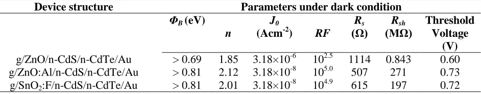
The values of ΦB, J0 and RF obtained from figure 1 for the three different device structures are presented in Table 1 for easy comparison. From the graph of ln 𝐽 vs. V (where ln 𝐽 = 2.303 log 𝐽 𝑎𝑛𝑑 𝐽 = 𝐼 𝐴⁄ , with A as the device active area), the values of the diode ideality factor, n. for the three device structures were obtained using Eq (6). The results are also shown in Table 1. The n-values obtained are 1.85, 2.12 and 2.01 for the g/ZnO/n-CdS/n-CdTe/Au, g/ZnO:Al/n-CdS/n-CdTe/Au and g/SnO2:F/n-CdS/n-CdTe/Au devices, respectively. The n
device. Therefore the actual potential barrier present is greater than the calculated ΦB values
[image:8.612.71.542.156.248.2]from the above equations.
Table 1: Device parameters in dark condition, for the g/TCO/n-CdS/n-CdTe/Au Schottky barrier diodes.
Device structure Parameters under dark condition ΦB(eV)
n
J0
(Acm-2) RF Rs
(Ω) (MΩ) Rsh Threshold Voltage (V) g/ZnO/n-CdS/n-CdTe/Au > 0.69 1.85 3.18×10⁻⁶ 102.5 1114 0.843 0.60 g/ZnO:Al/n-CdS/n-CdTe/Au > 0.81 2.12 3.18×10⁻⁸ 105.0 507 271 0.73
g/SnO2:F/n-CdS/n-CdTe/Au > 0.81 2.01 3.18×10 -8
104.9 615 197 0.72
Figures 2(a), (b) and (c) show the dark linear J-V graphs of g/ZnO/n-CdS/n-CdTe/Au, g/ZnO:Al/n-CdS/n-CdTe/Au and g/SnO2:F/n-CdS/n-CdTe/Au Schottky diodes respectively. As
described earlier, the series resistance, Rs, and shunt resistance, Rsh, of these diodes are obtained from these graphs. These values are also shown in Table 1 for comparison. A close look at the shapes of the forward currents in figure 2 shows that the g/ZnO/n-CdS/n-CdTe/Au diode has higher series resistance compared to the other two device structures. This diode also has the lowest threshold voltage, which is the voltage beyond which a sharp increase in forward current is observed. The respective threshold voltages estimate from figures 2(a), (b) and (c) are also given in Table 1. When the reverse bias currents are zoomed into, the shunt resistances of the three devices were obtained with values of 0.843 MΩ, 271 MΩ and 197 MΩ for the g/ZnO/n-CdS/n-CdTe/Au, g/ZnO:Al/n-CdS/n-CdTe/Au and g/SnO2:F/n-CdS/n-CdTe/Au Schottky diodes
respectively. It is clear that when Rs increases and Rsh decreases, the rectifying quality of the diodes deteriorates. Therefore the TCOs and any other buffer layers should be added to minimize
Rs and maximize Rsh values. The processing steps should also be optimized to minimize
recombination within the device and hence reduce the n values.
To critically and comprehensively analyse the behavior and performance of the three device structures under dark condition, we look closely at the device parameters in Table 1 as well as some of the important parameters of the three different TCOs and CdS as shown in Table 2. From Tables 1 and 2, one observes that the device with ZnO front contact has the lowest values of barrier height, rectification factor, shunt resistance, threshold voltage and conductivity compared to the devices with ZnO:Al and SnO2:F front contacts. These lowest values of device
parameters give a hint to the poor performance of this device as they indicate poor rectification property of the device. They are all related and principally arise from the lowest Schottky barrier height (ΦB). The device is therefore leaky with very low shunt resistance. ZnO also introduces the highest Rs and hence degrades the solar cell performance. For the devices with ZnO:Al and
comparison. From Tables 1 and 2 again, one notices that this same device structure (with ZnO) shows the highest values of reverse saturation current density, series resistance and resistivity.
Table 2: Some reported important parameters of ZnO, ZnO:Al, SnO2:F and CdS material layers.
Material layer
Bandgap, Eg (eV)
Electrical conductivity,
σ (Ωcm)-1
Electrical resistivity, ρ (Ωcm) Work function, ϕ (eV) Electron affinity, χ (eV) ZnO 3.20 - 3.37
[24] 6.13×10⁻² [24] 1.63×101 [24] 4.71 [25] 4.20-4.60 [26] ZnO:Al 3.31 - 3.37
[24]
1.06 – 11.23 [24]
8.90×10⁻² – 9.43×10⁻¹ [24]
4.62 [25,27]
--
SnO2:F 3.80-4.00
[28,29]
3.40×10²-5.7×10³ [29,30]
1.75×10⁻⁴ – 2.94×10⁻³ [29,30]
4.40 – 5.70 [31,32]
--
CdS 2.42 [20]
2.04×10⁻⁵ – 4.76×10⁻⁵ [33]
2.10×10⁴ – 4.90×10⁴ [33]
4.40-5.20 [34]
--
The highest leakage current (J0) value of course arises from the observed lowest barrier height,
lowest rectification factor and lowest shunt resistance all of which leads to current leakage in a diode. The highest series resistance in this device derives partly from the highest reported resistivity (ρ). A close look at the reported work function (ϕ) of these three TCOs and CdS in Table 2, indicates that ZnO and ZnO:Al have particular ϕ values compared to SnO2:F and CdS
with a range of reported values. This suggest that SnO2:F and CdS have more easily adjustable
work function compared to ZnO and ZnO:Al. Again the range of values of work function for SnO2:F and CdS is similar. This also indicates that it is possible to have these two materials with
equal or nearly equal work functions in a device. Considering the importance of work function in the formation of ohmic contacts to semiconductor surfaces, one could obtain a very good ohmic contact between SnO2:F and CdS. This is most likely the case in these device structures under
study if we consider the lowest work function values for SnO2:F and CdS in Table 2. In this case,
these two semiconductors have similar work function of 4.40 eV.
With this, we can then see what happens at the TCO/CdS interface in terms of the nature of electrical contact formed there with the aid of the energy band diagrams shown in figure 3. The difference in work function (Δϕ) between ZnO and CdS then becomes Δϕ ≈ 0.31 eV and with the largest band offset. Between ZnO:Al and CdS we have Δϕ ≈ 0.22 eV, and between SnO2:F and
This contributes to the series resistance of the device with ZnO front contact as seen in Table 1. For the ZnO:Al front contact, Δϕ and the band offset between ZnO:Al and CdS are lower compared to the case of ZnO. As a result the ZnO:Al/CdS interface has a better ohmic contact with low contact resistance resulting in reduced value of Rs in this device as seen in Table 1. The SnO2:F/CdS interface also produces a good ohmic contact with low contact resistance as seen in
Table 1. Thus one observes the two devices involving ZnO:Al and SnO2:F showing very close
device parameters in Table 1. The above situation therefore gives rise to two possible device structures for these three devices in terms of what happens at the TCO/CdS interface. The energy band diagrams of these two possible device structures are shown in figure 3.
Figure 4 shows the current density-voltage graphs of the same three devices under AM1.5 illumination condition. The solar cell device parameters extracted from these graphs are also presented in Table 3 for easy comparison. A look at the J-V graphs in figure 4 immediately shows the lowest Voc and FF values produced by the device involving ZnO. The shape of the graph also indicates the high series resistance characterizing this same device. The reasons for these poor device parameters have already been given earlier based on the lowest “effective” Schottky barrier height, lowest rectification factor and highest resistivity of ZnO in this device. However, the Jsc is highest indicating the existence of low defects in the material of the device. In all, the device involving SnO2:F (i.e. g/SnO2:F/n-CdS/n-CdTe/Au) produces solar cell with the
highest conversion efficiency as shown in Table 3, with Voc = 630 mV, Jsc = 23.5 mAcm-2, FF = 0.44, EFF = 6.5%, Rs = 221 Ω and Rsh = 8136 Ω. The next best solar cell is produced by the
device structure g/ZnO:Al/n-CdS/n-CdTe/Au employing ZnO:Al with efficiency of 6.0%, Voc =
[image:10.612.92.524.484.562.2]610 mV, Jsc = 24.0 mAcm-2, FF = 0.41, Rs = 225 Ω and Rsh = 8843 Ω. The device structure with ZnO produced an efficiency of 4.1%.
Table 3: AM 1.5 device parameters of the g/TCO/n-CdS/n-CdTe/Au Schottky barrier solar cells.
Device structure Parameters under illumination Voc
(mV)
Jsc
(mAcm-2) FF
EFF (%)
Rs
(Ω) (Ω) Rsh g/ZnO/n-CdS/n-CdTe/Au 410 31.5 0.32 4.1 221 5195 g/ZnO:Al/n-CdS/n-CdTe/Au 610 24.0 0.41 6.0 225 8843 g/SnO2:F/n-CdS/n-CdTe/Au 630 23.5 0.44 6.5 221 8136
The highest Jsc value of 31.5 mAcm-2 and corresponding low series resistance of this device with ZnO is worthy of note even though it produced the overall lowest device performance. This high
Jsc value with the corresponding low value of Rs suggests that ZnO is very photoactive (or
photoconductive), such that its resistivity reduces drastically from 1114 Ω to 221 Ω under illumination. However, this gain in Jsc and the associated low Rs could not compensate for the
low Voc, low shunt resistance and low fill factor, all of which arise mainly from low Schottky
device and not just a single device parameter. The observation of very high Jsc values in some
solar cells but with overall low conversion efficiency is a common phenomenon from authors’ experience. It should also be noted that these device structures are not ideal structures and therefore can deviate from normal ideal device behavior.
4.0 Conclusion
Fabrication of three n-n heterojunction+Schottky barrier devices of general structure g/TCO/n-CdS/n-CdTe/Au, using electrodeposited CdS and CdTe thin films and commercially available TCOs has been reported. The three different commercially available TCOs used were ZnO, ZnO:Al and SnO2:F. Assessment of the resulting device structures under dark condition shows
that all three devices show good diode rectification properties. However, the device structure involving ZnO resulted in diode with the lowest Schottky barrier height (ΦB), lowest rectification factor (RF) and lowest threshold voltage. The two devices that involve ZnO:Al and SnO2:F
showed better device performance with closely similar device parameters. Under AM 1.5 illumination condition, the resulting solar cell with SnO2:F produced the best cell efficiency of
6.5% and is followed by the device with ZnO:Al with an efficiency of 6.0%. The device made with ZnO still produced the lowest solar cell efficiency of 4.1%. The poor overall performance of the device structure g/ZnO/n-CdS/n-CdTe/Au compared to g/ZnO:Al/n-CdS/n-CdTe/Au and g/SnO2:F/n-CdS/n-CdTe/Au is attributed to possible formation of undesired weak Schottky
barrier at the ZnO/n-CdS interface (due to the relatively largest work function difference between ZnO and CdS) as well as to the highest reported resistivity of ZnO. These results will provide insight to device developers who employ TCOs either as buffer materials or as electrodes in choosing their desired TCOs for optimum device performance.
Acknowledgement
The principal author would like to thank the Federal University of Technology, Owerri, Nigeria and University of the Free State, South Africa for financial assistance.
Conflict of interest: The authors declare that they have no conflict of interest.
References
[2] T. M. Razykov, C. S. Ferekides, D. Morel, E. Stefanakos, H. S. Ullal and H. M. Upadhyaya, Solar Photovoltaic electricity: Current status and future prospects, Solar Energy 85, 1580 – 1608 (2011).
[3] B. E. McCandless and J. R. Sites, Cadmium telluride solar cells. In Handbook of Photovoltaic Science and Engineering, A. Luque and S. Hegedus (Eds), John Wiley and Sons, Ltd, (2003).
[4] I. M. Dharmadasa, P. A. Bingham, O. K. Echendu, H. I. Salim, T. Druffel, R.
Dharmadasa, G. U. Sumanasekera, R. R. Dharmasena, M. B. Dergacheva, K. A. Mit, K. A. Urazov, L. Bowen, M. Walls and A. Abbas, Fabrication of CdS/CdTe-based thin film solar cells using an electrochemical technique, Coatings 4, 380 – 415 (2014).
[5] D. G. Diso, F. Fauzi, O. K. Echendu, O. I. Olusola and I. M. Dharmadasa, Optimisation of CdTe electrodeposition voltage for development of CdS/CdTe solar cells, Journal of Materials Sciene:Materials in Electronics 27, (12) 12464 – 12472 (2016)..
[6] S. D. Sordo, L. Abbene, E. Caroli, A. M. Mancini, A. Zappettini and P. Ubertini,
Progress in the development of CdTe and CdZnTe semiconductor radiation detectors for Astrophysical and Medical applications, Sensors 9, 3491-3526 (2009).
[7] S.M. Sze, K.K. Ng, Physics of Semiconductor Devices, 3rd ed., John Wiley & Sons, Inc, New Jersey, , p. 154 (2007).
[8] T. Schulmeyer, J. Fritsche, A. Thiβen, A. Klein, W. Jaegermann, M. Campo and J. Beier, Effect of in situ UHV CdCl2-activation on the electronic properties of CdTe thin film
solar cells. Thin Solid Films 431–432, 84–89 (2003).
[9] O. K. Echendu, F. Fauzi, A. R. Weerasinghe and I M. Dharmadasa, High short-circuit current density CdTe solar cells using all-electrodeposited semiconductors. Thin Solid Films 556, 529–534 (2014).
[10] O. K. Echendu and I. M. Dharmadasa, Graded-bandgap solar cells using all- electrodeposited ZnS, CdS and CdTe thin-films, Energies 8, 4416-4435 (2015).
[12] V.Camarchia, F.Cappelluti, G.Ghione, E.Limiti, D. A. J. Moran, M.Pirola, An overview on recent developments in RF and microwave power H-terminated diamond MESFET technology,Integrated Nonlinear Microwave and Millimetre-wave Circuits (INMMiC), IEEE International Workshop, Leuven, Belgium, April (2014).
Doi:10.1109/INMMIC.2014.6815102.
[13] K. J. Chen, A. M. H. Kwan, and Z. Tang, Recent development in flourine-ion-implanted GaN-based heterojunction power devices, Wide Bandgap Power Devices and
Applications (WiPDA), 2013 IEEE Workshop, Columbus, USA, October (2013). Doi:10.1109/WiPDA.2013.6695570.
[14] X. Wu, J. C. Keane, R. G. Dhere, C. Dettart, D. S. Albin, A. Duda, T. A. Gessert, S. Ashar, D. H. Levi and P. Sheldon, 16.5%-efficient CdS/CdTe polycrystalline thin film solar cell, Proceedings of 17th European PVSEC, Munich, Germany, 22 – 26 October (2001) 995 – 1000.
[15] I. M. Dharmadasa, O. K. Echendu, R. Dharmadasa and F. Fauzi, Distortions observed in current-voltage characteristics of photovoltaic solar cells. Proceedings of 27th European
Photovoltaic Solar Energy Conference and Exhibition, Frankfurt, Germany (2012) 2308 – 2313.
[16] A. Rios-Flores, O. Ares, J. M. Camacho, V. Rejon and J. L. Pena, Procedure to obtain higher than 14% efficient thin film CdS/CdTe solar cells activated with HCF2Cl gas. Solar Energy 86, 780–785 (2012).
[17] R. G. Dhere, M. Bonnet-Eymard, E. Charlet, E. Peter, J. N. Duenow, J. V. Li, D.
Kuciauska and T. A. Gessert, CdTe solar cell with industrial Al:ZnO on soda-lime glass. Thin Solid Films 519, 7142–7145 (2011).
[18] N. R. Paudel, K. A. Wieland and A. D. Compan, Ultrathin CdS/CdTe solar cells by sputtering, Sol. Energ. Mat. Sol. Cells 105, 109 – 112 (2012).
[19] P. Panayotatos and H.C. Card, Use of Voc/Jsc measurements for determination of barrier
height under illumination and for fill-factor calculations in Schottky-barrier solar cells, IEE Proceedings, Solid State and Electron Devices 127, (6) 308-311 (1980).
[21] O. K. Echendu, K. B. Okeoma, C. I. Oriaku and I.M. Dharmadasa, Electrochemical deposition of CdTe semiconductor thin films for solar cell application using two- electrode and three-electrode configurations: A comparative study, Adv. in Mater. Sci. Eng 1 – 8 (2016).
[22] O. K. Echendu, F. Fauzi, A. R. Weerasinghe, and I. M. Dharmadasa, High short-circuit current density CdTe solar cells using all-electrodeposited semiconductors, Thin Solid Films 556, 529–534 (2014).
[23] O. K. Echendu and I. M. Dharmadasa, The effect on CdS/CdTe solar cell conversion efficiency of the presence of fluorine in the usual CdCl2 treatment of CdTe, Mater.
Chem. Phys 157, 39 – 44 (2015).
[24] H. H. Lai, T. Basheer, V. L. Kuznetsov, R. G. Egdell, R. M. J. Jacobs, M. Pepper and P. P. Edwards, Dopant-induced bandgap shift in Al-doped ZnO thin films prepared by spray pyrolysis, J. Appl. Phys 112, 083708-1 – 083708-5 (2012).
[25] M. Wei, C. Li, X. Deng and H. Deng, Surface Work Function of Transparent Conductive ZnO Films, Energy Procedia 16, 76 – 80 (2012).
[26] S. A. Chevtchenko,a_ J. C. Moore, Ü. Özgür, X. Gu, A. A. Baski, and H. Morkoç, Comparative study of the (0001) and (0001̅) surfaces of ZnO, Appl. Phys. Lett 89, 182111-1 – 182111-3 (2006).
[27] T. W. Kim, D. C. Choo, Y. S. No, W. K. Choi, E. H. Choi, High work function of Al- doped zinc-oxide thin films as transparent conductive anodes in organic light-emitting devices, Appl. Surf. Sci 253, 1917–1920 (2006).
[28] Z. Y. Banyamin, P. J. Kelly, G. West and J. Boardman, Electrical and optical properties of fluorine-doped tin oxide thin films prepared by Magnetron sputtering, Coatings 4, 732-746 (2014).
[29] P. Karthick, D. Vijayanarayanan, S. Suja, M. Sridharan and K. Jeyadheepan, Opto- electronic properties of fluorine doped tin oxide films deposited by Nebulized spray pyrolysis method, Asian Journal of Applied Sciences 8, (4) 259-268 (2015).
[31] A. Klein, C. Körber, A. Wachau, F. Säuberlich, Y. Gassenbauer, R. Schafranek,
S. P. Harvey and T. O. Mason, Surface potentials of magnetron sputtered transparent conducting oxides, Thin Solid Films 518, 1197–1203 (2009).
[32] M. Batzill and U. Diebold, The surface and materials science of tin oxide, Progress in Surface Science 79, 47–154 (2005).
[33] O. K. Echendu, Thin film solar cells using all-electrodeposited ZnS, CdS and CdTe materials, Ph.D thesis, Sheffield Hallam University, United Kingdom (2014).
[34] K. Sasaki, Study on work function of {0001} faces of CdS crystal. I., Jap. J. Appl. Phy
List of figures
Fig. 1: Dark logI vs. V graphs of (a) g/ZnO/n-CdS/n-CdTe/Au, (b) g/ZnO:Al/n-CdS/n-CdTe/Au and (c) g/SnO2:F/n-CdS/n-CdTe/Au Schottky diodes respectively.
Fig. 2: Dark J-V graphs of g/ZnO/n-CdS/n-CdTe/Au, g/ZnO:Al/n-CdS/n-CdTe/Au and g/SnO2:F/n-CdS/n-CdTe/Au Schottky diodes respectively.
Fig. 3: Proposed energy band diagrams of the TCO/n-CdS/-CdTe/Au Schottky barrier device (a) with low-resistance ohmic contact at the TCO/n-CdS interface and (b) with possible weak Schottky barrier at the TCO/n-CdS interface. The weak Schottky barrier junction is
indicated with a pink circle in figure 3 (b).
Fig. 4:J-V graphs of g/ZnO/n-CdS/n-CdTe/Au, g/ZnO:Al/n-CdS/n-CdTe/Au and g/SnO2:F/n-