warwick.ac.uk/lib-publications Manuscript version: Author’s Accepted Manuscript
The version presented in WRAP is the author’s accepted manuscript and may differ from the published version or Version of Record.
Persistent WRAP URL:
http://wrap.warwick.ac.uk/123458
How to cite:
Please refer to published version for the most recent bibliographic citation information. If a published version is known of, the repository item page linked to above, will contain details on accessing it.
Copyright and reuse:
The Warwick Research Archive Portal (WRAP) makes this work by researchers of the University of Warwick available open access under the following conditions.
Copyright © and all moral rights to the version of the paper presented here belong to the individual author(s) and/or other copyright owners. To the extent reasonable and
practicable the material made available in WRAP has been checked for eligibility before being made available.
Copies of full items can be used for personal research or study, educational, or not-for-profit purposes without prior permission or charge. Provided that the authors, title and full
bibliographic details are credited, a hyperlink and/or URL is given for the original metadata page and the content is not changed in any way.
Publisher’s statement:
Please refer to the repository item page, publisher’s statement section, for further information.
1
Visualizing electrostatic gating effects in two-dimensional heterostructures
1 2
Paul V Nguyen,1 Natalie C Teutsch*,2 Nathan Wilson,1 Joshua Kahn,1 Xue Xia*,2 Abigail J
3
Graham*,2 Viktor Kandyba,3 Alessio Giampietri,3 Alexei Barinov,3 Gabriel C Constantinescu,4 Nelson
4
Yeung,2 Nicholas D M Hine,2 Xiaodong Xu,1,5* David H Cobden,1* Neil R Wilson*2*
5
1Department of Physics, University of Washington, Seattle, Washington 98195, USA
6
2Department of Physics, University of Warwick, Coventry, CV4 7AL, UK
7
3Elettra - Sincrotrone Trieste, S.C.p.A., Basovizza (TS), 34149, Italy
8
4TCM Group, Cavendish Laboratory, University of Cambridge, 19 JJ Thomson Avenue, Cambridge
9
CB3 0HE, UK 10
5Department of Material Science and Engineering, University of Washington, Seattle, Washington
11
98195, USA 12
13
Submitted and accepted to Nature 14
15
The ability to directly monitor the states of electrons in modern field-effect devices, for example 16
imaging local changes in the electrical potential, Fermi level and band structure as a gate voltage is 17
applied, could transform understanding of the device physics and function. Here we show that 18
submicrometre angle-resolved photoemission spectroscopy1–3 (-ARPES) applied to
two-19
dimensional van der Waals heterostructures4 affords this ability. In two-terminal graphene devices
20
we observe a shift of the Fermi level across the Dirac point, with no detectable change in the 21
dispersion, as a gate voltage is applied. In two-dimensional semiconductor devices we see the 22
conduction band edge appear as electrons accumulate, thereby firmly establishing its energy and 23
momentum. In the case of monolayer WSe2 we observe that the band gap is renormalized 24
downwards by several hundred meV, approaching the exciton energy, as the electrostatic doping 25
increases. Both optical spectroscopy and -ARPES can be carried out on a single device, allowing 26
definitive studies of the relationship between gate-controlled electronic and optical properties. The 27
technique provides a powerful new means to study not only fundamental semiconductor physics 28
but also intriguing phenomena such as topological transitions5 and many-body spectral
29
reconstructions under electrical control. 30
31
In ARPES one measures the distribution of energy and momentum of electrons photoemitted from 32
a solid sample subjected to a narrow-spectrum ultraviolet or X-ray excitation. This provides 33
information about the energy and momentum of the initial occupied electron states, and hence the 34
band structure and Fermi level. As electrons are emitted only from very near the sample surface, 35
ARPES is not useful for studying conventional semiconductor devices. On the other hand, it is well 36
suited to probing two-dimensional (2D) materials, and has been applied to films of graphene6,
37
transition metal dichalcogenides (MX2, where M=Mo,W,Ta etc and X=S,Se,Te)7,8, and others9,10. While
38
the excitation spot size is typically measured in millimetres, efforts have been made in the last decade2
39
to perform ARPES with a focused beam suitable for small or nonuniform samples. Micrometre-scale 40
spot sizes (hence µ-ARPES) have been achieved in at least four commissioned synchrotron beamlines 41
using Schwarzschild objectives1, Fresnel zone plates2,3, or capillary mirror optics11. µ-ARPES has
42
allowed the study of atomically thin exfoliated flakes of 2D materials, which are typically tens of 43
microns or less in size12, and of heterostructures4 made by stacking such flakes of different
44
materials13,14, revealing for example band offsets and interlayer hybridization15–17
. Such 2D
45
heterostructures can be made into electrical and optical devices18 by incorporating metal electrodes,
46
opening up the possibility of using -ARPES to monitor electronic structure in operating devices. 47
A major limitation of ARPES is that it probes only occupied electron states. A semiconductor sample 48
must therefore be electron-doped in order to obtain a signal from the conduction band. Doping is 49
usually achieved by depositing electropositive atoms such as alkali metals6–8,13 on the surface. This
2
process cannot be controlled accurately and can only be reversed by high temperature annealing; 1
moreover, it chemically perturbs the electronic structure and introduces disorder through the random 2
distribution of dopants. In this work we demonstrate purely electrostatic doping, which has none of 3
these disadvantages. We thereby obtain momentum-resolved electronic spectra and direct 4
visualization of Fermi level shifts and band structure changes induced by applying a gate voltage. 5
We first demonstrate and validate the technique using graphene, then go on to apply it to the 2D 6
MX2 semiconductors which are of interest for valleytronics and other applications18,19. Although it is
7
widely believed that all monolayer MX2 semiconductors have a direct band gap at the corner of the
8
hexagonal Brillouin zone, 𝐊, the location of the conduction band edge (CBE) is not known with 9
certainty. This is illustrated by the wide range of reported band gap values for monolayer WSe2, from
10
1.4 to 2.2 eV8,20–24. Also unclear is when the local conduction band minimum at the lower-symmetry
11
point 𝐐 comes into play21,25. Using electrostatic doping in -ARPES, we confirm that the CBE is at 𝐊 in
12
all the monolayer semiconductors, MoS2, MoSe2, WS2 and WSe2, and in each case we obtain a measure
13
of the band gap. We also study the layer-number dependence in WSe2, finding that the CBE moves to
14
𝐐 in the bilayer, and measure for the first time the renormalization of the band structure on gating. 15
16
1. Electrostatic doping of graphene 17
18
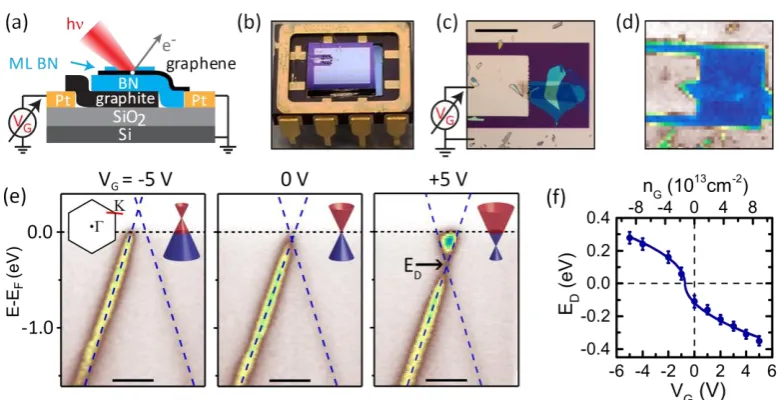
Figure 1. Visualizing electrostatic gating of monolayer graphene. (a) Schematic of a 2D 19
heterostructure device with a stack comprising graphene encapsulated by BN on a graphite back gate.
20
Photoemission is measured with a focused micron-size X-ray beam spot (see Methods). The graphene
21
is grounded while a gate voltage 𝑉𝐺 is applied to the gate. (b) Optical image of a device mounted in a
22
standard dual in-line package. (c) Optical zoom on the dotted box in (b) showing the stack, and (d)
23
scanning photoemission microscopy (SPEM) image of the same area (scale bar, 50 µm). (e)
Energy-24
momentum slices near the graphene K-point, along the red line in the inset Brillouin zone, at the
25
labelled gate voltages. The dashed lines are linear dispersion fits; the Dirac point energy 𝐸𝐷 is deduced
26
from their crossing point (scale bars, 0.2 Å-1). (f) Gate dependence of 𝐸
𝐷, with error bars obtained from
27
the fitting procedure. The solid line is a fit based on the dispersion of graphene, with the gate-induced
28
electron density 𝑛𝐺 shown on the top axis calculated from the capacitance (see Methods).
29 30
We first demonstrate gate-doping of monolayer graphene. A graphene sheet is capped by 31
monolayer hexagonal boron nitride (BN), supported on a BN flake over a graphite gate (Fig. 1a), and 32
located in a gap between two platinum electrodes on an SiO2/Si substrate chip (Figs. 1b and 1c; see
33
Methods). A similar structure with two contacts to the graphene would function as a high-mobility 34
transistor26. Scanning photoemission microscopy (SPEM) is used to locate the sample in the ARPES
35
chamber (Fig. 1d; see Methods). Fig. 1e shows energy, 𝐸 − 𝐸𝐹, vs momentum for a slice through the 36
Dirac cone near the graphene zone corner 𝐊, acquired at a series of gate voltages 𝑉𝐺 at 105 K. As 37
[image:3.595.103.494.304.504.2]3
+5 V. Fitting a linear dispersion, 𝐸(𝒌) = 𝐸𝐷± ħ𝑣𝐹𝑘 (dashed lines), gives 𝐸𝐷 and the Fermi velocity 𝑣𝐹. 1
We find 𝑣𝐹= (9.3 ± 0.1) × 105 ms-1 at 𝑉𝐺= 0 𝑉, with a weak 𝑉𝐺 dependence (see Extended Data). 2
The variation of 𝐸𝐷 with 𝑉𝐺 (Fig. 1f) is consistent with the expected form for this dispersion (solid line, 3
see Methods). No modification of the dispersion near 𝐸𝐷, which could arise due to interactions, is 4
detectable with the current spectral resolution. 5
The consistency of the above properties with the graphene literature, together with the 6
observation that the spectrum is undistorted as 𝑉𝐺 is changed, implies that the photoelectron 7
trajectories are not affected by stray electric fields due to the gate voltage or charging effects. We 8
conclude that the technique produces accurate local electronic spectra during live electrostatic gating. 9
10
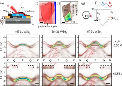
2. Electrostatic population of the conduction band in 2D semiconductors 11
An MX2 flake can be incorporated in the stack on top of the BN, partially overlapping graphene that
12
acts as a contact to it (Fig. 2a). Figures 2b and c are optical and SPEM images of a device with a WSe2
13
flake that has monolayer (1L), bilayer (2L) and trilayer (3L) regions. Figures 2d-f are momentum slices 14
obtained with the beam spot on each of the regions, respectively, along 𝚪 − 𝐊 of the WSe2 Brillouin
15
zone at 100 K (Fig. 2g, inset). As expected, at 𝑉𝐺= 0 (upper row) only the valence bands can be seen. 16
Their evolution with layer number is consistent with the literature27 and matches the overlaid density
17
functional theory (DFT) predictions well (Methods). At 𝑉𝐺= +3.35 V (lower row) an additional spot 18
appears near 𝐸𝐹. The size of this conduction band feature is determined solely by the instrument 19
resolution. In 1L WSe2 the spot is located at 𝐊, whereas in 2L and 3L it is at 𝐐 (see Fig. 2g). This is
20
consistent with evidence from photoluminescence25 that the gap is direct at 𝐊 in the monolayer but
21
indirect for 2+ layers. 22
[image:4.595.85.513.374.674.2]23
Figure 2. Layer-number dependent conduction band edge (CBE) in WSe2. (a) Schematic of a device
24
incorporating a WSe2 flake, with overlapping graphene top contact grounded and gate voltage 𝑉𝐺
25
applied to the graphite back gate. (b) Optical and (c) SPEM images of WSe2 Device 1 (𝑑𝐵𝑁 = 7.4 ± 0.5
26
nm), with monolayer, bilayer and trilayer regions identified (scale bars, 5 µm). (d)-(f)
Energy-27
momentum slices along 𝚪 − 𝐊 for 1L, 2L, and 3L regions respectively. The upper panels are at 𝑉𝐺 = 0
28
and the lower ones at 𝑉𝐺= +3.35 𝑉. The intensity in the dashed boxes is multiplied by 20. The fuzzy
29
spots signal population of the CBE. Scale bars, 0.3 Å-1. The data have been reflected about 𝚪 to aid
4
comparison with DFT predictions (red dashed lines). (g) Brillouin zone of MX2,and schematic of bands
1
along 𝚪 − 𝐊 showing definitions of the energy parameters discussed in the text.
[image:5.595.72.503.193.305.2]2
Table 1 displays the band parameters for 1L–3L WSe2 as well as for other monolayer MX2 species,
3
derived15 from measurements on this and other devices (see SI section S5). The band gap, 𝐸
𝑔= 𝐸𝐶− 4
𝐸𝐾, where 𝐸𝐶 is the energy of the CBE, was determined at a doping level of 𝑛𝐺≈ 1013 cm-2 for which 5
𝐸𝐹− 𝐸𝐶 ~ 30 meV (see Methods). We also list the simultaneously determined hole effective mass 6
𝑚𝐾∗, valence band edge 𝐸𝐾, spin-orbit splitting ∆𝑆𝑂𝐶, and 𝐸𝐾Γ as defined in Fig. 2g, all measured for 7
the first time on an hBN substrate with no cap and with greater precision than in previous reports. 8
9
∆𝑆𝑂𝐶
(eV) 𝐸𝐾 ((eV)𝑉𝐺= 0) 𝐸𝐾Г ((eV)𝑉𝐺 = 0) 𝑚𝐾
∗/𝑚
𝑒 𝐸𝑔
(eV)
1L MoS2 0.17 ± 0.04 1.93 ± 0.02 0.14 ± 0.04 0.7 ± 0.1 2.07 ± 0.05
1L MoSe2 0.22 ± 0.03 1.04 ± 0.02 0.48 ± 0.03 0.5 ± 0.1 1.64 ± 0.05
1L WS2 0.45 ± 0.03 1.43 ± 0.02 0.39 ± 0.02 0.5 ± 0.1 2.03 ± 0.05
1L WSe2 0.485 ± 0.010 0.80 ± 0.01 0.62 ± 0.01 0.42 ± 0.05 1.79 ± 0.03
2L WSe2 0.501 ± 0.010 0.75 ± 0.01 0.14 ± 0.01 0.41 ± 0.05 1.51 ± 0.03 *
3L WSe2 0.504 ± 0.010 0.74 ± 0.01 0.00 ± 0.01 0.40 ± 0.05 1.46 ± 0.03 *
*indirect, with CBE at 𝑸
[image:5.595.149.448.410.614.2]10 11
Table 1. Measured band structure parameters of MX2 semiconductors. As defined in Fig. 2g, ∆𝑆𝑂𝐶 is the
spin-12
orbit splitting of the valence band at 𝐊; 𝐸K is the valence band edge at 𝑉𝐺= 0; 𝐸𝐾Г= 𝐸𝐾− 𝐸Γ is the difference
13
between the valence band edges at 𝐊 and 𝚪 at 𝑉𝐺= 0; 𝑚𝐾∗ is the effective mass of the valence band edge at 𝐊
14
in units of the free electron mass 𝑚𝑒; and 𝐸𝑔 is the band gap measured at gate-induced electron density 𝑛𝐺=
15
1.0 ± 0.2 × 1012 cm-2. The stage temperature was 100 K for the WSe
2 and 105 K for the others.
16 17
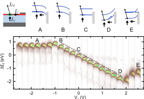
3. Gate dependence of the electronic structure of a semiconducting monolayer 18
19
Figure 3. Electrostatic gating of monolayer WSe2. Each vertical strip is an energy-momentum slice, 0.6
20
Å-1wide, through 𝚪 in WSe
2 Device 2 (𝑑ℎ𝐵𝑁 = 6.0 ± 0.5 nm) measured at the gate voltage shown on
21
the bottom axis. Δ𝐸Γ is the photoelectron kinetic energy measured relative to the Γ-point maximum at
22
𝑉𝐺= 0. The dashed line has slope −1/𝑒. Above left is a device schematic indicating the photoemission
23
current 𝐼𝑃𝐸 from the beam spot, current 𝐼𝐶 from the graphene contact, and current 𝐼𝐺 from the gate
24
through the BN due to photoconductivity. The schematic band diagrams indicate the situations at the
25
gate voltages labelled A-E. The gray rectangle is the graphene Fermi sea, the blue lines are the WSe2
26
conduction and valence band edges, and the smaller arrows indicate when 𝐼𝐺 and 𝐼𝐶 are significant.
27 28
We now investigate the full gate dependence of -ARPES spectra. Figure 3 shows the behavior of 29
the top of the valence band at 𝚪, where the photoemission signal is strongest, for monolayer WSe2
5
Device 2. At low 𝑉𝐺 (range labelled B-C-D) the spectrum shifts nearly linearly with a slope −1/𝑒, where 1
𝑒 is the electron charge, implying that the electrostatic potential in the WSe2 tracks the gate potential
2
when it is undoped. For 𝑉𝐺 > +2.1 V (E) or < -1.5 V (A) it becomes almost independent of 𝑉𝐺, implying 3
that these are the thresholds for electron and hole accumulation, respectively. The behavior can be 4
understood in more detail with reference to the corresponding band diagrams shown above, taking 5
into account the balance of the current of photoemitted electrons, 𝐼𝑃𝐸, the currents into the beam 6
spot from the contact, 𝐼𝐶, and the gate, 𝐼𝐺, as indicated in the sketch at the top left (see Methods). 7
Note that no change in spectral widths is seen as long as the WSe2 is insulating (range B-D in Fig.
8
3), but above threshold (range D-E) all features are smeared in energy by a similar amount. This can 9
be explained by inhomogeneous broadening due to variation of the potential across the beam spot 10
associated with lateral current flow in the WSe2. Refinement of the technique to reduce this effect
11
may allow studies of changes in intrinsic broadening with doping. 12
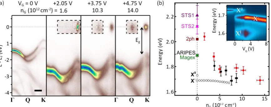
13
Figure 4. Renormalization of the band gap and comparison with optical spectroscopy. (a) Energy-14
momentum slices along 𝚪-𝐊 for monolayer WSe2 in Device 1 at a series of 𝑉𝐺, with doping 𝑛𝐺 also
15
shown (scale bar, 0.3 Å-1). The intensity in the dashed box is multiplied by 20 at +2.05 V and by 40 at
16
higher 𝑉𝐺. The definition of the band gap, 𝐸𝑔, is indicated. (b) Band gap dependence on 𝑛𝐺 for Device
17
1 (red) and also Device 3 (𝑑𝐵𝑁= 24.5 ± 0.5 nm, solid black circles) at 100 K. Also plotted (black open
18
circles) are the photoluminescence peak positions for the neutral exciton (𝑋0) and negative trion (𝑋−)
19
in Device 3 at the same temperature. The inset shows the photoluminescence data, with an
impurity-20
bound exciton peak XI also labelled. The points plotted at 𝑛
𝐺= 0 are measurements of the band gap
21
from other techniques taken from the literature: STS120 (purple triangle) and STS221 (pink triangle) are
22
from scanning tunnelling spectroscopy measurements, on graphite at T= 4.5 K and 77 K respectively;
23
2ph (brown square) is from two-photon absorption22, on SiO
2 at 300 K; ARIPES (black open square) is
24
from inverse photoemission23, on sapphire at 300 K; and Magex (green solid square) is from
magneto-25
optical measurements24, encapsulated in BN at 4 K.
26 27
Figure 4a shows spectra from monolayer WSe2 Device 1 at 𝑉𝐺= 0 (for reference) and at selected
28
gate voltages well above threshold (about +1.5 V). In this regime we derive the gate doping 𝑛𝐺, also 29
shown, from the gate capacitance and threshold voltage (see Methods). The CBE becomes visible at 30
𝐊 for 𝑛𝐺> ~1012 cm-2 and at 𝐐 for 𝑛𝐺> ~1013 cm-2, when 𝐸𝐾 is roughly 30 meV below 𝐸𝐹. We 31
conclude that the conduction band minimum at 𝐐 is higher than that at 𝐊. Scanning tunnelling 32
spectroscopy21 also indicates that for 1L WSe
2 these minima are very close. The form of the valence
33
bands does not change discernibly with increasing 𝑛𝐺, but they shift upwards in energy while the CBE 34
is pinned at 𝐸𝐹, implying that the band gap decreases. 35
Optical spectroscopy can be performed on the same devices, and under the same conditions, as 36
the ARPES measurements, eliminating uncertainties due to differences in sample quality, dielectric 37
environment, gate voltage and temperature28–30. Figure 4b shows both the -ARPES determination of
38
𝐸𝑔 (black solid circles) and the photoluminescence peak positions (black empty circles), 𝐸𝑋0 and 𝐸𝑋−,
[image:6.595.86.520.244.415.2]6 for neutral (X0) and charged (X-) excitons, for monolayer WSe
2 Device 3 as a function of gate doping at
1
100 K. Also shown are the values of 𝐸𝑔 from Device 1 (red solid circles), which agree to within the 2
uncertainty. It is apparent that 𝐸𝑔 decreases systematically, by ~400 meV, as 𝑛𝐺 rises to 1.5 × 10¹³ 3
cm-2. Such renormalization of the band gap with static doping is expected to occur in a semiconductor
4
as a result of free-carrier screening31, though it is has not previously been so accessible to experiments.
5
Also plotted in Fig. 4b are values of the band gap at 𝑛𝐺= 0 inferred from several other techniques. 6
An extrapolation of 𝐸𝑔 measured by -ARPES to 𝑛𝐺= 0 is consistent with scanning tunneling 7
spectroscopy (STS) measurements which put it in the range 2.1-2.2 eV. Comparison with 𝐸𝑋0 supports
8
arguments that the binding energy of neutral excitons in this material is very large28, at several
9
hundred meV. 𝐸𝑔 decreases much faster than 𝐸𝑋− with doping, implying dramatic weakening of the 10
exciton binding which is another expected effect of free-carrier screening29. Finally, the still smaller
11
values of 𝐸𝑔 reported in monolayers doped with alkali metals (down to 1.4 eV for 1L WSe2) are
12
consistent with an extrapolation the renormalization process to higher 𝑛𝐺7,8. 13
The ability to measure changes in the electronic bands in 2D field-effect devices opens up many 14
interesting possibilities. For example, it could be used to study electric-field tuning of the bands across 15
topological phase transitions5; to investigate the doping dependence of spectra in correlated electron
16
systems such as in superconductors, Mott insulators, and charge-density-wave materials; to observe 17
spectral reconstructions in structures with moiré superlattice modulations32; and, with the addition of
18
circularly polarized light or a spin-resolved spectrometer, to study electrically controlled magnetic 19
phenomena33.
20 21
References 22
1. Dudin, P. et al. Angle-resolved photoemission spectroscopy and imaging with a submicrometre 23
probe at the SPECTROMICROSCOPY-3.2L beamline of Elettra. J. Synchrotron Radiat. 17, 445– 24
450 (2010). 25
2. Rotenberg, E. & Bostwick, A. microARPES and nanoARPES at diffraction-limited light sources: 26
opportunities and performance gains. J. Synchrotron Radiat. 21, 1048–1056 (2014). 27
3. Iwasawa, H. et al. Buried double CuO chains in YBa2Cu4O8 uncovered by nano-ARPES. J. Phys.
28
Condens. Matter 4, 9015–9022 (2019).
29
4. Novoselov, K. S., Mishchenko, A., Carvalho, A. & Castro Neto, A. H. 2D materials and van der 30
Waals heterostructures. Science. 353, aac9439 (2016). 31
5. Tong, Q. et al. Topological mosaics in moiré superlattices of van der Waals heterobilayers. Nat. 32
Phys. 13, 356–362 (2017).
33
6. Bostwick, A., Ohta, T., Seyller, T., Horn, K. & Rotenberg, E. Quasiparticle dynamics in graphene. 34
Nat. Phys. 3, 36–40 (2007).
35
7. Riley, J. M. et al. Negative electronic compressibility and tunable spin splitting in WSe2. Nat.
36
Nanotechnol. 10, 1043–1047 (2015).
37
8. Zhang, Y. et al. Electronic Structure, Surface Doping, and Optical Response in Epitaxial WSe2
38
Thin Films. Nano Lett. 16, 2485–2491 (2016). 39
9. Kim, J. et al. Observation of tunable band gap and anisotropic Dirac semimetal state in black 40
phosphorus. Science. 349, 723–726 (2015). 41
10. Tang, S. et al. Quantum spin Hall state in monolayer 1T’-WTe2. Nat. Phys. 13, 683–687 (2017).
42
11. Koch, R. J. et al. Nano focusing of soft X-rays by a new capillary mirror optic. Synchrotron Radiat. 43
News 31, 50–52 (2018).
44
12. Zhang, H. et al. Resolving Deep Quantum-Well States in Atomically Thin 2H-MoTe2 Flakes by
45
Nanospot Angle-Resolved Photoemission Spectroscopy. Nano Lett. 18, 4664–4668 (2018). 46
13. Katoch, J. et al. Giant spin-splitting and gap renormalization driven by trions in single-layer 47
WS2/h-BN heterostructures. Nat. Phys. 14, 355–359 (2018).
48
14. Cucchi, I. et al. Microfocus Laser–Angle-Resolved Photoemission on Encapsulated Mono-, Bi-, 49
and Few-Layer 1T′-WTe2. Nano Lett. 19, 554–560 (2019).
50
7
semiconductor heterostructures. Sci. Adv. 3, e1601832 (2017). 1
16. Jin, W. et al. Tuning the electronic structure of monolayer graphene/ MoS2 van der Waals
2
heterostructures via interlayer twist. Phys. Rev. B 92, 201409 (2015). 3
17. Pierucci, D. et al. Band Alignment and Minigaps in Monolayer MoS2 -Graphene van der Waals
4
Heterostructures. Nano Lett. 16, 4054–4061 (2016). 5
18. Liu, Y. et al. Van der Waals heterostructures and devices. Nature Reviews Materials 1, 16042 6
(2016). 7
19. Schaibley, J. R. et al. Valleytronics in 2D materials. Nat. Rev. Mater. 1, 16055 (2016). 8
20. Yankowitz, M., McKenzie, D. & LeRoy, B. J. Local Spectroscopic Characterization of Spin and 9
Layer Polarization in WSe2. Phys. Rev. Lett. 115, 136803 (2015).
10
21. Zhang, C. et al. Probing Critical Point Energies of Transition Metal Dichalcogenides: Surprising 11
Indirect Gap of Single Layer WSe2. Nano Lett. 15, 6494–6500 (2015).
12
22. He, K. et al. Tightly Bound Excitons in Monolayer WSe2. Phys. Rev. Lett. 113, 026803 (2014).
13
23. Park, S. et al. Direct determination of monolayer MoS2 and WSe2 exciton binding energies on
14
insulating and metallic substrates. 2D Mater. 5, 025003 (2018). 15
24. Stier, A. V. et al. Magnetooptics of exciton Rydberg states in a monolayer semiconductor. Phys. 16
Rev. Lett. 120, 057405 (2018).
17
25. Zhao, W., Ribeiro, R. M. & Eda, G. Electronic Structure and Optical Signatures of 18
Semiconducting Transition Metal Dichalcogenide Nanosheets. Acc. Chem. Res. 48, 91–99 19
(2015). 20
26. Mayorov, A. S. et al. Micrometer-Scale Ballistic Transport in Encapsulated Graphene at Room 21
Temperature. Nano Lett. 11, 2396–2399 (2011). 22
27. Liu, G., Xiao, D., Yao, Y., Xu, X. & Yao, W. Electronic structures and theoretical modelling of two-23
dimensional group-VIB transition metal dichalcogenides. Chem. Soc. Rev. 44, 2643–2663 24
(2015). 25
28. Ugeda, M. M. et al. Giant bandgap renormalization and excitonic effects in a monolayer 26
transition metal dichalcogenide semiconductor. Nat. Mater. 13, 1091–1095 (2014). 27
29. Gao, S., Liang, Y., Spataru, C. D. & Yang, L. Dynamical Excitonic Effects in Doped Two-28
Dimensional Semiconductors. Nano Lett. 16, 5568–5573 (2016). 29
30. Raja, A. et al. Coulomb engineering of the bandgap and excitons in two-dimensional materials. 30
Nat. Commun. 8, 15251 (2017).
31
31. Gao, S. & Yang, L. Renormalization of the quasiparticle band gap in doped two-dimensional 32
materials from many-body calculations. Phys. Rev. B 96, 155410 (2017). 33
32. Cao, Y. et al. Magic-angle graphene superlattices: a new platform for unconventional 34
superconductivity. Nature 556, 43–50 (2018). 35
33. Wang, H., Fan, F., Zhu, S. & Wu, H. Doping enhanced ferromagnetism and induced half-36
metallicity in CrI3 monolayer. EPL 114, 47001 (2016).
37 38
Acknowledgements. 39
The Engineering and Physical Sciences Research Council is acknowledged for support through 40
EP/P01139X/1 and a studentship for NCT (EP/M508184/1). XXia was supported by a University of 41
Warwick studentship. DHC and PVN were supported by US Department of Energy, Office of Basic 42
Energy Sciences, Division of Materials Sciences and Engineering, award DE-SC0002197 and the Pro-43
QM Energy Frontiers Research Center. PVN and JK were also supported in part by NSF MRSEC award 44
1719797. XXu and NPW are supported by Department of Energy, Basic Energy Sciences, Materials 45
Sciences and Engineering Division (DE-SC0018171). NDMH and GCC acknowledge the support of the 46
Winton Programme for the Physics of Sustainability. Computing resources were provided by the 47
Darwin Supercomputer of the University of Cambridge High Performance Computing Service. GCC 48
acknowledges the support of the Cambridge Trust European Scholarship. 49
8 Author contributions.
1
NRW, XXu and DHC conceived and supervised the project. PVN, JK and NW fabricated the samples. 2
NCT, NRW, PVN, XXia, AJG, VK, AG and AB collected ARPES data. NCT, NRW and PVN analyzed µ-3
ARPES data, with input from AB. NPW acquired photoluminescence data. NDMH, NY and GCC 4
performed the band structure calculations. DHC, NRW, PVN and XXu wrote the paper with input from 5
all authors. 6
7
Competing interests. 8
The authors declare no competing interests. 9
10
Materials & Correspondence. 11
Correspondence to [email protected], [email protected], [email protected] 12
13
Methods 14
Sample fabrication. Standard micro-mechanical exfoliation and dry transfer34 with polycarbonate
15
film-based stamping were used. The smaller electrode contacts the graphite gate, as indicated in the 16
optical micrograph in Fig. 1c. The larger electrode, which contacts the graphene, is grounded and 17
covers most of the chip to minimize electrostatic distortion of the photoelectron spectrum when 18
applying a gate voltage. The sample substrates are mounted in dual-inline packages using ultra-high 19
vacuum and high-temperature compatible silver epoxy and wire-bonded. Bare wire is wrapped around 20
the package pins, fixed using the epoxy, and used to contact to leads on the ARPES sample mount. 21
Angle resolved photoemission. Measurements were made at the Spectromicroscopy beamline of 22
the Elettra light source1. Linearly polarized light, at 45° to the sample, was focused to a ~0.6 µm
23
diameter spot by a Schwarzschild objective. The photon energy was 27 eV except for the data in Fig. 24
1 where it was 74 eV. The hemispherical analyser with two-dimensional detector on a two-axis 25
goniometer permitted a resolution of approximately 50 meV and 0.03 Å-1. After mounting in the
26
chamber on a scanning stage with 100 nm closed loop positioning accuracy, the samples were located 27
by scanning photoemission microscopy (SPEM). With the light focus fixed, the photoelectron intensity 28
on the detector was acquired point by point as the sample was stepped relative to the light spot. In 29
the SPEM images the colour corresponds to the integrated photoelectron intensity around 𝚪 (over the 30
full detector range of ~15°, corresponding to ~0.6 Å-1 at 20 eV and ~1.1 Å-1 at 70 eV, and binding
31
energy range of 0 to 2.5 eV in Fig. 1d and 0 to 3.5 eV in Fig. 2c) at that point on the sample. For spectral 32
acquisition, the entrance slit to the analyser is in a fixed orientation, but its angular coordinates 33
relative to the sample normal are controlled by the two-axis goniometer. For energy-momentum slices 34
along 𝚪 − 𝐊, as in Figs. 2 and 3, a sequence of 2D slices was acquired with the goniometer moving the 35
centre of the analyser entrance slit along the line in reciprocal space from 𝚪 − 𝐊, mapping out a small 36
volume in (E,kx,ky) from which the 𝚪 − 𝐊 slice was later extracted. Over the few hours required to
37
acquire this data, the sample drift was typically < 1 µm. Prior to measurement, samples were annealed 38
in ultrahigh vacuum at 650 K for several hours. The stage temperature was ~100 K (Figs. 2,3 and 4) or 39
~105 K (Fig. 1 and MoS2, WS2 and MoSe2). Following standard practice, we plot 𝐸 − 𝐸𝐹, the negative
40
of the electron binding energy, where 𝐸 is the measured photoelectron kinetic energy and 𝐸𝐹 is the 41
kinetic energy of electrons removed from the Fermi level, determined by fitting the Fermi-Dirac 42
distribution to the drop in photoemitted intensity across the photoemission threshold. 43
Detailed considerations of gate dependence and device operation. The devices have a thin hBN
44
dielectric separating the graphite back-gate electrode from the upper 2D material (2DM) layer, which 45
is either graphene itself or overlaps a graphene contact that in turn overlaps a metal (ground) 46
electrode. When the 2DM is conducting this constitutes a parallel-plate capacitor with geometric areal 47
capacitance 𝐶𝑔 = 𝜀0𝜀𝐵𝑁⁄𝑑𝐵𝑁 , where 𝜀0 is the relative permittivity of free space, 𝜀𝐵𝑁 = 4.0 ± 0.2 is 48
the out-of-plane (c direction) dielectric constant for hBN, and 𝑑𝐵𝑁 is the thickness of the hBN. During 49
photoemission, the electrochemical potential at the emission spot will differ from ground, by an 50
amount Δ𝑉, associated with current flow both to the contact and to the gate which is at voltage 𝑉𝑔,
9
thus reducing the effective gate voltage determining the local carrier density to 𝑉𝑔− Δ𝑉. Δ𝑉 will not
1
exceed the product of the effective electrical resistance 𝑅 between the spot and ground electrode 2
and the maximum current, which is no more than ~2 nA. 3
For graphene devices, the band dispersion is not affected by doping to within 10% accuracy (see 4
Extended Data Fig. 4). In this case we expect 𝑛𝐺 = 𝐶𝑔(𝑉𝐺− ∆𝑉 − ∆𝜇/𝑒), where Δ𝜇 = Δ(𝐸𝐹− 𝐸𝐷) is
5
the chemical potential change due to gate doping (note that 𝐶𝑔 is only the geometric capacitance, and
6
the total capacitance is nonlinear in 𝑉𝐺). For graphene, 𝑅 < ~1 kΩ and thus Δ𝑉 < ~2 µV, which is
7
negligible. Δ𝜇 can be found from the ARPES spectrum at each gate voltage to an accuracy of ~20 meV. 8
In the measurements shown in Fig. 1, Δ𝜇/e is at least ten times smaller than 𝑉𝐺, and thus simply taking
9
𝑛𝐺≈ 𝐶𝑔𝑉𝐺, the quantity plotted on the top axis of Fig. 1f, is accurate to < 10%. When 𝑘𝐵𝑇 ≪ 𝐸𝐷 (valid 10
here since 𝑘𝐵𝑇 = 9 meV), from the conical Dirac dispersion one expects35𝐸𝐷2 ≈ 𝜋ℏ2𝑣𝐹2(𝑛0+ 𝑛𝐺), 11
where 𝑛𝐺 = 𝐶𝑉𝐺 is the gate-induced 2D electron density, 𝐶 the areal capacitance, and 𝑛0 the residual 12
electron density at 𝑉𝐺= 0. The solid line in Fig. 1f is a fit to this model with 𝐶 and 𝑛0 treated as fitting 13
parameters. The value of 𝑛0 obtained is (1.8 ± 0.1) × 1012 cm-2, implying a somewhat high residual 14
doping that may be due to contamination. The value of 𝐶 is (2.2 ± 0.2) × 10−7 Farad cm-2, consistent
15
with the geometrical capacitance, 𝜖0𝜖𝐵𝑁
𝑑𝐵𝑁 = (2.5 ± 0.2) × 10
−7 Farad cm-2, derived from the BN
16
thickness, 𝑑𝐵𝑁 = 14 ± 1 nm, measured by atomic force microscopy, and the dielectric constant, 17
𝜖𝐵𝑁= 4.0, taken from the literature36–38. Note also that the intensity near 𝐸𝐷 is weak because these 18
𝐸 − 𝑘 slices do not pass exactly through 𝐊. The much lower intensity on one side of the cone results 19
from destructive interference between the two carbon sublattices39.
20
For MX2 semiconductor devices the situation is more complicated. At small 𝑉𝐺, the doping 𝑛𝐺 must
21
be very small because of the band gap, so the in-plane resistance can be large and Δ𝑉 can be 22
substantial. As long as 𝑛𝐺 is negligible the bands will not be renormalized and Δ𝑉 can be identified
23
with the purely electrostatic energy shift of an ARPES spectral feature. Δ𝐸Γ/𝑒 in Fig. 3 indeed tracks
24
𝑉𝐺 closely at low 𝑉𝐺 (see Extended Data Fig. 6). We deduce that in this regime photoemission directly
25
from the hBN valence band generates conductivity in the hBN which is sufficient to keep the potential 26
in the MX2 close to that of the gate, i.e., Δ𝑉 ≈ 𝑉𝑔, with negligible potential drop across the hBN and
27
no accumulation of charge in the MX2. In contrast, at a sufficiently large magnitude of 𝑉𝐺,
28
(𝑉𝐺− ∆𝐸Γ/𝑒) tends towards a linear increase with 𝑉𝐺. This happens when the high doping makes
in-29
plane resistance 𝑅 small enough that the electrochemical potential in the MX2 approaches that in the
30
(ground) electrode and Δ𝑉 stops changing, with the Fermi energy virtually pinned at the band edge 31
due to the large density of states. In this regime we can take 𝑛𝐺= 𝐶𝑔(𝑉𝐺− Δ𝐸Γ/𝑒), since 𝑉𝐺− Δ𝐸Γ/𝑒
32
is the static potential drop across the hBN, the electrons are in electrochemical equilibrium, and the 33
quantum capacitance is negligible (i.e., 𝐸𝐹 is effectively pinned at the CBE). The values of 𝑛𝐺 shown in
34
Fig. 4 are obtained in this way. 35
Our interpretation of the behavior in Fig. 3 for monolayer WSe2 is as follows. The photoemission
36
current 𝐼𝑃𝐸, current to the contact, 𝐼𝐶, and to the gate, 𝐼𝐺, indicated in the sketch at the top left of Fig. 37
3, must sum to zero. 𝐼𝐺 can be substantial because of photo-excited carriers in the BN. (It should be 38
borne in mind that in general such currents may cause a device to operate differently from how it 39
would in the dark). Between B and C, the WSe2 is depleted and insulating enough that the BN
40
photoconductivity brings the potential close to that of the gate. Holes created by photoemission from 41
the WSe2 recombine with excited electrons in the BN, and 𝐼𝑃𝐸 ≈ 𝐼𝐺. Between C and D, these holes can 42
also drift to the contact through the depleted WSe2, and 𝐼𝐶 is significant. Above threshold, at E, 43
electrons accumulate at the CBE in the WSe2 as they flow in laterally from the graphene contact, and
44
the CBE is pinned close to the graphene Fermi level. Similarly, at A, holes accumulate and the valence 45
band edge is pinned. An “overshoot” occurs at D because when the CBE in the beam spot first moves 46
below the graphene Fermi level, the Schottky barrier between graphene and WSe2 prevents electrons
47
flowing in fast enough to accumulate. 48
Estimating the CBE energy. The structure of the conduction band is not resolvable in the ARPES 49
data (Fig. 2d-f). The density of states at a single parabolic band edge is 𝑔2𝐷= 𝑔𝑠𝑔𝑣𝑚∗/ℏ2, with spin 50
and valley degeneracies 𝑔𝑠 and 𝑔𝑣 and effective mass 𝑚∗. For 1L WSe2 the conduction band edges are
10
at the K-points, so 𝑔𝑣 = 2, and the band is spin-split by ≈ 40 meV40, hence 𝑔𝑠 = 1 for moderate 1
doping. Calculations40 give 𝑚∗≈ 0.3𝑚𝑒. Using 𝑛
𝐺 = ∫ 𝐹(𝐸)𝑔2𝐷 ∞
𝐸𝑐 𝑑𝐸, where 𝐹(𝐸) is the Fermi-Dirac
2
distribution, then gives 𝐸𝐹− 𝐸𝐶 ≈ 30 meV at 𝑛𝐺 = 1.0 × 1013 cm-2. 3
Optical spectroscopy. Photoluminescence measurements were performed using ~20 µW linearly 4
polarized 532 nm continuous-wave laser excitation in reflection geometry, with the signal collected 5
by a spectrometer and a silicon charge-coupled device, in vacuum in a closed-cycle cryostat. 6
Electronic structure calculations including spin-orbit interaction were made using the Quantum 7
Espresso DFT package41. Structures were first optimized until forces were smaller than 10−4 Ry / Bohr.
8
Geometry optimisations and band structure calculations were performed with an 18×18 in-plane k-9
point grid with 140 Ry plane-wave energy cut off. To avoid interaction between periodic images, the 10
vacuum spacing was 25.0 Å. We used norm-conserving fully relativistic pseudopotentials42 from
11
PseudoDojo43, where the semi-core 4d, 5s and 5p states for W are retained as valence electrons. This
12
results in a lattice constant of 3.32 Å for all three structures. We used the results from calculations 13
with the PBE functional as a starting point for G0W0 calculations which utilised the Yambo code44, with
14
the Godby–Needs plasmon pole approximation45. We used 300 bands, 500 bands and 700 bands for
15
the mono-layer, bilayer and trilayer WSe2, respectively, for the self-energy and dynamical dielectric
16
screening. In order to treat the divergence of the Coulomb interaction during the self-energy 17
calculation, the random integration method46 was used, with 3 × 10⁶ random q-points and 100 random
18
G vectors. 19
Data availability. All data presented in this paper are available at [to be finalised on acceptance]. 20
Additional data related to this paper may be requested from the authors. 21
22
34. Zomer, P. J., Guimarães, M. H. D., Brant, J. C., Tombros, N. & Van Wees, B. J. Fast pick up 23
technique for high quality heterostructures of bilayer graphene and hexagonal boron nitride. 24
Appl. Phys. Lett. 105, 013101 (2014).
25
35. Fang, T., Konar, A., Xing, H. & Jena, D. Carrier statistics and quantum capacitance of graphene 26
sheets and ribbons. Appl. Phys. Lett. 91, 092109 (2007). 27
36. Yu, G. L. et al. Interaction phenomena in graphene seen through quantum capacitance. Proc. 28
Natl. Acad. Sci. 110, 3282–3286 (2013).
29
37. Dean, C. R. et al. Boron nitride substrates for high-quality graphene electronics. Nat. 30
Nanotechnol. 5, 722–726 (2010).
31
38. Kim, K. K. et al. Synthesis and Characterization of Hexagonal Boron Nitride Film as a Dielectric 32
Layer for Graphene Devices. ACS Nano 6, 8583–8590 (2012). 33
39. Mucha-Kruczyński, M. et al. Characterization of graphene through anisotropy of constant-34
energy maps in angle-resolved photoemission. Phys. Rev. B 77, 195403 (2008). 35
40. Kormányos, A. et al. k · p theory for two-dimensional transition metal dichalcogenide 36
semiconductors. 2D Mater. 2, 022001 (2015). 37
41. Giannozzi, P. et al. QUANTUM ESPRESSO: a modular and open-source software project for 38
quantum simulations of materials. J. Phys. Condens. Matter 21, 395502 (2009). 39
42. Hamann, D. R. Optimized norm-conserving Vanderbilt pseudopotentials. Phys. Rev. B - 40
Condens. Matter Mater. Phys. 88, 085117 (2013).
41
43. van Setten, M. J. et al. The PSEUDODOJO: Training and grading a 85 element optimized norm-42
conserving pseudopotential table. Comput. Phys. Commun. 226, 39–54 (2018). 43
44. Marini, A., Hogan, C., Grüning, M. & Varsano, D. yambo: An ab initio tool for excited state 44
calculations. Comput. Phys. Commun. 180, 1392–1403 (2009). 45
45. Godby, R. W. & Needs, R. J. Metal-insulator transition in Kohn-Sham theory and quasiparticle 46
theory. Phys. Rev. Lett. 62, 1169–1172 (1989). 47
46. Castro, A., Räsänen, E. & Rozzi, C. A. Exact Coulomb cutoff technique for supercell calculations 48