warwick.ac.uk/lib-publications
Original citation:
Pham, Thinh H., Fahmy, Suhaib A. and McLoughlin, Ian V.. (2017) An end-to-end
multi-standard OFDM transceiver architecture using FPGA partial reconfiguration. IEEE Access, 5 .
pp. 21002-21015.
Permanent WRAP URL:
http://wrap.warwick.ac.uk/93461
Copyright and reuse:
The Warwick Research Archive Portal (WRAP) makes this work by researchers of the
University of Warwick available open access under the following conditions. Copyright ©
and all moral rights to the version of the paper presented here belong to the individual
author(s) and/or other copyright owners. To the extent reasonable and practicable the
material made available in WRAP has been checked for eligibility before being made
available.
Copies of full items can be used for personal research or study, educational, or not-for-profit
purposes without prior permission or charge. Provided that the authors, title and full
bibliographic details are credited, a hyperlink and/or URL is given for the original metadata
page and the content is not changed in any way.
Publisher’s statement:
“© 2017 IEEE. Personal use of this material is permitted. Permission from IEEE must be
obtained for all other uses, in any current or future media, including reprinting /republishing
this material for advertising or promotional purposes, creating new collective works, for
resale or redistribution to servers or lists, or reuse of any copyrighted component of this
work in other works.”
A note on versions:
The version presented here may differ from the published version or, version of record, if
you wish to cite this item you are advised to consult the publisher’s version. Please see the
‘permanent WRAP URL’ above for details on accessing the published version and note that
access may require a subscription.
Architecture Using FPGA Partial Reconfiguration
THINH HUNG PHAM 1, (Member, IEEE), SUHAIB A. FAHMY 2, (Senior Member, IEEE), AND IAN VINCE MCLOUGHLIN 3, (Senior Member, IEEE)
1School of Computer Science and Engineering, Nanyang Technological University, Singapore 639798 2School of Engineering, University of Warwick, Coventry, CV4 7AL, U.K.
3School of Computing, University of Kent, Medway, ME4 4AG, U.K. Corresponding author: Ian Vince McLoughlin ([email protected])
ABSTRACT Cognitive radios that are able to operate across multiple standards depending on environmental conditions and spectral requirements are becoming more important as the demand for higher bandwidth and efficient spectrum use increases. Traditional custom ASIC implementations cannot support such flexibility, with standards changing at a faster pace, while software implementations of baseband communication fail to achieve performance and latency requirements. Field programmable gate arrays (FPGAs) offer a hardware platform that combines flexibility, performance, and efficiency, and hence, they have become a key in meeting the requirements for flexible standards-based cognitive radio implementations. This paper proposes a dynamically reconfigurable end-to-end transceiver baseband that can switch between three popular OFDM standards, IEEE 802.11, IEEE 802.16, and IEEE 802.22, operating in non-contiguous fashion with rapid switching. We show that combining FPGA partial reconfiguration with parameterized modules offers a reduction in reconfiguration time of 71% and an FIFO size reduction of 25% compared with the conventional approaches and provides the ability to buffer data during reconfiguration to prevent link interruption. The baseband exposes a simple interface which maximizes compatibility with different cognitive engine implementations.
INDEX TERMS OFDM, reconfigurable architectures, cognitive radio, radio transceivers, open wireless architecture.
I. INTRODUCTION AND RELATED WORK
The spectral resource demands of wireless telecommunica-tion systems continue to increase [1], while statically allo-cated spectrum use is close to saturation, leading to what has been termed the ‘‘spectrum crunch’’. Cognitive Radios (CRs) that can adapt to channel conditions to ensure effective spectrum usage are an important technology for addressing this challenge. CRs are designed to transmit dynamically in unused spectral regions without causing harmful interfer-ence to primary users (PUs) or incumbent users (IUs) [2]. Apart from the critical issues of spectrum sensing and band allocation, the lower priority of secondary users (SU) raises a challenge in terms of transmission capability and quality of service in cognitive radios. When the spectrum allowed for a CR system is fully occupied by PUs and IUs, CR transmis-sions can be blocked. Multi-standard cognitive radios are able to operate in multiple frequency bands with different spec-ified standards, representing a more flexible generalisation of CRs.
Most practical CRs are built using powerful general pur-pose processors to achieve flexibility through software, but they can fail to offer the computational throughput required for advanced modulation and coding techniques and they often have high power consumption. For example, the GNU Radio [3] platform, which is widely used in academia, is a software application that runs on a computer or an embedded ARM processor platform, e.g. on the Ettus USRP E-series. Computational limitations mean that while it has been successful for investigating CR ideas, it is not feasible for implementing advanced embedded radios using com-plex algorithms, without exploiting extra hardware resources. Meanwhile, custom ASIC implementations are not agile or cost effective enough to cope with the fast-changing spec-ifications and operating requirements of rapidly evolving standards.
Field programmable gate arrays (FPGAs) have long been seen as an attractive middle ground: FPGAs allow hardware designers to build circuits offering full hardware throughput,
but with the flexibility of being able to modify the hard-ware design after deployment. FPGAs have been widely used in military radios, and are widespread in the backbone infrastructure of cellular networks. FPGAs have also found widespread use within demonstration platforms, although they are often limited to fixed function baseband processing. In [4], an FPGA was combined with an ARM-based con-troller running Linux and a digital signal processor (DSP) based channel equalizer and Viterbi decoder. KUAR [5] was a mature radio platform built around a fully-featured Pentium PC with a Xilinx Virtex II FPGA. The baseband processing was accelerated by FPGA to achieve non-contiguous (NC) OFDM based on the IEEE 802.16 standard and makes use of Linux-based control software. WARP from Rice Univer-sity [6] is a software and hardware platform that combines an agile RF front-end with an FPGA for the prototyping of radio systems. An extensive library of custom baseband designs was provided for real time implementation, while a software based flow was developed for prototyping. Existing FPGA radio platforms mostly support fixed baseband hardware in the FPGA. To add flexibility, extra hardware must be added to the baseband system, with software control selecting the required hardware portions at runtime. However, as the num-ber of possible baseband configurations increases, this means using a larger FPGA of which only a small portion is active at any one time.
How FPGAs can specifically contribute to CR imple-mentation is through their dynamic programmability. Many FPGAs support a feature called partial reconfiguration, whereby a portion of the hardware can be modified at runtime while the remainder continues to operate unchanged. This allows sections of hardware to adapt to evolving require-ments, including real-time channel changes. Exploiting this capability, however, typically requires high levels of FPGA expertise and detailed software/hardware co-design. Some software radio frameworks like Iris [7], have limited support for FPGA partial reconfiguration but suffer from poor band-width between software and hardware components of the sys-tem. The heterogeneous platform in [8] adapts its hardware to support standards like GSM, UMTS, and wireless LAN through partial reconfiguration – switching the channel coder from one context to another depending on SNR. Most other processing components run as embedded software on nodes in a network-on-chip processor. This leads to the need for a large data buffer between the FPGA and processor, while inefficient data transfer mechanisms lead to increased power consumption and decreased throughput. Several projects at Virginia Tech [9] have shown dynamically assembled radio structures on FPGAs, where the target radio system is defined at a high-level with datapaths connecting relatively large functional modules. Modules are wrapped, each consisting of a partially reconfigured (PR) module with compiled partial bitstreams stored in a dynamic library. Their on-line assembly method eliminates the need for runtime compilation, thus affording flexibility. A flexible radio controller can insert and remove compiled modules to adapt to current conditions.
While this approach appears promising, it is device-specific and is incompatible with standard FPGA design tools.
More recently, effort has been made to better generalise the interface between high layer software and reconfigurable baseband hardware. The work in [10] decomposes a radio into a control plane running in a soft core processor, and a baseband data plane of custom hardware modules in the FPGA fabric. The processor can initiate reconfigurations of the baseband in response to changing conditions through a ‘‘cognitive engine’’. For these platforms, the poor perfor-mance of the processor and lack of high level interfaces to the baseband made design difficult.
Some recent hybrid FPGAs include hard processors in the FPGA fabric, such as the Zynq family of FPGAs from Xilinx that include dual core embedded ARM processors. These offer an ideal platform on which to build cognitive radios based on the above model, where the cognitive engine can be implemented in software on a capable processor that can support a full OS stack, while high level APIs offer a low-latency, high-throughput connection to the baseband implemented in the FPGA fabric [11].
This paper explores the design of an OFDM baseband that can be integrated with platforms such as the above. We show how the hardware design can be tuned for multiple standards to minimise reconfiguration time and buffering requirements through a performance-driven combination of partial recon-figuration and parametrised blocks.
A. CONTRIBUTIONS
This paper: (1) Develops and outlines an end-to-end FPGA transceiver architecture for multiple wireless standards: IEEE 802.11, IEEE 802.16 and IEEE 802.22. (2) Explores the global trade-off between partial reconfiguration and parametrisation in terms of resource utilisation and recon-figuration latency. (3) Presents an architecture that supports the frequency and timing synchronisation agility necessary for non-contiguous (NC) OFDM operation across different frequency bands on a symbol-by-symbol basis.
The remainder of this paper is organised as follows: Section III discusses the challenges of implementing a cog-nitive ratio (CR) baseband and approaches able to overcome these challenges. Section IV outlines the proposed architec-ture for multi-standard CR designs. Section V details the performance analysis for PR-based designs, leading to the optimal solution for the three stated OFDM standards. Finally, Section VI concludes with a discussion of future work.
II. OFDM COGNITIVE RADIO SYSTEMS
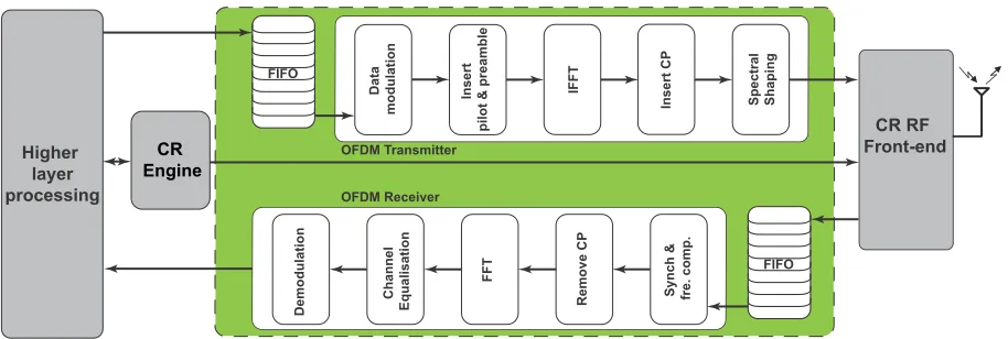
FIGURE 1. Generic structure of multi-standard OFDM cognitive radio system.
years, OFDM has also been adopted as the base modulation scheme for a number of wireless standards in different fre-quency bands, and has been investigated in terms of spectrum sensing and carrier allocation for CR [13], [14]. A radio capable of supporting different OFDM configurations can thus support a wide range of existing and emerging standards.
A. OFDM STANDARDS
[image:4.576.36.275.547.650.2]In this paper, we use three different OFDM standards to demonstrate our prototype multi-standard baseband OFDM transceiver architecture. The system supports not just symbol-by-symbol carrier selection within each standard band, but can switch between standards operating in different fre-quency bands. The system complies with different OFDM symbol lengths and frame formats, according to the three selected standards: IEEE 802.11 [15], IEEE 802.16 [16], and IEEE 802.22 [17]. The relevant specifications for each of these are summarised in Table 1. Further standards with parameters within the bounds of those shown are inherently supported, while other standards can be accommodated with minimal design modification.
TABLE 1. Specifications of three common OFDM-based IEEE standards.
B. SYSTEM REQUIREMENTS
The generic structure of an OFDM transceiver is presented in Figure 1, showing data being modulated, formatted, passed through an inverse fast Fourier transform (FFT), a cyclic
prefix (CP) added, and then being shaped before transmis-sion. The receive chain consists of timing synchronisation and frequency offset compensation, followed by cyclic pre-fix (CP) stripping, FFT, timing correction, and demodula-tion. Such an architecture can be made to support the three OFDM standards in Table 1 by adjusting the baseband oper-ating parameters for each standard (e.g. different sampling frequencies, different sized FFTs, subcarrier modulation, and so on).
Figure 1 also shows the cognitive radio (CR) engine which senses the spectral environment to control the system. This is used to sense unused spectrum and direct the radio to operate in less crowded frequencies. It should determine the best con-figuration, then instruct the baseband to adapt by, for exam-ple, swapping channel frequency, selecting and deselecting different active subcarriers and sampling at a different rate. This can potentially occur on a symbol-by-symbol basis. The architecture we propose is not limited to any particular CR engine, however we demonstrate one hosted on a processor attached to (or embedded within) the FPGA.
III. CHALLENGES IN MULTI-STANDARD RADIO SYSTEMS
In this section we discuss the implementation of an OFDM system for cognitive radio in general, and then consider the particular challenges encountered in supporting multiple standards, for which solutions will be further discussed and evaluated in Section IV.
1) FLEXIBILITY
The chosen OFDM standards span a wide configuration space. For example, referring to Table 1, the FFT/IFFT blocks in each system range in length from 64 to 2048 samples, while the number of carriers ranges from 48 to 1440. Hence, it is necessary to support different FFT window sizes. Traditional static hardware implementation would entail a design con-taining all possible alternatives and the use of multiplexers to switch between them. But since FPGAs are capable of being reconfigured dynamically at runtime, this does not require all circuits to be implemented simultaneously, hence saving area. Furthermore, some processing blocks, like the FFT, can be designed to be intrinsically flexible, offering faster switch-ing at the cost of marginally increased area consumption. Configurability beyond initial expectations is also something to be considered in the real world; a radio built with flexibility in mind should be tolerant to adding new specifications.
2) RECONFIGURATION TIME
The time taken to react to changes in the channel is a critical metric in CR design. While a part of this is composed of the decision making process in the cognitive engine, the configuration latency, once a switching decision has been taken, is also important. In a static multiplexed system, recon-figuration entails selection using multiplexers and so is very fast. However, as discussed previously, this results in a large area overhead since all circuits must be continually present on-chip. Partial reconfiguration allows parts of the FPGA to be replaced at runtime, and can be used to replace the whole baseband chain or individual blocks. Since reconfig-uration time increases as a larger area is reconfigured, careful consideration is required to minimise the size of reconfig-urable blocks. Individual parametrised blocks can change mode quickly, but themselves entail area overhead and design complexity to accommodate the parametrisation.
3) SYNCHRONISATION
There is a key challenge at baseband related to synchronisa-tion. OFDM systems typically tolerate only a small carrier frequency offset (CFO), leading to strict constraints on the design of the RF front-end. In a multi-standard CR, the RF front-end needs to access a wide bandwidth to cover the supported standards, and be able to switch between frequen-cies on a symbol-by-symbol basis. Such a precise and yet wide ranging RF front-end can be very expensive to imple-ment precisely in hardware. This can be overcome through improved synchronisation methods in the baseband hardware, as in [18].
4) SPECTRAL SHAPING
CRs also demand minimised spectral leakage for both in-band and out-of-band transmitted signals. This is man-dated by standards bodies but is also a requirement for the efficient use (or reuse) of nearby unoccupied carriers. OFDM is known to be susceptible to spectral leakage and thus
particular care must be taken to mitigate against this. A fixed spectral mask using RF hardware filtering is not agile in either frequency range or in mask shape, nor is it flexible enough to adapt to changing operating conditions even within a single frequency band, such as selection and deselection of subcarri-ers and adjustments in transmission power. Hence, enhanced techniques for controlling spectral leakage are required [19].
5) DATA INTERFACE
The interface between the baseband and CR engine is another important factor in the implementation of FPGA-based CRs. Many existing hardware radio platforms are extremely diffi-cult to design with, and hence, only hardware experts can use them. While optimisation of low level blocks is necessary, this should be abstracted away from higher layers. A control inter-face to the cognitive engine needs to provide a high level view of the baseband and allow the higher layers to be designed in software with abstracted APIs supporting feedback from and control of the baseband layer.
IV. PROPOSED MULTI-STANDARD OFDM BASEBAND
A. SYSTEM OUTLINE
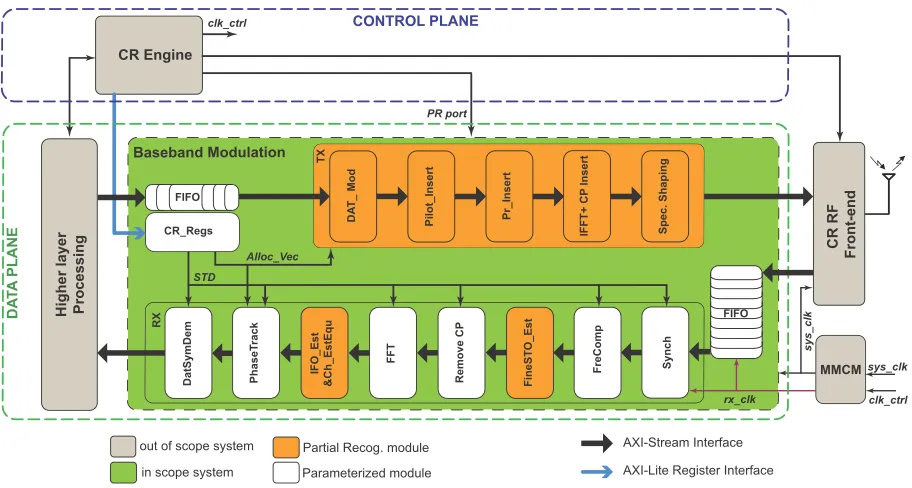
The structure of the proposed OFDM system is illustrated in Figure 2. The baseband modulation implementation must be able to transcieve non-contiguous OFDM (NC-OFDM) signals, as required for a multi-standard radio, supporting different OFDM symbol lengths and frame formats specified according to multiple standards such as IEEE 802.11, 802.16, and 802.22 [15]–[17], as summarised earlier in Table 1.
The CR architecture is divided into a control plane and a data plane. The data plane tranceives data streams to/from the RF front end through two AXI (Advanced eXtensible Interface) stream interfaces. For transmission, data is sent from higher layers and modulated by the data plane. Then modulated sample streams are transferred to the RF front-end to convert to analogue signals and subsequently be up-converted to RF before transmission. For the receiver, the received signal is down-converted to the baseband followed by analogue to digital conversion to form the incoming sam-ple stream. This is then demodulated and processed in the data plane before the data is transferred to the higher layer for processing.
FIGURE 2. Structure of the reconfigurable and parameterised multi-standard CR system.
inter-module communication in the data plane as well as for communication with the higher layers. The AXI-Stream protocol also reduces the requirement for buffering, hence optimising resource usage and total power consumption [20]. Within the processing structure, each module has one slave interface to receive data from the previous module and one master interface to send processed data to the subsequent module.
The baseband data plane is designed to operate in burst mode where it transmits packets as soon as data is available, as well as using flow control to buffer data synchronously. If a data packet is ready to be processed but reconfiguration is in progress, it is stored in a FIFO buffer, then flushed out for processing as soon as reconfiguration is complete. Since the resource requirements for the transmitter are sig-nificantly less than the receiver, reconfiguration time is also much shorter, and there is consequently no loss of trans-mitted packets in the case of PR. Hence, for the transmit-ter, a single monolithic PR region is adopted to support the different standards. The much larger receiver subsys-tem, by contrast, needs to continuously receive and process data packets. The longer reconfiguration time would cause packet loss unless mitigated by buffering. Hence a large FIFO would be needed to store received samples from the RF front end during reconfiguration, but this is problematic since it results in significant additional resource usage. Combining PR and parametrisation, allows us to trade-off buffer require-ments against parametrisation overheads and select a desired balance point.
The control plane contains a cognitive radio (CR) engine that is required to perform adaptation based on the require-ments of the application, ultimately deciding which baseband
standard to use at any point in time, and which sub-carriers to enable for each timeslot. An AXI-Lite register interface between the control and data planes allows status to be inter-preted and parameters to be set using registers in the hardware fabric. The CR engine also includes the PR controller that is responsible for loading bitstreams stored in DRAM into the corresponding PR regions through the ICAP (Internal Configuration Access Port) interface [21] when necessary. Such a control plane can be implemented in a number of ways. It can be standalone software running on a soft pro-cessor core, or implemented in hardware in a separate part of the FPGA. By ensuring that symbol data is processed through a data plane independently of the control plane, we are able to achieve high throughput as well as abstract the data processing away from the control software. Note that the control plane implementation is out of scope for this paper, though the interface defined is generic enough to support different implementations. In the simulation, we have man-ually recreated the control pathways that would be provided by a full control plane, and generated the same control plane messaging to instruct and modify the baseband and module parameters.
In the meantime, the CR engine configures parametrised modules and sets relevant parameters in theCR_Regsregister such as allocation vectors (Alloc_vec), symbol modulation type (MOD), and standard (STD).
The transmission hardware is much simpler than the receiver so will not be detailed here, save to mention incorpo-ration of the advanced spectral shaping approach [19] used to minimize interference around selected subcarriers as needed for a multi-standard CR. We now discuss the receiver base-band modules briefly, indicating how they are designed to be flexible.
B. SYNCHRONISATION
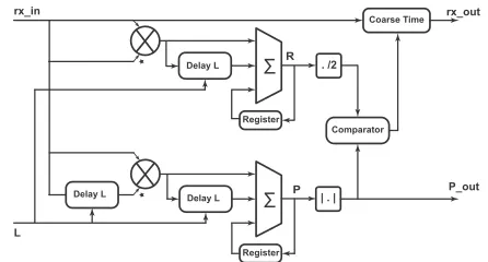
To support burst mode, the CR system must detect the pres-ence of a frame and estimate the frequency offset required based only upon the available burst data, i.e. just using the received frame preamble. The module therefore performs estimation based on the timing parameters, defined in [22],
P(d)= L−1
X
m=0
(rd∗+mrd+m+L)
R(d)= L−1
X
m=0
|rd+m+L|2 (1)
[image:7.576.305.528.63.183.2]whered denotes a time sequential index of received samples r,L is the periodic length of the short preamble, ∗denotes complex conjugation.
TABLE 2. Supported parameter space, with the configurations of the three supported standards shown.
In the proposed approach, lengthLis parametrised so that the module can effectively support the three standards as well as other combinations that might be needed in future standards. This is shown in Table 2, which maps the config-uration space in terms of FFT sizes and lengths and iden-tifies the positions of the three target standards. Figure 3 shows a block diagram of its parametrised implementation. The timing metrics are calculated using auto-correlation on received samples. Coarse Time detects the new frame and roughly estimates the start of a frame using blind estimation that provides generality to support multiple standards.
C. FREQUENCY COMPENSATION
TheFreCompmodule performs fractional carrier frequency offset (CFO) estimation based on the value ofPpassed from
FIGURE 3. Block diagram of Synchronisation module.
theSynchmodule. Fractional CFO estimation and compensa-tion are defined as,
c
1f =
6 P
2πL
d
r(d) =r(d)e−j2π1cf d (2)
where1cf is the estimated fractional CFO,6 Pdenotes the
angle of P, andN is the FFT length. In hardware implemen-tation, a phase rotation sub-module is used to compensate fractional CFO by rotating the received sample phase by the correct angle. This is calculated and accumulated based on estimated fractional CFO.
φ(d)=φ(d−1)+
6 P
L
d
r(d)=r(d)e−jφ(d) (3)
[image:7.576.50.264.442.540.2]According to (3), the computation ofFreCompdepends on the periodic length of the short preamble that is used to calculate P. Assuming that L is normally defined with a power of two value, the division byLcan be computed using a right shift. Figure 4 illustrates the proposed block diagram of parametrised module for frequency compensation. This mod-ule can be effectively implemented to support the required standards by using a shifter that supports these value ofL.
FIGURE 4. Block diagram of frequency compensation module.
D. FINE STO ESTIMATION
[image:7.576.343.493.528.630.2]FIGURE 5. Block diagram of fine STO estimation module.
that is robust to high integer CFO. The metric for fine STO estimation is:
S(d)= L−1
X
m=0
|rd+m+L|2|am|2, (4)
when|am|denotes the normalised amplitude of the preamble at the transmitter. Figure 5 presents the proposed block dia-gram of the fine STO estimation module.Peak Detect finds the maximum value of the correlation that is employed to accurately estimate the STO and Fine Timedetermines the exact first sample of the next OFDM symbol (long preamble symbol). The metric defined in (4) is calculated based on a multiplierless correlation between received samples and the transmitted preamble [23] since cross correlation using full multiplication would be extremely costly in terms of resources. Multiplierless correlation cannot support multi-ple standards in its most efficient form since the hardware implemented depends entirely on the fixed preamble, which is different for each standard. Thus fine STO Estimation is implemented using a PR module. Each supported standard results in a separate partial bitstream that must be reconfig-ured in the PR region at runtime by the CR engine when the underlying standard is switched. Future standards can be supported after deployment by simply generating the required partial bitstream based on the defined preamble.
E. REMOVE CYCLIC PREFIX
RemoveCPremoves the cyclic prefix attached to each OFDM symbol, and this module depends on the length of CPLCPthat is different for each standard.RemoveCPconsists of a counter to count from the beginning of each symbol and remove the CP samples if the counted value is smaller than LCP This module is parametrised by adjustingLCPto support multiple standards.
F. FFT
We use the highly efficient Xilinx FFT/IFFT IP core which supports modification of the FFT length at runtime to cater for different standards. When the length is changed,FFT is modified using the relevant input and the change completes within a few clock cycles. The module always occupies an area sufficient for the largest FFT size required, but its flexi-bility means minimal reconfiguration time.
G. IFO ESTIMATION AND CHANNEL EQUALISATION IFO_Est&Ch_EstEqu corrects IFO and performs channel equalisation. IFO results in a cyclic shift in the frequency domain. The IFO can be determined with robustness to
FIGURE 6.The block diagram of IFO estimation and channel equalisation.
frequency selective channels using correlation on the second (long) preamble [24], [25],
ˆ
=argmax ˜
NFFT−1
X
k=0
Y∗(k−1)Y(k)X∗(k− ˜)X(k−1− ˜)
(5)
where denotes the value of IFO, ˆ, ˜ are esti-mated and trial values of , respectively, Y(k) and X(k) denote the kth frequency symbol index of the received subcarriers and the known transmitted pream-ble, respectively, and the OFDM symbol size NFFT is equal to the FFT size. Figure 6 presents the pro-posed block diagram of the IFO estimation and channel equalisation module.IFO Correctionis performed by cycli-cally shifting OFDM symbols corresponding to the estimated IFO. After compensating for IFO, the effect of the channel can be estimated using information from the second preamble symbol. The estimation and compensation of channel and residual effects can be expressed as:
Y(k)=X(k)∗H(k)+N(k)
ˆ
H(k)= Y(k)
X(k) (6)
ˆ
R(k)= R(k) ˆ
H(k) (7)
H(n) represents the channel effect and N(k) is the AWGN. The equalization taps are estimated in (6), and the compen-sation for received data carriers is given in (7) in which R(k),Rˆ(k) denote received and compensated data carriers, respectively. Since QPSK sub-carrier modulation is used for this proof of concept, amplitude is not a concern. Thus the complex division of channel estimation and compensation can be equivalently performed by multiplying by the conju-gation ofX[k] andHˆ[k], respectively.
This module depends on the second preamble that is specified differently for each standard. Hence, the IFO_Est&Ch_EstEqumodule is implemented as a PR mod-ule to obtain effective standard-specific implementations. Again, this requires that the CR engine load the required partial bitsream at runtime.
H. PHASE TRACKING
[image:8.576.302.530.66.121.2]on received pilots and is computed as
Pk,l =cosθl−α.k.sinθl+j(sinθl−α.k.cosθl), (8)
wherePk,ldenotes the phase of the received pilot which has frequency indexk in thelth OFDM symbol.cosθl +jsinθl is the residual common phase error of the lth OFDM sym-bol, andαis the slope of the phase distortion. The residual common phase error is generally estimated for the supported standards using,
cosθl = 1 NP
X
k∈SP
<{Pk,l}, (9)
sinθl = 1
NP
X
k∈SP
={Pk,l},
[image:9.576.37.278.294.354.2]whereNPdenotes the number of received pilots employed for estimation,SPis the set of used pilot frequency indices.
FIGURE 7. Block diagram of phase tracking module.
According to (9),NPcan be parametrised to support multi-ple standards. Figure 7 presents the proposed block diagram of the parametrised PhaseTrack module.Pilot Extract finds the employed pilots for phase tracking in the OFDM symbol based on the allocation vector (Alloc.Bits).Phase Accumu-lator computes the residual common phase error. The phase error is compensated for by multiplying the data carriers by the complex conjugate of the estimated common phase error.
I. DATA SYMBOL DEMODULATION (DatSymDem)
In the final step, the received bits are extracted from the data symbol by a demodulation block namedDatSymDem. In the present implementation, this only supports QPSK modulation but can be extended to support different data symbol mod-ulations such as 16-QAM or 64-QAM in future, using the same basic interface and parametrisation. All data symbols go through this module, and 2 bits are assigned to the output according to the signed bits of the real and imaginary parts of the data symbol.
J. FIFO BUFFER (FIFO)
FIFOs are needed in the transmitter and in the receiver to buffer data received from the higher layer and the RF front end, respectively. The FIFO buffers are implemented using Xilinx FIFO IP cores that efficiently use BlockRAMs, with 2 port AXI stream interface configuration. During normal operation, one data word is written to the buffer by the higher layer/RF front end, while one is read out from the buffer by the transmitter/receiver in each system clock cycle.
[image:9.576.317.518.309.409.2]Therefore, the FIFO buffers normally operate in an almost empty state. When reconfiguration is required to switch base-band standard, transmit and receive processing are temporar-ily suspended and the FIFOs store incoming data streams. The buffer for the transmitter is less critical than the receiver since transmission operates in burst mode with gaps between frames, however the receiver must process continuously in order to detect incoming frames, perform synchronisation, and correction. This means that there is little spare time to flush data that has been buffered in the receive FIFOs during reconfiguration. Therefore, the receiver FIFO is configured with independent clocks as shown in Figure 8 to allow the clock manager to increase the receive processing rate (rx_clk) to be higher than the sampling rate of the RF front end to help empty the FIFO faster. Once the receiver FIFO is almost empty the processing rate is returned to the sampling rate to reduce power consumption. Since the FIFO IP cores support independent write and read clocks, this functionality is seamless to the stream processing.
FIGURE 8. Receiver FIFO module.
K. MIXED-MODE CLOCK MANAGER (MMCM)
To support this flushing of FIFOs and ‘‘catch up’’ with the delayed received samples, the clock rates need to be adjusted. A Mixed-Mode Clock Manager (MMCM) is used for this purpose, which is able to temporarily increase the processing clock (rec_clk) frequency. The sampling clock rate is also adjusted as required to switch between standards. Increasing operating speed is done by instructing the MMCM module to adjust the frequency of the input clock of the receiving modules,rx_clk. Because these modules, when implemented on FPGA fabric, are able to operate at a frequency higher than 2×the operating clock, no additional resources are consumed in supporting this increased frequency. We benefit from con-tinual improvements in FPGA architecture that mean higher frequencies are achievable than typically required for base-band processing, often even greater than 2×normal rate.
Once the FIFOs are empty, the clock speed is reduced back to the sampling rate (sys_clk) to reduce power consumption. As mentioned, the MMCM module also needs to change the processing rate of the data plane according to the various sam-pling rates specified by different standards, shown in Table 1.
V. PERFORMANCE ANALYSIS
The individual modules and baseband configurations were tested for functional correctness through detailed simulation and comparison with MATLAB prototypes. These served to provide the implementation definition as well as a source for both random and non-random test vectors for each mod-ule. Common input test vectors were used as inputs to OFDM modulation in both implementations and testbench scripts stored resultant output vectors that were compared in MATLAB. The performance of the specific algorithms used for synchronisation was evaluated in MATLAB with both AWGN and frequency selective channels, as discussed in [18], [23], and [25].
The focus of this paper is on the reconfiguration capability, so we will now explore this in detail. We are interested in trade-offs between reconfiguration time and area consump-tion, and how this affects the characteristics of the flexible baseband.
A. ANALYSING LATENCY AND HALTING TIME OF PR MODULES
One crucial challenge when implementing CR systems on reconfigurable hardware is long reconfiguration time when modifying the baseband configurations. PR can take a sig-nificant amount of time, especially for a large monolithic module. In the case of a monolithic CR receiver, the sys-tem would have to stall during reconfiguration, potentially causing the loss of data packets and possibly even loss of synchronisation. A large FIFO would be needed to store the stream of received samples long enough to prevent data loss. A longer reconfiguration time would demand a larger FIFO, resulting in significantly increased hardware resource and power consumption. Another approach often taken is to leave frame losses to be dealt with by higher layers, however this makes sense only in situations where the transmitter and receiver are following compatible protocols.
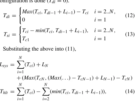
[image:10.576.294.535.63.289.2]We analyse the system to evaluate the latency for a monolithic PR design, as well as for a system employ-ing a finer granularity with multiple PR modules, and a mix of PR and parametrised modules. Figure 9 illustrates the system latency for a system with a monolithic PR module and for one with finer granularity having multi-ple smaller PR modules. We consider a system consisting of N modules. Tc refers to the reconfiguration time. The system or module cannot process data during its recon-figuration time. Li is the computation latency of the nth module. Received data can, of course, be processed during
FIGURE 9. Block diagram illustrating the effect of reconfigurable region size on system latency.
the computation latency. In the case of a large monolithic PR module, the latency, Lsys, and halting time, Thlt that require a FIFO to buffer the received data which would otherwise be lost, is calculated as
Lsys=Tc+ N
X
i=1 (Li)
Thlt =Tc, (10)
Finer granularity is possible by dividing the system into multiple sub-modules, each of which is implemented in a separate PR region. When a module completes configuration, it can process received data while the following module is configured. Note that only one module can be configured at a time due to the presence of only one configuration interface. Therefore, the system reconfiguration latency and halting time for the case of multiple PR modules can be calculated as
Lsys = N
X
i=1
(Tci)+TdN+LN
Thlt = N
X
i=1
(Tsi), (11)
configuration is done (Tdi=0).
Tdi =
(
Max(Tci,Tdi−1+Li−1)−Tci i=2..N,
0 i=1 (12)
Tsi =
(
Tci−min(Tci,Tdi−1+Li−1), i=2..N, Tc1 i=1
(13)
Substituting the above into (11),
Lsys= N
X
i=1
(Tci)+LN
+(Max(TcN,(Max(. . .)−TcN−1)+LN−1)−TcN)
Thlt = N
X
i=1 (Tci)−
N
X
i=2
(min(Tci,Tdi−1+Li−1)), (14)
We can see that system reconfiguration latency and halting time in the case of multiple PR modules is theoretically reduced thanks to being able to overlap the reconfiguration and data processing periods. Practically, the reconfiguration times are usually significantly greater than the processing latencies. This leads toTdi=0 andmin(Tci,Tdi−1+Li−1)= Li−1resulting in an approximated equation for (14):
Lsys = N
X
i=1
(Tci)+LN
Thlt = N
X
i=1 (Tci)−
N−1
X
i=1
(Li), (15)
In addition, because of optimisations in hardware compi-lation, the overhead of partitioning into multiple PR mod-ules leads to the fact that PN
i=1(Tci) is greater than Tc, in (10). Therefore, the system latency,Lsys, and halting time, Thlt in (14) may be greater than that in (10). Generally, the finer granularity approach can only achieve efficiency in terms of the system latency and halting time, if the gain of overlapping the reconfiguration and data processing is greater than the overhead of partitioning into multiple PR modules.
Hence, we propose to mix PR modules and parametrised modules in our flexible baseband to obtain a significant reduction in system reconfiguration latency and halting time. Parametrised modules have the benefit of much faster switch-ing between modes than with PR operation, but if the oper-ating modes are very different, can result in a large area overhead. For each module in the processing chain, com-monalities across different operation modes are analysed and for modules requiring only minor modifications to the data-path, parametrised versions are created. If theithmodule is parametrised, the configuration time of this module can be eliminated because the it can switch operating mode within a few clock periods. This approximately results in the following simplified equations:
Tci ≈0
Tsi≈0
Tdi ≈Tdi−1+Li−1, (16)
The above equations show the increasing efficiency of overlapping reconfiguration and data processing leading to significant reduction in the system latency and halting time.
B. FULL OFDM BASEBAND ANALYSIS
We analyse the results of applying this method to the full receiver baseband of the proposed system, when implemented on a Xilinx Virtex 6 FPGA (XC6VLX240T). We compare a large monolithic PR module, finer granularity PR, and the proposed mixture of PR and parametrisation. Slot based PR is widely used and the only method supported by Xilinx and Altera tools, and hence we employ it. One if its limi-tations is that all resources in the slot are consumed by any module occupying the slot, regardless of whether it actu-ally uses these components or not. The configuration time for a module also depends entirely on the slot size, even if it is using only a fraction of the slot’s resources. There has been some research on alternative methods that reduce resource wastage by allowing more fine-grained reconfigura-tion, hence also reducing reconfiguration time [27]. However, these approaches support a limited number of FPGA devices, require significant engineering effort and expertise to port, and remain unsupported in official tool flows. Furthermore, these improvements may still not benefit overall reconfig-uration latency because this depends on worst case latency (i.e., the reconfiguration time of the largest components).
[image:11.576.41.278.69.249.2]To determine the reconfiguration time of a PR module, we generated bitstreams for all modules required for our baseband design. The area of a PR region must satisfy the needs of the largest mode it will host. For the monolithic PR module, it is required that the PR module be able to contain the full 802.22 OFDM baseband implementation, which is the largest receiver implementation among the three target implementations.
TABLE 3.FPGA resource usage for the 802.22 OFDM baseband.
FIGURE 10. Bitstream sizes for the PR modules.
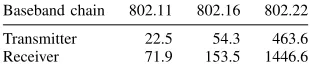
TABLE 4. Baseband chain latencies inµs.
equalisation, phase tracking, data symbol demodulation, respectively.MR,MT are the monolithic receiver and trans-mitter sub-systems, respectively.
We determine the bitstream size for each functional block according to the number of occupied CLB, DSP, BRAM columns that provide sufficient required resources for the block in a rectangular region on the FPGA floorplan. This granularity is necessary to satisfy the requirements of the PR toolflow [28]. Figure 10 illustrates the bitstream sizes of each PR module, which determines reconfiguration time. The bit-stream sizes of the sub-modules are relatively small compared to the monolithic PR module for the receiver sub-system. The M3bitstream is the largest among the sub-modules and the bitstream size of the receiver is almost three times the size of the transmitter.
The overall latency of the transmit and receive chains for the different standards is shown in Table 4 and demonstrates the benefits of an FPGA hardware baseband. Such latencies cannot be achieved using a software baseband running on top of an operating system or even real-time operating system.
Processing latencies for the individual modules are shown for the three standards in Figure 11. We can see that 802.11 has the shortest latency because this standard uses the shortest FFT length, and hence the shortest symbol length for OFDM modulation.
[image:12.576.301.533.282.465.2]It should be noted that during this latency the module still receives input data for processing. The processing chain must be halted when the latency elapses but the reconfiguration of the subsequent module has not yet been completed, as discussed in Section V-A. The configuration time of a PR module is determined based on the size of PR region regard-less operating standard. The PR region must be able to contain the largest module among the three target modules for three
FIGURE 11. Baseband module processing latencies for the three standards.
FIGURE 12. Configuration times and processing latencies for baseband modules for the 802.11 baseband.
standards. Therefore, the worst case halting time occurs for the case of switching baseband to an operating standard with functional modules with the shortest latency.
Partial reconfiguration is performed using a high through-put ICAP controller that supports a data rate of 380 Mbps, close to the theoretical limit of the FPGA [21]. We use a sampling frequency of 10 MHz (i.e. clock period of 0.1µs that is typically defined for the 802.11p standard. Compute latency is calculated for the 802.11 standard, as shown in Fig-ure 12. As can be seen, the module latency is very small in comparison to configuration time in all cases. It is thus clear that overlapping reconfiguration and data processing is not sufficient to overcome reconfiguration delay completely, and so the finer granularity approach may not improve signifi-cantly over a monolithic PR module.
[image:12.576.79.234.288.323.2]FIGURE 13. Transmission scenario requiring reconfiguration.
of the synchronisation module depends on the time when a new frame is detected, the timing offset must be taken into account. Given the transmission scenario shown in Figure 13, when a standard switch is required, both the transmitter and receiver take time to reconfigure the system to the new oper-ating standard. In the proposed receiver, the synchronisation module is a parametrised module, so reconfigures quickly – within a few clock periods – and hence quickly process input samples. However, a new frame cannot be sent quickly because the transmitter is still being reconfigured, resulting in a timing offset in the receiver. It is thus reasonable that the minimum timing offset can be chosen as the configuration time of the transmitter with hardware characteristics reported in Table 3.
C. COMPARISON WITH CONVENTIONAL APPROACHES
[image:13.576.38.276.64.135.2]We have investigated the proposed approach in terms of halt-ing time, FIFO capacity requirements, and reconfiguration latency compared to conventional approaches such as using multiple PR modules and monolithic PR for the whole chain as typically used in FPGA-based dynamic radios [8], [11]. It is worth noting that even these PR approaches remain somewhat specialist due to the design challenge associated with PR design on FPGAs.Mon,Mul,Prodenote the results for the monolithic PR approach, the multiple PR approach, and the proposed approach, respectively.
FIGURE 14. Halting time comparison of the three approaches.
Figure 14 shows the system halting time of the three approaches when the baseband changes operating standard to 802.11, 802.16, and 802.22. The longest halting time of the
FIGURE 15. Halting time breakdown for the three approaches.
three approaches is when the baseband is switched to operate in 802.11 standard. Figure 15 presents the halting time of functional modules in the three approaches for the worse case (i.e. the longest halting time).Tsnis the halting time of the correspondingMnfunctional module.TsRis the halting time of the monolithic receiver sub-system.
We can see from Figure 15 that the halting time of the multiple PR baseband is in fact greater than that of the mono-lithic PR baseband, because the gain achieved by overlapping the reconfiguration and data processing is less than the area overhead of partitioning into multiple PR modules.
This PR area overhead is due to the use of multiple PR regions. Each functional module in the processing chain is assigned to one PR region, even when it is occupies just part of that region. Functional modules can be configured to one of three choices for the three operating standards. The PR region is defined by the largest module among the three. This leads to the sum of multiple PR regions being larger than when using a monolithic PR region. Hence, the halting time of the fine-grain PR approach can actually end up longer than that of the monolithic PR approach. This comparison is mathematically expressed in (10) and (15).
In the proposed approach, some functional modules in the processing chain are implemented by parametrised modules instead of PR modules, leading to elimination of the recon-figuration time for these PR modules. This is mathematically illustrated in (16), and is important in ensuring that the posed approach improves on the alternatives. In fact, the pro-posed approach significantly reduces halting time, to less than a third of that of the monolithic PR module approach. This results in a significant reduction in FIFO buffer requirements to cover the halting time.
[image:13.576.39.277.489.670.2]FIGURE 16. Comparison of three approaches in terms of the longest halting time and FIFO buffer capacity requirements.
TABLE 5. Memory resources for 32 bit AXI4 interface FIFOs.
[image:14.576.39.277.480.679.2]buffer received data in the duration of the longest halting time to avoid losing data. The FIFO capacity requirement is calculated based on multiplying the sampling frequency by the longest halting time, followed by rounding up to the next power of two, as required for the FIFO buffer IP resources on Xilinx FPGAs. Table 5 reports required resources for 32-bit AXI4 interface FIFO implementation with some dif-ferent available size configurations. The FIFO requirement for the proposed approach is only 16 kilo-samples (KS) while the two other approaches require a FIFO which must store up to 64 KS.
FIGURE 17. System reconfiguration latency for the three approaches.
Figure 17 compares the three approaches in term of reconfiguration latency in cases of switching operating stan-dard to 802.11, 802.16, and 802.22. As can be seen, the
requires long processing latencies). However, forMul, the reconfiguration latencies are the same for the three cases because the processing latency of the functional modules is smaller than their reconfiguration time. In particular, the pro-posed approach decreases reconfiguration latencies in com-parison to others approaches. For 802.22, the reconfiguration latency is reduced by 0.63% and 0.45% compared toMon andMul, respectively. In the case of 802.11, reconfiguration latency is significantly reduced by 68% and 71% compared toMonandMul, respectively.
VI. CONCLUSION AND FUTURE WORK
This paper proposed a design for an efficient multi-standard OFDM baseband for FPGA based cognitive radios. Individ-ual blocks in the transmit and receive chains are designed to support different standard requirements, and improved synchronisation and transmission shaping are incorporated. The proposed system combines parametrized modules and partially reconfigured modules to achieve flexibility while minimizing reconfiguration time. We show that this mix-ture results in a significant reduction of 71% compared to conventional approaches in terms of system reconfiguration latency. To avoid data loss, FIFO buffers are used to store data during reconfiguration, and we show that the proposed approach reduces storage requirements to 25% of other PR approaches. The interface to the higher layer processing was also discussed and shown to be compatible with different implementations of cognitive engines. In future work, we aim to incorporate this baseband design into a full CR platform to enable radio designers to take advantage of this flexibility in dynamic radio experiments.
REFERENCES
[1] Y. Liao, L. Song, Z. Han, and Y. Li, ‘‘Full duplex cognitive radio: A new design paradigm for enhancing spectrum usage,’’IEEE Commun. Mag., vol. 53, no. 5, pp. 138–145, May 2015.
[2] S. K. Sharma, T. E. Bogale, S. Chatzinotas, B. Ottersten, L. B. Le, and X. Wang, ‘‘Cognitive radio techniques under practical imperfections: A survey,’’IEEE Commun. Surveys Tuts., vol. 17, no. 4, pp. 1858–1884, 4th Quart., 2015.
[3] (2009). Free Software Foundation, Inc.GNU Radio—The GNU Software Radio. [Online]. Available: http://www.gnu.org/software/gnuradio [4] J. Dowle, S. H. Kuo, K. Mehrotra, and I. V. McLoughlin,
‘‘FPGA-based MIMO and space-time processing platform,’’EURASIP J. Appl. Signal Process. Special Issue MIMO Implement., vol. 2006, Jan. 2006, Art. no. 34653, doi:10.1155/ASP/2006/34653.
[5] G. J. Minden et al., ‘‘KUAR: A flexible software-defined radio development platform,’’ in Proc. Symp. New Frontiers Dyn. Spectrum Access Netw. (DySPAN), Dublin, Ireland, Apr. 2007, pp. 17–22.
[6] K. Amiri, Y. Sun, P. Murphy, C. Hunter, J. R. Cavallaro, and A. Sabharwal, ‘‘WARP, a unified wireless network testbed for education and research,’’ in Proc. IEEE Int. Conf. Microelectron. Syst. Edu., Jun. 2007, pp. 53–54.
[8] J. Delormeet al., ‘‘A FPGA partial reconfiguration design approach for cognitive radio based on NoC architecture,’’ inProc. Joint 6th Int. IEEE Northeast Workshop Circuits Syst. Conf. (TAISA) (NEWCAS-TAISA), Jun. 2008, pp. 355–358.
[9] P. Athanaset al., ‘‘Wires on demand: Run-time communication synthesis for reconfigurable computing,’’ inProc. Int. Conf. Field Programm. Logic Appl., 2007, pp. 1–6.
[10] J. Lotze, S. A. Fahmy, J. Noguera, B. Ozgul, L. Doyle, and R. Esser, ‘‘Development framework for implementing FPGA-based cognitive net-work nodes,’’ inProc. IEEE Global Telecommun. Conf. (GLOBECOM), Dec. 2009, pp. 1–7.
[11] S. Shreejith, B. Banarjee, K. Vipin, and S. A. Fahmy, ‘‘Dynamic cognitive radios on the Xilinx Zynq hybrid FPGA,’’ inProc. Int. Conf. Cognit. Radio Oriented Wireless Netw., 2015, pp. 427–437.
[12] H. A. Mahmoud, T. Yucek, and H. Arslan, ‘‘OFDM for cognitive radio: Merits and challenges,’’IEEE Wireless Commun., vol. 16, no. 2, pp. 6–15, Apr. 2009.
[13] T. Yucek and H. Arslan, ‘‘A survey of spectrum sensing algorithms for cognitive radio applications,’’IEEE Commun. Surveys Tuts., vol. 11, no. 1, pp. 116–130, 1st Quart., 2009.
[14] Y. Zhang and C. Leung, ‘‘Resource allocation in an OFDM-based cognitive radio system,’’IEEE Trans. Commun., vol. 57, no. 7, pp. 1928–1931, Nov. 2009.
[15] Wireless LAN Medium Access Control (MAC) and Physical Layer (PHY) Specifications, IEEE Standard 802.11, 2005.
[16] IEEE Standard for Local and Metropolitan Area Networks Part16: Air Interface for Fixed Broadband Wireless Access Systems, IEEE Standard 802.16, 2009.
[17] IEEE Standard for Wireless Regional Area Networks Part22:Cognitive Wireless RAN Medium Access Control (MAC) and Physical Layer (PHY) Specifications: Policies and Procedures for Operation in the TV Bands, IEEE Standard 802.22, 2011.
[18] T. H. Pham, I. V. McLoughlin, and S. A. Fahmy, ‘‘Robust and efficient OFDM synchronization for FPGA-based radios,’’Circuits, Syst. Signal Process., vol. 33, no. 8, pp. 2475–2493, 2014.
[19] T. H. Pham, S. A. Fahmy, and I. V. McLoughlin, ‘‘Spectrally efficient emis-sion mask shaping for OFDM cognitive radios,’’Digit. Signal Process., vol. 50, pp. 150–161, Mar. 2016.
[20] Q. Liu, G. A. Constantinides, K. Masselos, and P. Cheung, ‘‘Data-reuse exploration under an on-chip memory constraint for low-power FPGA-based systems,’’ IET Comput. Digit. Techn., vol. 3, no. 3, pp. 235–246, 2009.
[21] K. Vipin and S. A. Fahmy, ‘‘A high speed open source controller for FPGA Partial Reconfiguration,’’ inProc. Int. Conf. Field-Programm. Tech-nol. (FPT), Dec. 2012, pp. 61–66.
[22] T. M. Schmidl and D. C. Cox, ‘‘Robust frequency and timing syn-chronization for OFDM,’’ IEEE Trans. Commun., vol. 45, no. 12, pp. 1613–1621, Dec. 1997.
[23] T. H. Pham, S. A. Fahmy, and I. V. McLoughlin, ‘‘Low-power correlation for IEEE 802.16 OFDM synchronisation on FPGA,’’IEEE Trans. Very Large Scale Integr. (VLSI) Syst., vol. 21, no. 8, pp. 1549–1553, Aug. 2013. [24] M. Park, N. Cho, J. Cho, and D. Hong, ‘‘Robust integer frequency offset estimator with ambiguity of symbol timing offset for OFDM systems,’’ in Proc. Veh. Technol. Conf. (VTC), 2002, pp. 2116–2120.
[25] T. H. Pham, S. A. Fahmy, and I. V. McLoughlin, ‘‘Efficient integer fre-quency offset estimation architecture for enhanced OFDM synchroniza-tion,’’IEEE Trans. Very Large Scale Integr. (VLSI) Syst., vol. 24, no. 4, pp. 1412–1420, Apr. 2016.
[26] A. Troya, K. Maharatna, M. Krstic, E. Grass, U. Jagdhold, and R. Kraemer, ‘‘Efficient inner receiver design for OFDM-based WLAN systems: Algorithm and architecture,’’IEEE Trans. Wireless Commun., vol. 6, no. 4, pp. 1374–1385, Apr. 2007.
[27] A. Sohanghpurwala, P. Athanas, T. Frangieh, and A. Wood, ‘‘OpenPR: An open-source partial-reconfiguration toolkit for Xilinx FPGAs,’’ in Proc. IEEE Int. Symp. Parallel Distrib. Process. Workshops Phd Forum (IPDPSW), May 2011, pp. 228–235.
[28] K. Vipin and S. A. Fahmy, ‘‘Architecture-aware reconfiguration-centric floorplanning for partial reconfiguration,’’ in Reconfigurable Computing: Architectures, Tools and Applications: Applied Reconfigurable Computing (ARC). Springer, 2012. [Online]. Available: https://link.springer.com/book/10.1007/978-3-642-28365-9#page=26
THINH HUNG PHAMreceived the B.S. degree in electrical electronic engineering from the Ho Chi Minh City University of Technology, Vietnam, in 2007, and the M.Sc. degree in embedded sys-tems engineering from the University of Leeds, U.K., in 2010, and the Ph.D. degree from the joint Nanyang Technological University, Technis-che Universitat MunTechnis-chen Program, Singapore, in 2015. He was a Research Associate with the TUM CREATE Centre for Electromobility, Singapore. From 2015 to 2016, he was a Lecturer with the Ho Chi Minh City University of Technology. He is currently a Research Fellow with Nanyang Technolog-ical University.
SUHAIB A. FAHMY(M’01–SM’13) received the M.Eng. degree in information systems engineering and the Ph.D. degree in electrical and electronic engineering from the Imperial College London, U.K., in 2003 and 2007, respectively.
From 2007 to 2009, he was a Research Fel-low with Trinity College Dublin, and a Visiting Research Engineer with the Xilinx Research Labs, Dublin. From 2009 to 2015, he was an Assistant Professor with Nanyang Technological University, Singapore. Since 2015, he has been an Associate Professor with the School of Engineering, University of Warwick, U.K., where he currently leads the Con-nected Systems Research Group. He became a Fellow of The Alan Turing Institute in 2017. His research interests include reconfigurable computing and FPGAs, accelerators in a broad range of applications, and networked embedded systems.
Dr. Fahmy is a Chartered Engineer and a member of the IET and a senior member of the ACM. He was a recipient of the Best Paper Award at the IEEE Conference on Field Programmable Technology in 2012, the IBM Faculty Award in 2013, and the Community Award at the International Conference on Field Programmable Logic and Applications in 2016.