Design
Reference
Advanced Analog Products
August 2002
IMPORTANT NOTICE
Texas Instruments Incorporated and its subsidiaries (TI) reserve the right to make corrections, modifications, enhancements, improvements, and other changes to its products and services at any time and to discontinue any product or service without notice. Customers should obtain the latest relevant information before placing orders and should verify that such information is current and complete. All products are sold subject to TI’s terms and conditions of sale supplied at the time of order acknowledgment.
TI warrants performance of its hardware products to the specifications applicable at the time of sale in accordance with TI’s standard warranty. Testing and other quality control techniques are used to the extent TI deems necessary to support this warranty. Except where mandated by government requirements, testing of all parameters of each product is not necessarily performed. TI assumes no liability for applications assistance or customer product design. Customers are responsible for their products and applications using TI components. To minimize the risks associated with customer products and applications, customers should provide adequate design and operating safeguards.
TI does not warrant or represent that any license, either express or implied, is granted under any TI patent right, copyright, mask work right, or other TI intellectual property right relating to any combination, machine, or process in which TI products or services are used. Information published by TI regarding third party products or services does not constitute a license from TI to use such products or services or a warranty or endorsement thereof. Use of such information may require a license from a third party under the patents or other intellectual property of that third party, or a license from TI under the patents or other intellectual property of TI.
Reproduction of information in TI data books or data sheets is permissible only if reproduction is without alteration and is accompanied by all associated warranties, conditions, limitations, and notices. Reproduction of this information with alteration is an unfair and deceptive business practice. TI is not responsible or liable for such altered documentation.
Resale of TI products or services with statements different from or beyond the parameters stated by TI for that product or service voids all express and any implied warranties for the associated TI product or service and is an unfair and deceptive business practice. TI is not responsible or liable for any such statements.
Mailing Address:
Texas Instruments Post Office Box 655303 Dallas, Texas 75265
i
Forward
Everyone interested in analog electronics should find some value in this book, and an ef-fort has been made to make the material understandable to the relative novice while not too boring for the practicing engineer. Special effort has been taken to ensure that each chapter can stand alone for the reader with the proper background. Of course, this causes redundancy that some people might find boring, but it’s worth the price to enable the satis-faction of a diversified audience.
Start at Chapter 1 if you are a novice, and read through until completion of Chapter 9. After Chapter 9 is completed, the reader can jump to any chapter and be confident that they are prepared for the material. More experienced people such as electronic technicians, digital engineers, and non-electronic engineers can start at Chapter 3 and read through Chapter 9. Senior electronic technicians, electronic engineers, and fledgling analog engi-neers can start anywhere they feel comfortable and read through Chapter 9. Experienced analog engineers should jump to the subject that interests them. Analog gurus should send their additions, corrections, and complaints to me, and if they see something that looks familiar, they should feel complimented that others appreciate their contributions. Chapter 1 is a history and story chapter. It is not required reading for anyone, but it defines the op amp’s place in the world of analog electronics. Chapter 2 reviews some basic phys-ics and develops the fundamental circuit equations that are used throughout the book. Similar equations have been developed in other books, but the presentation here empha-sizes material required for speedy op amp design. The ideal op amp equations are devel-oped in Chapter 3, and this chapter enables the reader to rapidly compute op amp transfer equations including ac response. The emphasis on single power supply systems forces the designer to bias circuits when the inputs are referenced to ground, and Chapter 4 gives a detailed procedure that quickly yields a working solution every time.
Op amps can’t exist without feedback, and feedback has inherent stability problems, so feedback and stability are covered in Chapter 5. Chapters 6 and 7 develop the voltage feedback op amp equations, and they teach the concept of relative stability and com-pensation of potentially unstable op amps. Chapter 8 develops the current feedback op amp equations and discusses current feedback stability. Chapter 9 compares current feedback and voltage feedback op amps. The meat of this book is Chapters 12, 13, and 14 where the reader is shown how design the converter to transducer/actuator interface with the aid of op amps.
Thanks to editor James Karki for his contribution. We never gave him enough time to do detailed editing, so if you find errors or typos, direct them to my attention. Thanks to Ted Thomas, a marketing manager with courage enough to support a book, and big thanks for Alun Roberts who paid for this effort. Thomas Kugelstadt, applications manager, thanks for your support and help.
Also many thanks to the contributing authors, James Karki, Richard Palmer, Thomas Ku-gelstadt, Perry Miller, Bruce Carter, and Richard Cesari who gave generously of their time. Regards,
Contents
iii
Contents
1 The Op Amp’s Place In The World . . . 1-1
2 Review of Circuit Theory . . . 2-1
2.1 Introduction . . . 2-1
2.2 Laws of Physics . . . 2-1
2.3 Voltage Divider Rule . . . 2-3
2.4 Current Divider Rule . . . 2-4
2.5 Thevenin’s Theorem . . . 2-5
2.6 Superposition . . . 2-8
2.7 Calculation of a Saturated Transistor Circuit . . . 2-9
2.8 Transistor Amplifier . . . 2-10
3 Development of the Ideal Op Amp Equations . . . 3-1
3.1 Ideal Op Amp Assumptions . . . 3-1
3.2 The Noninverting Op Amp . . . 3-3
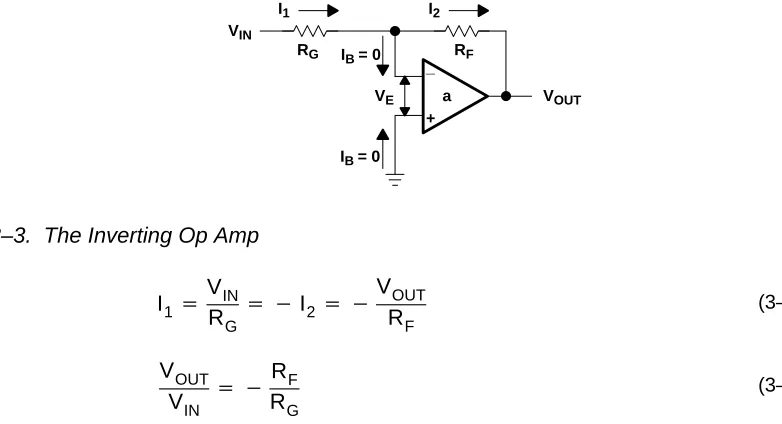
3.3 The Inverting Op Amp . . . 3-4
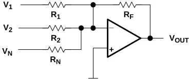
3.4 The Adder . . . 3-5
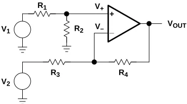
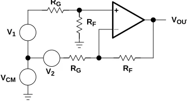
3.5 The Differential Amplifier. . . 3-6
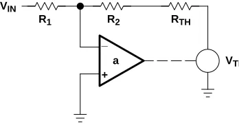
3.6 Complex Feedback Networks . . . 3-7
3.7 Video Amplifiers . . . 3-9
3.8 Capacitors . . . 3-9
3.9 Summary . . . 3-11
4 Single Supply Op Amp Design Techniques . . . 4-1
4.1 Single Supply versus Dual Supply . . . 4-1
4.2 Circuit Analysis . . . 4-3
4.3 Simultaneous Equations . . . 4-8
4.3.1 Case 1: VOUT = +mVIN+b . . . 4-9
4.3.2 Case 2: VOUT = +mVIN – b . . . 4-13
4.3.3 Case 3: VOUT = –mVIN + b . . . 4-16
4.3.4 Case 4: VOUT = –mVIN – b . . . 4-19
4.4 Summary . . . 4-22
5 Feedback and Stability Theory . . . 5-1
5.1 Why Study Feedback Theory? . . . 5-1
5.2 Block Diagram Math and Manipulations. . . 5-1
Contents
5.4 Bode Analysis of Feedback Circuits . . . 5-7
5.5 Loop Gain Plots are the Key to Understanding Stability . . . 5-12
5.6 The Second Order Equation and Ringing/Overshoot Predictions . . . 5-15
5.7 References . . . 5-16
6 Development of the Non Ideal Op Amp Equations. . . 6-1
6.1 Introduction . . . 6-1
6.2 Review of the Canonical Equations . . . 6-2
6.3 Noninverting Op Amps . . . 6-5
6.4 Inverting Op Amps . . . 6-6
6.5 Differential Op Amps . . . 6-8
7 Voltage-Feedback Op Amp Compensation. . . 7-1
7.1 Introduction . . . 7-1
7.2 Internal Compensation . . . 7-2
7.3 External Compensation, Stability, and Performance . . . 7-8
7.4 Dominant-Pole Compensation. . . 7-9
7.5 Gain Compensation . . . 7-12
7.6 Lead Compensation . . . 7-13
7.7 Compensated Attenuator Applied to Op Amp . . . 7-16
7.8 Lead-Lag Compensation . . . 7-18
7.9 Comparison of Compensation Schemes . . . 7-20
7.10 Conclusions. . . 7-21
8 Current-Feedback Op Amp Analysis . . . 8-1
8.1 Introduction . . . 8-1
8.2 CFA Model. . . 8-1
8.3 Development of the Stability Equation . . . 8-2
8.4 The Noninverting CFA . . . 8-3
8.5 The Inverting CFA . . . 8-5
8.6 Stability Analysis . . . 8-7
8.7 Selection of the Feedback Resistor . . . 8-9
8.8 Stability and Input Capacitance. . . 8-11
8.9 Stability and Feedback Capacitance . . . 8-12
8.10 Compensation of CF and CG. . . 8-13
8.11 Summary . . . 8-14
9 Voltage- and Current-Feedback Op Amp Comparison . . . 9-1
9.1 Introduction . . . 9-1
9.2 Precision . . . 9-2
9.3 Bandwidth . . . 9-3
9.4 Stability . . . 9-6
9.5 Impedance . . . 9-7
Contents
v
Contents
10 Op Amp Noise Theory and Applications. . . 10-1
10.1 Introduction . . . 10-1
10.2 Characterization . . . 10-1
10.2.1 rms versus P-P Noise . . . 10-1
10.2.2 Noise Floor . . . 10-3
10.2.3 Signal-to-Noise Ratio . . . 10-3
10.2.4 Multiple Noise Sources . . . 10-3
10.2.5 Noise Units . . . 10-4
10.3 Types of Noise . . . 10-4
10.3.1 Shot Noise . . . 10-5
10.3.2 Thermal Noise . . . 10-7
10.3.3 Flicker Noise . . . 10-8
10.3.4 Burst Noise . . . 10-9
10.3.5 Avalanche Noise . . . 10-9
10.4 Noise Colors . . . 10-10
10.4.1 White Noise . . . 10-11
10.4.2 Pink Noise . . . 10-11
10.4.3 Red/Brown Noise . . . 10-12
10.5 Op Amp Noise . . . 10-12
10.5.1 The Noise Corner Frequency and Total Noise . . . 10-12
10.5.2 The Corner Frequency . . . 10-13
10.5.3 Op Amp Circuit Noise Model . . . 10-14
10.5.4 Inverting Op Amp Circuit Noise . . . 10-16
10.5.5 Noninverting Op Amp Circuit Noise . . . 10-17
10.5.6 Differential Op Amp Circuit Noise . . . 10-18
10.5.7 Summary. . . 10-18
10.6 Putting It All Together . . . 10-19
10.7 References . . . 10-23
11 Understanding Op Amp Parameters . . . 11-1
11.1 Introduction . . . 11-1
11.2 Operational Amplifier Parameter Glossary . . . 11-2
11.3 Additional Parameter Information . . . 11-8
11.3.1 Input Offset Voltage . . . 11-8
11.3.2 Input Current. . . 11-10
11.3.3 Input Common Mode Voltage Range . . . 11-11
11.3.4 Differential Input Voltage Range . . . 11-11
11.3.5 Maximum Output Voltage Swing . . . 11-12
11.3.6 Large Signal Differential Voltage Amplification . . . 11-13
11.3.7 Input Parasitic Elements. . . 11-13
11.3.8 Output Impedance . . . 11-14
11.3.9 Common-Mode Rejection Ratio . . . 11-15
11.3.10 Supply Voltage Rejection Ratio . . . 11-15
Contents
11.3.12 Slew Rate at Unity Gain . . . 11-16
11.3.13 Equivalent Input Noise . . . 11-17
11.3.14 Total Harmonic Distortion Plus Noise. . . 11-18
11.3.15 Unity Gain Bandwidth and Phase Margin . . . 11-19
11.3.16 Settling Time. . . 11-22
12 Instrumentation: Sensors to A/D Converters. . . 12-1
12.1 Introduction . . . 12-1
12.2 Transducer Types . . . 12-6
12.3 Design Procedure . . . 12-11
12.4 Review of the System Specifications . . . 12-12
12.5 Reference Voltage Characterization. . . 12-12
12.6 Transducer Characterization . . . 12-13
12.7 ADC Characterization . . . 12-15
12.8 Op Amp Selection . . . 12-15
12.9 Amplifier Circuit Design. . . 12-16
12.10 Test . . . 12-23
12.11 Summary . . . 12-23
12.12 References . . . 12-23
13 Wireless Communication: Signal Conditioning for IF Sampling . . . 13-1
13.1 Introduction . . . 13-1
13.2 Wireless Systems. . . 13-1
13.3 Selection of ADCs/DACs . . . 13-6
13.4 Factors Influencing the Choice of Op Amps . . . 13-10
13.5 Anti-Aliasing Filters . . . 13-11
13.6 Communication D/A Converter Reconstruction Filter . . . 13-13
13.7 External Vref Circuits for ADCs/DACs . . . 13-15
13.8 High-Speed Analog Input Drive Circuits. . . 13-18
13.9 References . . . 13-22
14 Interfacing D/A Converters to Loads . . . 14-1
14.1 Introduction . . . 14-1
14.2 Load Characteristics . . . 14-1
14.2.1 DC Loads . . . 14-1
14.2.2 AC Loads . . . 14-2
14.3 Understanding the D/A Converter and its Specifications . . . 14-2
14.3.1 Types of D/A Converters — Understanding the Tradeoffs . . . 14-2
14.3.2 The Resistor Ladder D/A Converter . . . 14-2
14.3.3 The Weighted Resistor D/A Converter. . . 14-3
14.3.4 The R/2R D/A Converter . . . 14-4
14.3.5 The Sigma Delta D/A Converter . . . 14-5
14.4 D/A Converter Error Budget . . . 14-6
14.4.1 Accuracy versus Resolution. . . 14-7
Contents
vii
Contents
14.4.3 AC Application Error Budget . . . 14-8
14.4.4 RF Application Error Budget . . . 14-10
14.5 D/A Converter Errors and Parameters . . . 14-10
14.5.1 DC Errors and Parameters. . . 14-10
14.5.2 AC Application Errors and Parameters . . . 14-14
14.6 Compensating For DAC Capacitance . . . 14-18
14.7 Increasing Op Amp Buffer Amplifier Current and Voltage . . . 14-19
14.7.1 Current Boosters . . . 14-20
14.7.2 Voltage Boosters . . . 14-20
14.7.3 Power Boosters . . . 14-22
14.7.4 Single-Supply Operation and DC Offsets . . . 14-22
15 Sine Wave Oscillators. . . 15-1
15.1 What is a Sine Wave Oscillator? . . . 15-1
15.2 Requirements for Oscillation . . . 15-1
15.3 Phase Shift in the Oscillator . . . 15-3
15.4 Gain in the Oscillator . . . 15-4
15.5 Active Element (Op Amp) Impact on the Oscillator . . . 15-5
15.6 Analysis of the Oscillator Operation (Circuit). . . 15-7
15.7 Sine Wave Oscillator Circuits . . . 15-9
15.7.1 Wien Bridge Oscillator . . . 15-9
15.7.2 Phase Shift Oscillator, Single Amplifier . . . 15-14
15.7.3 Phase Shift Oscillator, Buffered. . . 15-15
15.7.4 Bubba Oscillator. . . 15-17
15.7.5 Quadrature Oscillator . . . 15-18
15.7.6 Conclusion . . . 15-20
15.8 References . . . 15-21
16 Active Filter Design Techniques . . . 16-1
16.1 Introduction . . . 16-1
16.2 Fundamentals of Low-Pass Filters . . . 16-2
16.2.1 Butterworth Low-Pass FIlters. . . 16-6
16.2.2 Tschebyscheff Low-Pass Filters . . . 16-7
16.2.3 Bessel Low-Pass Filters . . . 16-7
16.2.4 Quality Factor Q. . . 16-9
16.2.5 Summary. . . 16-10
16.3 Low-Pass Filter Design . . . 16-11
16.3.1 First-Order Low-Pass Filter . . . 16-12
16.3.2 Second-Order Low-Pass Filter . . . 16-14
16.3.3 Higher-Order Low-Pass Filters . . . 16-19
16.4 High-Pass Filter Design . . . 16-21
16.4.1 First-Order High-Pass Filter . . . 16-23
16.4.2 Second-Order High-Pass Filter . . . 16-24
Contents
16.5 Band-Pass Filter Design . . . 16-27
16.5.1 Second-Order Band-Pass Filter . . . 16-29
16.5.2 Fourth-Order Band-Pass Filter (Staggered Tuning). . . 16-32
16.6 Band-Rejection Filter Design . . . 16-36
16.6.1 Active Twin-T Filter . . . 16-37
16.6.2 Active Wien-Robinson Filter. . . 16-39
16.7 All-Pass Filter Design . . . 16-41
16.7.1 First-Order All-Pass Filter. . . 16-44
16.7.2 Second-Order All-Pass Filter. . . 16-44
16.7.3 Higher-Order All-Pass Filter. . . 16-45
16.8 Practical Design Hints . . . 16-47
16.8.1 Filter Circuit Biasing . . . 16-47
16.8.2 Capacitor Selection . . . 16-50
16.8.3 Component Values . . . 16-52
16.8.4 Op Amp Selection . . . 16-53
16.9 Filter Coefficient Tables. . . 16-55
16.10 References . . . 16-63
17 Circuit Board Layout Techniques . . . 17-1
17.1 General Considerations . . . 17-1
17.1.1 The PCB is a Component of the Op Amp Design . . . 17-1
17.1.2 Prototype, Prototype, PROTOTYPE! . . . 17-1
17.1.3 Noise Sources . . . 17-2
17.2 PCB Mechanical Construction . . . 17-3
17.2.1 Materials — Choosing the Right One for the Application . . . 17-3
17.2.2 How Many Layers are Best? . . . 17-4
17.2.3 Board Stack-Up — The Order of Layers . . . 17-6
17.3 Grounding . . . 17-7
17.3.1 The Most Important Rule: Keep Grounds Separate . . . 17-7
17.3.2 Other Ground Rules . . . 17-7
17.3.3 A Good Example . . . 17-9
17.3.4 A Notable Exception . . . 17-10
17.4 The Frequency Characteristics of Passive Components . . . 17-11
17.4.1 Resistors . . . 17-11
17.4.2 Capacitors. . . 17-12
17.4.3 Inductors . . . 17-13
17.4.4 Unexpected PCB Passive Components . . . 17-14
17.5 Decoupling . . . 17-20
17.5.1 Digital Circuitry — A Major Problem for Analog Circuitry . . . 17-20
17.5.2 Choosing the Right Capacitor . . . 17-21
17.5.3 Decoupling at the IC Level. . . 17-22
17.5.4 Decoupling at the Board Level . . . 17-23
17.6 Input and Output Isolation . . . 17-23
Contents
ix
Contents
17.7.1 Through-Hole Considerations . . . 17-26
17.7.2 Surface Mount . . . 17-27
17.7.3 Unused Sections . . . 17-27
17.8 Summary . . . 17-28
17.8.1 General . . . 17-28
17.8.2 Board Structure . . . 17-28
17.8.3 Components . . . 17-28
17.8.4 Routing . . . 17-29
17.8.5 Bypass. . . 17-29
17.9 References . . . 17-29
18 Designing Low-Voltage Op Amp Circuits . . . 18-1
18.1 Introduction . . . 18-1
18.2 Dynamic Range . . . 18-3
18.3 Signal-to-Noise Ratio . . . 18-5
18.4 Input Common-Mode Range . . . 18-6
18.5 Output Voltage Swing . . . 18-11
18.6 Shutdown and Low Current Drain . . . 18-12
18.7 Single-Supply Circuit Design . . . 18-13
18.8 Transducer to ADC Analog Interface . . . 18-13
18.9 DAC to Actuator Analog Interface . . . 18-16
18.10 Comparison of Op Amps . . . 18-20
18.11 Summary . . . 18-22
A Single-Supply Circuit Collection . . . A-1
A.1 Introduction . . . A-1
A.2 Boundary Conditions . . . A-4
A.3 Amplifiers. . . A-5
A.3.1 Inverting Op Amp with Noninverting Positive Reference . . . A-5
A.3.2 Inverting Op Amp with Inverting Negative Reference . . . A-6
A.3.3 Inverting Op Amp with Noninverting Negative Reference . . . A-7
A.3.4 Inverting Op Amp with Inverting Positive Reference . . . A-8
A.3.5 Noninverting Op Amp with Inverting Positive Reference . . . A-9
A.3.6 Noninverting Op Amp with Noninverting Negative Reference . . . A-10
A.3.7 Noninverting Op Amp with Inverting Negative Reference . . . A-11
A.3.8 Noninverting Op Amp with Noninverting Positive Reference . . . A-12
A.3.9 Differential Amplifier . . . A-13
A.3.10 Differential Amplifier With Bias Correction. . . A-14
A.3.11 High Input Impedance Differential Amplifier . . . A-15
A.3.12 High Common-Mode Range Differential Amplifier . . . A-16
A.3.13 High-Precision Differential Amplifier . . . A-17
A.3.14 Simplified High-Precision Differential Amplifier. . . A-18
A.3.15 Variable Gain Differential Amplifier . . . A-19
Contents
A.3.17 Buffer . . . A-21
A.3.18 Inverting AC Amplifier . . . A-22
A.3.19 Noninverting AC Amplifier . . . A-23
A.4 Computing Circuits . . . A-24
A.4.1 Inverting Summer . . . A-24
A.4.2 Noninverting Summer . . . A-25
A.4.3 Noninverting Summer with Buffers . . . A-26
A.4.4 Inverting Integrator . . . A-27
A.4.5 Inverting Integrator with Input Current Compensation. . . A-28
A.4.6 Inverting Integrator with Drift Compensation. . . A-29
A.4.7 Inverting Integrator with Mechanical Reset . . . A-30
A.4.8 Inverting Integrator with Electronic Reset . . . A-31
A.4.9 Inverting Integrator with Resistive Reset . . . A-32
A.4.10 Noninverting Integrator with Inverting Buffer. . . A-33
A.4.11 Noninverting Integrator Approximation . . . A-34
A.4.12 Inverting Differentiator. . . A-35
A.4.13 Inverting Differentiator with Noise Filter. . . A-36
A.5 Oscillators . . . A-37
A.5.1 Basic Wien Bridge Oscillator . . . A-37
A.5.2 Wien Bridge Oscillator with Nonlinear Feedback . . . A-38
A.5.3 Wien Bridge Oscillator with AGC . . . A-39
A.5.4 Quadrature Oscillator . . . A-40
A.5.5 Classical Phase Shift Oscillator. . . A-41
A.5.6 Buffered Phase Shift Oscillator . . . A-42
A.5.7 Bubba Oscillator. . . A-43
A.5.8 Triangle Oscillator . . . A-44
Figures
xi
Contents
Figures
2–1 Ohm’s Law Applied to the Total Circuit . . . 2-2
2–2 Ohm’s Law Applied to a Component . . . 2-2
2–3 Kirchoff’s Voltage Law . . . 2-2
2–4 Kirchoff’s Current Law . . . 2-3
2–5 Voltage Divider Rule. . . 2-3
2–6 Current Divider Rule. . . 2-4
2–7 Original Circuit . . . 2-5
2–8 Thevenin’s Equivalent Circuit for Figure 2–7 . . . 2-5
2–9 Example of Thevenin’s Equivalent Circuit . . . 2-6
2–10 Analysis Done the Hard Way . . . 2-7
2–11 Superposition Example . . . 2-8
2–12 When V1 is Grounded . . . 2-8
2–13 When V2 is Grounded . . . 2-8
2–14 Saturated Transistor Circuit. . . 2-9
2–15 Transistor Amplifier. . . 2-10
2–16 Thevenin Equivalent of the Base Circuit . . . 2-11
3–1 The Ideal Op Amp. . . 3-2
3–2 The Noninverting Op Amp . . . 3-3
3–3 The Inverting Op Amp . . . 3-4
3–4 The Adder Circuit . . . 3-5
3–5 The Differential Amplifier . . . 3-6
3–6 Differential Amplifier With Common-Mode Input Signal . . . 3-7
3–7 T Network in Feedback Loop . . . 3-7
3–8 Thevenin’s Theorem Applied to T Network . . . 3-8
3–9 Video Amplifier . . . 3-9
3–10 Low-Pass Filter . . . 3-10
3–11 High-Pass Filter. . . 3-10
4–1 Split-Supply Op Amp Circuit . . . 4-1
4–2 Split-Supply Op Amp Circuit With Reference Voltage Input . . . 4-2
4–3 Split-Supply Op Amp Circuit With Common-Mode Voltage . . . 4-2
4–4 Single-Supply Op Amp Circuit . . . 4-3
4–5 Inverting Op Amp . . . 4-4
4–6 Inverting Op Amp With VCC Bias . . . 4-5
4–7 Transfer Curve for Inverting Op Amp With VCC Bias . . . 4-5
Figures
4–9 Transfer Curve for Noninverting Op Amp . . . 4-7
4–10 Schematic for Case1: VOUT = +mVIN + b. . . 4-9
4–11 Case 1 Example Circuit . . . 4-12
4–12 Case 1 Example Circuit Measured Transfer Curve. . . 4-12
4–13 Schematic for Case 2: VOUT = +mVIN – b . . . 4-13
4–14 Case 2 Example Circuit . . . 4-15
4–15 Case 2 Example Circuit Measured Transfer Curve. . . 4-15
4–16 Schematic for Case 3: VOUT = –mVIN + b . . . 4-16
4–17 Case 3 Example Circuit . . . 4-17
4–18 Case 3 Example Circuit Measured Transfer Curve. . . 4-18
4–19 Schematic for Case 4: VOUT = –mVIN – b . . . 4-19
4–20 Case 4 Example Circuit . . . 4-20
4–21 Case 4 Example Circuit Measured Transfer Curve. . . 4-21
5–1 Definition of Blocks . . . 5-2
5–2 Summary Points . . . 5-3
5–3 Definition of Control System Terms . . . 5-3
5–4 Definition of an Electronic Feedback Circuit. . . 5-3
5–5 Multiloop Feedback System . . . 5-4
5–6 Block Diagram Transforms . . . 5-5
5–7 Comparison of Control and Electronic Canonical Feedback Systems . . . 5-6
5–8 Low-Pass Filter . . . 5-8
5–9 Bode Plot of Low-Pass Filter Transfer Function . . . 5-9
5–10 Band Reject Filter . . . 5-9
5–11 Individual Pole Zero Plot of Band Reject Filter . . . 5-10
5–12 Combined Pole Zero Plot of Band Reject Filter . . . 5-10
5–13 When No Pole Exists in Equation (5–12) . . . 5-11
5–14 When Equation 5–12 has a Single Pole . . . 5-11
5–15 Magnitude and Phase Plot of Equation 5–14. . . 5-13
5–16 Magnitude and Phase Plot of the Loop Gain Increased to (K+C). . . 5-14
5–17 Magnitude and Phase Plot of the Loop Gain With Pole Spacing Reduced . . . 5-14
5–18 Phase Margin and Overshoot vs Damping Ratio . . . 5-16
6–1 Feedback System Block Diagram . . . 6-2
6–2 Feedback Loop Broken to Calculate Loop Gain . . . 6-4
6–3 Noninverting Op Amp. . . 6-5
6–4 Open Loop Noninverting Op Amp . . . 6-6
6–5 Inverting Op Amp . . . 6-6
6–6 Inverting Op Amp: Feedback Loop Broken for Loop Gain Calculation . . . 6-7
6–7 Differential Amplifier Circuit . . . 6-8
7–1 Miller Effect Compensation . . . 7-2
7–2 TL03X Frequency and Time Response Plots . . . 7-3
7–3 Phase Margin and Percent Overshoot Versus Damping Ratio . . . 7-4
Figures
xiii
Contents
7–5 TL08X Frequency and Time Response Plots . . . 7-6
7–6 TLV277X Frequency Response Plots . . . 7-7
7–7 TLV227X Time Response Plots . . . 7-7
7–8 Capacitively-Loaded Op Amp . . . 7-9
7–9 Capacitively-Loaded Op Amp With Loop Broken for Loop Gain (Aβ) Calculation . . . 7-9
7–10 Possible Bode Plot of the Op Amp Described in Equation 7–7. . . 7-11
7–11 Dominant-Pole Compensation Plot . . . 7-11
7–12 Gain Compensation . . . 7-12
7–13 Lead-Compensation Circuit. . . 7-13
7–14 Lead-Compensation Bode Plot. . . 7-14
7–15 Inverting Op Amp With Lead Compensation . . . 7-15
7–16 Noninverting Op Amp With Lead Compensation. . . 7-16
7–17 Op Amp With Stray Capacitance on the Inverting Input. . . 7-16
7–18 Compensated Attenuator Circuit . . . 7-17
7–19 Compensated Attenuator Bode Plot . . . 7-18
7–20 Lead-Lag Compensated Op Amp . . . 7-19
7–21 Bode Plot of Lead-Lag Compensated Op Amp . . . 7-19
7–22 Closed-Loop Plot of Lead-Lag Compensated Op Amp . . . 7-20
8–1 Current-Feedback Amplifier Model . . . 8-2
8–2 Stability Analysis Circuit. . . 8-2
8–3 Stability Analysis Circuit. . . 8-3
8–4 Noninverting CFA . . . 8-4
8–5 Inverting CFA. . . 8-5
8–6 Bode Plot of Stability Equation . . . 8-7
8–7 Plot of CFA RF, G, and BW . . . 8-10
8–8 Effects of Stray Capacitance on CFAs . . . 8-12
8–9 Bode Plot with CF . . . 8-13
9–1 Long-Tailed Pair . . . 9-2
9–2 Ideal CFA . . . 9-3
9–3 VFA Gain versus Frequency . . . 9-4
9–4 CFA Gain vs Frequency. . . 9-5
10–1 Gaussian Distribution of Noise Energy . . . 10-2
10–2 Shot Noise Generation. . . 10-5
10–3 Thermal Noise . . . 10-7
10–4 Avalanche Noise . . . 10-10
10–5 Noise Colors . . . 10-11
10–6 TLV2772 Op Amp Noise Characteristics . . . 10-13
10–7 Op Amp Circuit Noise Model. . . 10-15
10–8 Equivalent Op Amp Circuit Noise Model. . . 10-15
10–9 Inverting Op Amp Circuit Noise Model . . . 10-16
10–10 Inverting Equivalent Op Amp Circuit Noise Model . . . 10-16
Figures
10–12 Differential Equivalent Op Amp Circuit Noise Model. . . 10-18
10–13 Split Supply Op Amp Circuit . . . 10-19
10–14 TLC2201 Op Amp Noise Performance . . . 10-20
10–15 TLC2201 Op Amp Circuit . . . 10-21
10–16 Improved TLC2201 Op Amp Circuit. . . 10-23
11–1 Test Circuits for Input Offset Voltage . . . 11-9
11–2 Offset Voltage Adjust . . . 11-9
11–3 Test Circuit – IIB . . . 11-10
11–4 VOM± . . . 11-12
11–5 Input Parasitic Elements . . . 11-13
11–6 Effect of Output Impedance . . . 11-14
11–7 Figure 6. Slew Rate . . . 11-16
11–8 Figure 7. Simplified Op Amp Schematic . . . 11-17
11–9 Typical Op amp Input Noise Spectrum . . . 11-18
11–10 Output Spectrum with THD + N = 1% . . . 11-19
11–11 Voltage Amplification and Phase Shift vs. Frequency . . . 11-21
11–12 Settling Time . . . 11-22
12–1 Block Diagram of a Transducer Measurement System . . . 12-1
12–2 Significant Bits versus Binary Bits . . . 12-2
12–3 Example of Spans That Require Correction. . . 12-4
12–4 Voltage Divider Circuit for a Resistive Transducer . . . 12-6
12–5 Current Source Excitation for a Resistive Transducer . . . 12-7
12–6 Precision Current Source . . . 12-7
12–7 Wheatstone Bridge Circuit. . . 12-8
12–8 Photodiode Amplifier . . . 12-8
12–9 Phototransistor Amplifier . . . 12-9
12–10 Photovoltaic Cell Amplifier. . . 12-9
12–11 Active Full-Wave Rectifier and Filter . . . 12-10
12–12 Reference and Transducer Bias Circuit . . . 12-13
12–13 AIA Circuit . . . 12-17
12–14 Final Analog Interface Circuit . . . 12-21
13–1 A Typical GSM Cellular Base Station Receiver Block Diagram . . . 13-2
13–2 An Implementation of a Software-Configurable Dual-IF Receiver . . . 13-4
13–3 Basic W-CDMA Cellular Base Station Transmitter Block. . . 13-5
13–4 Communication DAC with Interpolation and Reconstruction Filters. . . 13-5
13–5 QPSK Power Spectral Density Without Raised Cosine Filter — W-CDMA . . . 13-14
13–6 Reconstruction Filter Characteristics. . . 13-14
13–7 A Single-Pole Reconstruction Filter . . . 13-15
13–8 Voltage Reference Filter Circuit . . . 13-16
13–9 Voltage Follower Frequency Response Plot . . . 13-17
13–10 External Voltage Reference Circuit for ADC/DAC. . . 13-17
Figures
xv
Contents
13–12 Differential Amplifier Closed-Loop Response . . . 13-19
13–13 ADC Single-Ended Input Drive Circuit. . . 13-20
13–14 Gain vs Frequency Plot for THS3201 . . . 13-21
13–15 Phase vs Frequency for THS3201. . . 13-21
14–1 Resistor Ladder D/A Converter . . . 14-2
14–2 Binary Weighted D/A Converter . . . 14-3
14–3 R/2R Resistor Array . . . 14-4
14–4 R/2R D/A Converter . . . 14-5
14–5 Sigma Delta D/A Converter. . . 14-6
14–6 Total Harmonic Distortion . . . 14-9
14–7 D/A Offset Error. . . 14-11
14–8 D/A Gain Error . . . 14-12
14–9 Differential Nonlinearity Error . . . 14-13
14–10 Integral Nonlinearity Error . . . 14-13
14–11 Spurious Free Dynamic Range . . . 14-15
14–12 Intermodulation Distortion . . . 14-16
14–13 D/A Settling Time . . . 14-17
14–14 D/A Deglitch Circuit . . . 14-17
14–15 Compensating for CMOS DAC Output Capacitance . . . 14-18
14–16 D/A Output Current Booster . . . 14-20
14–17 Incorrect Method of Increasing Voltage Swing of D/A Converters . . . 14-21
14–18 Correct Method of Increasing Voltage Range . . . 14-22
14–19 Single-Supply DAC Operation . . . 14-23
15–1 Canonical Form of a Feedback System with Positive or Negative Feedback . . . 15-2
15–2 Phase Plot of RC Sections . . . 15-3
15–3 Op Amp Frequency Response . . . 15-6
15–4 Op Amp Bandwidth and Oscillator Output . . . 15-7
15–5 Block Diagram of an Oscillator with Positive Feedback . . . 15-8
15–6 Amplifier with Positive and Negative Feedback. . . 15-8
15–7 Wien Bridge Circuit Schematic . . . 15-9
15–8 Final Wien Bridge Oscillator Circuit . . . 15-11
15–9 Wien Bridge Output Waveforms . . . 15-11
15–10 Wien Bridge Oscillator with Nonlinear Feedback . . . 15-12
15–11 Output of the Circuit in Figure 15–10. . . 15-12
15–12 Wien Bridge Oscillator with AGC . . . 15-13
15–13 Output of the Circuit in Figure 15–12. . . 15-14
15–14 Phase Shift Oscillator (Single Op Amp) . . . 15-14
15–15 Output of the Circuit in Figure 15–14. . . 15-15
15–16 Phase Shift Oscillator, Buffered . . . 15-16
15–17 Output of the Circuit Figure 15–16. . . 15-16
15–18 Bubba Oscillator . . . 15-17
Figures
15–20 Quadrature Oscillator . . . 15-19
15–21 Output of the Circuit in Figure 15–20. . . 15-20
16–1 Second-Order Passive Low-Pass and Second-Order Active Low-Pass . . . 16-1
16–2 First-Order Passive RC Low-Pass. . . 16-2
16–3 Fourth-Order Passive RC Low-Pass with Decoupling Amplifiers . . . 16-3
16–4 Frequency and Phase Responses of a Fourth-Order Passive RC Low-Pass Filter . . . . 16-4
16–5 Amplitude Responses of Butterworth Low-Pass Filters . . . 16-6
16–6 Gain Responses of Tschebyscheff Low-Pass Filters . . . 16-7
16–7 Comparison of Phase Responses of Fourth-Order Low-Pass Filters . . . 16-8
16–8 Comparison of Normalized Group Delay (Tgr) of Fourth-Order Low-Pass Filters. . . 16-8
16–9 Comparison of Gain Responses of Fourth-Order Low-Pass Filters. . . 16-9
16–10 Graphical Presentation of Quality Factor Q on a Tenth-Order
Tschebyscheff Low-Pass Filter with 3-dB Passband Ripple . . . 16-10
16–11 Cascading Filter Stages for Higher-Order Filters . . . 16-12
16–12 First-Order Noninverting Low-Pass Filter . . . 16-12
16–13 First-Order Inverting Low-Pass Filter. . . 16-13
16–14 First-Order Noninverting Low-Pass Filter with Unity Gain . . . 16-14
16–15 General Sallen-Key Low-Pass Filter . . . 16-15
16–16 Unity-Gain Sallen-Key Low-Pass Filter. . . 16-15
16–17 Second-Order Unity-Gain Tschebyscheff Low-Pass with 3-dB Ripple. . . 16-16
16–18 Adjustable Second-Order Low-Pass Filter . . . 16-17
16–19 Second-Order MFB Low-Pass Filter . . . 16-18
16–20 First-Order Unity-Gain Low-Pass . . . 16-19
16–21 Second-Order Unity-Gain Sallen-Key Low-Pass Filter. . . 16-20
16–22 Fifth-Order Unity-Gain Butterworth Low-Pass Filter . . . 16-21
16–23 Low-Pass to High-Pass Transition Through Components Exchange . . . 16-21
16–24 Developing The Gain Response of a High-Pass Filter . . . 16-22
16–25 First-Order Noninverting High-Pass Filter. . . 16-23
16–26 First-Order Inverting High-Pass Filter . . . 16-23
16–27 General Sallen-Key High-Pass Filter. . . 16-24
16–28 Unity-Gain Sallen-Key High-Pass Filter . . . 16-24
16–29 Second-Order MFB High-Pass Filter. . . 16-25
16–30 Third-Order Unity-Gain Bessel High-Pass . . . 16-27
16–31 Low-Pass to Band-Pass Transition . . . 16-28
16–32 Gain Response of a Second-Order Band-Pass Filter. . . 16-29
16–33 Sallen-Key Band-Pass . . . 16-30
16–34 MFB Band-Pass . . . 16-31
16–35 Gain Responses of a Fourth-Order Butterworth Band-Pass and its Partial Filters . . . . 16-36
16–36 Low-Pass to Band-Rejection Transition . . . 16-37
16–37 Passive Twin-T Filter . . . 16-37
16–38 Active Twin-T Filter . . . 16-38
16–39 Passive Wien-Robinson Bridge . . . 16-39
Figures
xvii
Contents
16–41 Comparison of Q Between Passive and Active Band-Rejection Filters. . . 16-41
16–42 Frequency Response of the Group Delay for the First 10 Filter Orders . . . 16-43
16–43 First-Order All-Pass . . . 16-44
16–44 Second-Order All-Pass Filter . . . 16-44
16–45 Seventh-Order All-Pass Filter. . . 16-46
16–46 Dual-Supply Filter Circuit. . . 16-47
16–47 Single-Supply Filter Circuit . . . 16-47
16–48 Biasing a Sallen-Key Low-Pass . . . 16-48
16–49 Biasing a Second-Order MFB Low-Pass Filter . . . 16-49
16–50 Biasing a Sallen-Key and an MFB High-Pass Filter . . . 16-50
16–51 Differences in Q and fC in the Partial Filters of an Eighth-Order Butterworth
Low-Pass Filter . . . 16-51
16–52 Modification of the Intended Butterworth Response to aTschebyscheff-Type
Characteristic. . . 16-51
16–53 Open-Loop Gain (AOL) and Filter Response (A) . . . 16-53
17–1 Op Amp Terminal Model . . . 17-5
17–2 Digital and Analog Plane Placement . . . 17-8
17–3 Separate Grounds . . . 17-8
17–4 Broadcasting From PCB Traces. . . 17-9
17–5 A Careful Board Layout . . . 17-10
17–6 Resistor High-Frequency Performance. . . 17-11
17–7 Capacitor High-Frequency Performance . . . 17-12
17–8 Inductor High-Frequency Performance . . . 17-13
17–9 Loop and Slot Antenna Board Trace Layouts . . . 17-15
17–10 PCB Trace Corners . . . 17-16
17–11 PCB Trace-to-Plane Capacitance Formula . . . 17-17
17–12 Effect of 1-pF Capacitance on Op Amp Inverting Input . . . 17-18
17–13 Coupling Between Parallel Signal Traces. . . 17-19
17–14 Via Inductance Measurements . . . 17-19
17–15 Logic Gate Output Structure . . . 17-21
17–16 Capacitor Self Resonance. . . 17-22
17–17 Common Op Amp Pinouts. . . 17-24
17–18 Trace Length for an Inverting Op Amp Stage . . . 17-25
17–19 Mirror-Image Layout for Quad Op Amp Package . . . 17-25
17–20 Quad Op Amp Package Layout with Half-Supply Generator . . . 17-26
17–21 Proper Termination of Unused Op Amp Sections . . . 17-28
18–1 Op Amp Error Sources. . . 18-4
18–2 Noninverting Op Amp . . . 18-7
18–3 Input Circuit of a NonRRI Op Amp. . . 18-8
18–4 Input Circuit of an RRI Op Amp . . . 18-8
18–5 Input Bias Current Changes with Input Common-Mode Voltage . . . 18-9
Figures
18–7 RRO Output Stage . . . 18-11
18–8 Data Acquisition System . . . 18-14
18–9 Schematic for the Transducer to ADC Interface Circuit . . . 18-15
18–10 Final Schematic for the Transducer to ADC Interface Circuit . . . 18-16
18–11 Digital Control System . . . 18-16
18–12 DAC Current Source to Actuator Interface Circuit. . . 18-17
18–13 DAC Current Sink to Actuator Interface Circuit . . . 18-19
A–1 Split-Supply Op Amp Circuit . . . A-1
A–2 Split-Supply Op Amp Circuit With Reference Voltage Input . . . A-2
A–3 Split-Supply Op Amp Circuit With Common-Mode Voltage . . . A-3
A–4 Single-Supply Op Amp Circuit . . . A-3
A–5 Inverting Op Amp with Noninverting Positive Reference . . . A-5
A–6 Inverting Op Amp with Inverting Negative Reference. . . A-6
A–7 Inverting Op Amp with Noninverting Negative Reference . . . A-7
A–8 Inverting Op Amp with Inverting Positive Reference. . . A-8
A–9 Noninverting Op Amp with Inverting Positive Reference . . . A-9
A–10 Noninverting Op Amp with Noninverting Negative Reference . . . A-10
A–11 Noninverting Op Amp with Inverting Positive Reference . . . A-11
A–12 Noninverting Op Amp with Noninverting Positive Reference . . . A-12
A–13 Differential Amplifier . . . A-13
A–14 Differential Amplifier with Bias Correction. . . A-14
A–15 High Input Impedance Differential Amplifier. . . A-15
A–16 High Common-Mode Range Differential Amplifier . . . A-16
A–17 High-Precision Differential Amplifier . . . A-17
A–18 Simplified High-Precision Differential Amplifier . . . A-18
A–19 Variable Gain Differential Amplifier . . . A-19
A–20 T Network in the Feedback Loop . . . A-20
A–21 Buffer. . . A-21
A–22 Inverting AC Amplifier . . . A-22
A–23 Noninverting AC Amplifier . . . A-23
A–24 Inverting Summer . . . A-24
A–25 Noninverting Summer . . . A-25
A–26 Noninverting Summer with Buffers . . . A-26
A–27 Inverting Integrator . . . A-27
A–28 Inverting Integrator with Input Current Compensation . . . A-28
A–29 Inverting Integrator with Drift Compensation . . . A-29
A–30 Inverting Integrator with Mechanical Reset . . . A-30
A–31 Inverting Integrator with Electronic Reset. . . A-31
A–32 Inverting Integrator with Resistive Reset . . . A-32
A–33 Noninverting Integrator with Inverting Buffer . . . A-33
A–34 Noninverting Integrator Approximation . . . A-34
A–35 Inverting Differentiator . . . A-35
Figures
xix
Contents
A–37 Basic Wien Bridge Oscillator. . . A-37
A–38 Wien Bridge Oscillator with Nonlinear Feedback . . . A-38
A–39 Wien Bridge Oscillator with AGC . . . A-39
A–40 Quadrature Oscillator . . . A-40
A–41 Classical Phase Shift Oscillator . . . A-41
A–42 Buffered Phase Shift Oscillator. . . A-42
A–43 Bubba Oscillator . . . A-43
Tables
Tables
3–1 Basic Ideal Op Amp Assumptions . . . 3-2
8–1 Data Set for Curves in Figure 8–7 . . . 8-11
9–1 Tabulation of Pertinent VFA and CFA Equations. . . 9-9
10–1 Noise Colors . . . 10-10
11–1 Op Amp Parameter GLossary . . . 11-2
11–2 Cross-Reference of Op Amp Parameters. . . 11-6
12–1 Transducer Output Voltage . . . 12-14
12–2 ADC Input Voltage . . . 12-15
12–3 Op Amp Selection. . . 12-16
12–4 AIA Input and Output Voltages . . . 12-16
12–5 Offset and Gain Error Budget . . . 12-19
13–1 GSM Receiver Block System Budget . . . 13-3
13–2 High-Speed Op Amp Requirements . . . 13-11
14–1 DC Step Size for D/A converters . . . 14-7
14–2 Converter Bits, THD, and Dynamic Range. . . 14-10
16–1 Second-Order FIlter Coefficients . . . 16-17
16–2 Values of α For Different Filter Types and Different Qs . . . 16-33
16–3 Single-Supply Op Amp Selection Guide (TA = 25°C, VCC = 5 V) . . . 16-54
16–4 Bessel Coefficients . . . 16-56
16–5 Butterworth Coefficients. . . 16-57
16–6 Tschebyscheff Coefficients for 0.5-dB Passband Ripple . . . 16-58
16–7 Tschebyscheff Coefficients for 1-dB Passband Ripple . . . 16-59
16–8 Tschebyscheff Coefficients for 2-dB Passband Ripple . . . 16-60
16–9 Tschebyscheff Coefficients for 3-dB Passband Ripple . . . 16-61
16–10 All-Pass Coefficients. . . 16-62
17–1 PCB Materials . . . 17-3
17–2 Recommended Maximum Frequencies for Capacitors . . . 17-21
18–1 Comparison of Op Amp Error Terms . . . 18-5
18–2 Op Amp Parameters. . . 18-21
Examples
xxi
Contents
Examples
16–1 First-Order Unity-Gain Low-Pass Filter . . . 16-14
16–2 Second-Order Unity-Gain Tschebyscheff Low-Pass Filter . . . 16-16
16–3 Fifth-Order Filter . . . 16-19
16–4 Third-Order High-Pass Filter with fC = 1 kHz . . . 16-26
16–5 Second-Order MFB Band-Pass Filter with fm = 1 kHz . . . 16-32
16–6 Fourth-Order Butterworth Band-Pass Filter . . . 16-34
1-1
The Op Amp’s Place In The World
Ron Mancini
In 1934 Harry Black[1] commuted from his home in New York City to work at Bell Labs in New Jersey by way of a railroad/ferry. The ferry ride relaxed Harry enabling him to do some conceptual thinking. Harry had a tough problem to solve; when phone lines were extended long distances, they needed amplifiers, and undependable amplifiers limited phone service. First, initial tolerances on the gain were poor, but that problem was quickly solved with an adjustment. Second, even when an amplifier was adjusted correctly at the factory, the gain drifted so much during field operation that the volume was too low or the incoming speech was distorted.
Many attempts had been made to make a stable amplifier, but temperature changes and power supply voltage extremes experienced on phone lines caused uncontrollable gain drift. Passive components had much better drift characteristics than active components had, thus if an amplifier’s gain could be made dependent on passive components, the problem would be solved. During one of his ferry trips, Harry’s fertile brain conceived a novel solution for the amplifier problem, and he documented the solution while riding on the ferry.
The solution was to first build an amplifier that had more gain than the application re-quired. Then some of the amplifier output signal was fed back to the input in a manner that makes the circuit gain (circuit is the amplifier and feedback components) dependent on the feedback circuit rather than the amplifier gain. Now the circuit gain is dependent on the passive feedback components rather than the active amplifier. This is called negative feedback, and it is the underlying operating principle for all modern day op amps. Harry had documented the first intentional feedback circuit during a ferry ride. I am sure unintentional feedback circuits had been built prior to that time, but the design-ers ignored the effect!
I can hear the squeals of anguish coming from the managers and amplifier designers. I imagine that they said something like this, “it is hard enough to achieve 30-kHz gain– bandwidth (GBW), and now this fool wants me to design an amplifier with 3-MHz GBW. But, he is still going to get a circuit gain GBW of 30 kHz”. Well, time has proven Harry right, but there is a minor problem that Harry didn’t discuss in detail, and that is the oscillation
problem. It seems that circuits designed with large open loop gains sometimes oscillate when the loop is closed. A lot of people investigated the instability effect, and it was pretty well understood in the 1940s, but solving stability problems involved long, tedious, and intricate calculations. Years passed without anybody making the problem solution simpler or more understandable.
In 1945 H. W. Bode presented a system for analyzing the stability of feedback systems by using graphical methods. Until this time, feedback analysis was done by multiplication and division, so calculation of transfer functions was a time consuming and laborious task. Remember, engineers did not have calculators or computers until the ’70s. Bode present-ed a log technique that transformpresent-ed the intensely mathematical process of calculating a feedback system’s stability into graphical analysis that was simple and perceptive. Feed-back system design was still complicated, but it no longer was an art dominated by a few electrical engineers kept in a small dark room. Any electrical engineer could use Bode’s methods to find the stability of a feedback circuit, so the application of feedback to ma-chines began to grow. There really wasn’t much call for electronic feedback design until computers and transducers become of age.
The first real-time computer was the analog computer! This computer used prepro-grammed equations and input data to calculate control actions. The programming was hard wired with a series of circuits that performed math operations on the data, and the hard wiring limitation eventually caused the declining popularity of the analog computer. The heart of the analog computer was a device called an operational amplifier because it could be configured to perform many mathematical operations such as multiplication, addition, subtraction, division, integration, and differentiation on the input signals. The name was shortened to the familiar op amp, as we have come to know and love them. The op amp used an amplifier with a large open loop gain, and when the loop was closed, the amplifier performed the mathematical operations dictated by the external passive components. This amplifier was very large because it was built with vacuum tubes and it required a high-voltage power supply, but it was the heart of the analog computer, thus its large size and huge power requirements were accepted as the price of doing business. Many early op amps were designed for analog computers, and it was soon found out that op amps had other uses and were very handy to have around the physics lab.
1-3
The first signal conditioning op amps were constructed with vacuum tubes prior to the introduction of transistors, so they were large and bulky. During the ’50s, miniature vacu-um tubes that worked from lower voltage power supplies enabled the manufacture of op amps that shrunk to the size of a brick used in house construction, so the op amp modules were nicknamed bricks. Vacuum tube size and component size decreased until an op amp was shrunk to the size of a single octal vacuum tube. Transistors were commercially developed in the ’60s, and they further reduced op amp size to several cubic inches, but the nickname brick still held on. Now the nickname brick is attached to any electronic mod-ule that uses potting compound or non-integrated circuit (IC) packaging methods. Most of these early op amps were made for specific applications, so they were not necessarily general purpose. The early op amps served a specific purpose, but each manufacturer had different specifications and packages; hence, there was little second sourcing among the early op amps.
ICs were developed during the late 1950s and early 1960s, but it wasn’t till the middle
1960s that Fairchild released the µA709. This was the first commercially successful IC
op amp, and Robert J. Widler designed it. The µA709 had its share of problems, but any
competent analog engineer could use it, and it served in many different analog
applica-tions. The major drawback of the µA709 was stability; it required external compensation
and a competent analog engineer to apply it. Also, the µA709 was quite sensitive because
it had a habit of self destructing under any adverse condition. The self-destruction habit was so prevalent that one major military equipment manufacturer published a paper titled
something like, The 12 Pearl Harbor Conditions of the µA709. The µA741 followed the
µA709, and it is an internally compensated op amp that does not require external
com-pensation if operated under data sheet conditions. Also, it is much more forgiving than
the µA709. There has been a never-ending series of new op amps released each year
since then, and their performance and reliability has improved to the point where present day op amps can be used for analog applications by anybody.
The IC op amp is here to stay; the latest generation op amps cover the frequency spec-trum from 5-kHz GBW to beyond 1-GHz GBW. The supply voltage ranges from guaran-teed operation at 0.9 V to absolute maximum voltage ratings of 1000 V. The input current and input offset voltage has fallen so low that customers have problems verifying the specifications during incoming inspection. The op amp has truly become the universal analog IC because it performs all analog tasks. It can function as a line driver, comparator (one bit A/D), amplifier, level shifter, oscillator, filter, signal conditioner, actuator driver, cur-rent source, voltage source, and many other applications. The designer’s problem is how to rapidly select the correct circuit/op amp combination and then, how to calculate the pas-sive component values that yield the desired transfer function in the circuit.
you are looking in the wrong place. The op amp is treated as a completed component in this book.
The op amp will continue to be a vital component of analog design because it is such a fundamental component. Each generation of electronics equipment integrates more functions on silicon and takes more of the analog circuitry inside the IC. Don’t fear, as digi-tal applications increase, analog applications also increase because the predominant supply of data and interface applications are in the real world, and the real world is an ana-log world. Thus, each new generation of electronics equipment creates requirements for new analog circuits; hence, new generations of op amps are required to fulfill these re-quirements. Analog design, and op amp design, is a fundamental skill that will be required far into the future.
References
2-1
Review of Circuit Theory
Ron Mancini
2.1
Introduction
Although this book minimizes math, some algebra is germane to the understanding of analog electronics. Math and physics are presented here in the manner in which they are used later, so no practice exercises are given. For example, after the voltage divider rule is explained, it is used several times in the development of other concepts, and this usage constitutes practice.
Circuits are a mix of passive and active components. The components are arranged in a manner that enables them to perform some desired function. The resulting arrangement of components is called a circuit or sometimes a circuit configuration. The art portion of analog design is developing the circuit configuration. There are many published circuit configurations for almost any circuit task, thus all circuit designers need not be artists. When the design has progressed to the point that a circuit exists, equations must be writ-ten to predict and analyze circuit performance. Textbooks are filled with rigorous methods for equation writing, and this review of circuit theory does not supplant those textbooks. But, a few equations are used so often that they should be memorized, and these equa-tions are considered here.
There are almost as many ways to analyze a circuit as there are electronic engineers, and if the equations are written correctly, all methods yield the same answer. There are some simple ways to analyze the circuit without completing unnecessary calculations, and these methods are illustrated here.
2.2
Laws of Physics
Ohm’s law is stated as V=IR, and it is fundamental to all electronics. Ohm’s law can be applied to a single component, to any group of components, or to a complete circuit. When the current flowing through any portion of a circuit is known, the voltage dropped across that portion of the circuit is obtained by multiplying the current times the resistance (Equa-tion 2–1).
Laws of Physics
(2–1)
V+IR
In Figure 2–1, Ohm’s law is applied to the total circuit. The current, (I) flows through the total resistance (R), and the voltage (V) is dropped across R.
V R
I
Figure 2–1. Ohm’s Law Applied to the Total Circuit
In Figure 2–2, Ohm’s law is applied to a single component. The current (IR) flows through
the resistor (R) and the voltage (VR) is dropped across R. Notice, the same formula is used
to calculate the voltage drop across R even though it is only a part of the circuit.
V R
IR
VR
Figure 2–2. Ohm’s Law Applied to a Component
Kirchoff’s voltage law states that the sum of the voltage drops in a series circuit equals the sum of the voltage sources. Otherwise, the source (or sources) voltage must be dropped across the passive components. When taking sums keep in mind that the sum is an algebraic quantity. Kirchoff’s voltage law is illustrated in Figure 2–3 and Equations 2–2 and 2–3.
V R2
R1
VR1
VR2
Figure 2–3. Kirchoff’s Voltage Law
(2–2)
ȍ
VSOURCES+ȍ
VDROPS(2–3)
V+VR1)VR2
Voltage Divider Rule
2-3
Review of Circuit Theory
source, through a component, or through a wire, because all currents are treated identi-cally. Kirchoff’s current law is illustrated in Figure 2–4 and Equations 2–4 and 2–5.
I4 I3
I1 I2
Figure 2–4. Kirchoff’s Current Law
(2–4)
ȍ
IIN+ȍ
IOUT(2–5)
I1)I2+I3)I4
2.3
Voltage Divider Rule
When the output of a circuit is not loaded, the voltage divider rule can be used to calculate the circuit’s output voltage. Assume that the same current flows through all circuit
ele-ments (Figure 2–5). Equation 2–6 is written using Ohm’s law as V = I (R1 + R2). Equation
2–7 is written as Ohm’s law across the output resistor.
V R2
I
VO
R1
I
Figure 2–5. Voltage Divider Rule
(2–6)
I+ V
R1)R2
(2–7)
VOUT+IR2
Substituting Equation 2–6 into Equation 2–7, and using algebraic manipulation yields Equation 2–8.
(2–8)
VOUT+V R2 R1)R2
out-Current Divider Rule
put voltage. Remember that the voltage divider rule always assumes that the output resis-tor is not loaded; the equation is not valid when the output resisresis-tor is loaded by a parallel component. Fortunately, most circuits following a voltage divider are input circuits, and input circuits are usually high resistance circuits. When a fixed load is in parallel with the output resistor, the equivalent parallel value comprised of the output resistor and loading resistor can be used in the voltage divider calculations with no error. Many people ignore the load resistor if it is ten times greater than the output resistor value, but this calculation can lead to a 10% error.
2.4
Current Divider Rule
When the output of a circuit is not loaded, the current divider rule can be used to calculate
the current flow in the output branch circuit (R2). The currents I1 and I2 in Figure 2–6 are
assumed to be flowing in the branch circuits. Equation 2–9 is written with the aid of Kirch-off’s current law. The circuit voltage is written in Equation 2–10 with the aid of Ohm’s law. Combining Equations 2–9 and 2–10 yields Equation 2–11.
I R2 V
I2
I1
R1
Figure 2–6. Current Divider Rule
(2–9)
I+I1)I2
(2–10)
V+I1R1+I2R2
(2–11)
I+I1)I2+I2R2
R1)I2+I2
ǒ
R1)R2 R1
Ǔ
Rearranging the terms in Equation 2–11 yields Equation 2–12.
(2–12)
I2+I
ǒ
R1 R1)R2Ǔ
The total circuit current divides into two parts, and the resistance (R1) divided by the total
resistance determines how much current flows through R2. An easy method of
Thevenin’s Theorem
2-5
Review of Circuit Theory
2.5
Thevenin’s Theorem
There are times when it is advantageous to isolate a part of the circuit to simplify the analy-sis of the isolated part of the circuit. Rather than write loop or node equations for the com-plete circuit, and solving them simultaneously, Thevenin’s theorem enables us to isolate the part of the circuit we are interested in. We then replace the remaining circuit with a simple series equivalent circuit, thus Thevenin’s theorem simplifies the analysis. There are two theorems that do similar functions. The Thevenin theorem just described is the first, and the second is called Norton’s theorem. Thevenin’s theorem is used when the input source is a voltage source, and Norton’s theorem is used when the input source is a current source. Norton’s theorem is rarely used, so its explanation is left for the reader to dig out of a textbook if it is ever required.
The rules for Thevenin’s theorem start with the component or part of the circuit being
re-placed. Referring to Figure 2–7, look back into the terminals (left from C and R3 toward
point XX in the figure) of the circuit being replaced. Calculate the no load voltage (VTH)
as seen from these terminals (use the voltage divider rule).
V
R3 C R1
R2
X
[image:33.612.256.397.526.612.2]X
Figure 2–7. Original Circuit
Look into the terminals of the circuit being replaced, short independent voltage sources, and calculate the impedance between these terminals. The final step is to substitute the Thevenin equivalent circuit for the part you wanted to replace as shown in Figure 2–8.
VTH
R3
C RTH
X
X
Figure 2–8. Thevenin’s Equivalent Circuit for Figure 2–7
Thevenin’s Theorem
theorem because it eliminates the need for solving several simultaneous equations. The detailed information about what happens in the circuit that was replaced is not available when using Thevenin’s theorem, but that is no consequence because you had no interest in it.
As an example of Thevenin’s theorem, let’s calculate the output voltage (VOUT) shown in
Figure 2–9A. The first step is to stand on the terminals X–Y with your back to the output
circuit, and calculate the open circuit voltage seen (VTH). This is a perfect opportunity to
use the voltage divider rule to obtain Equation 2–13.
V R2 VOUT
R1 R3
X Y
(a) The Original Circuit
VTH VOUT
RTH R3
X Y
(b) The Thevenin Equivalent Circuit
R4 R4
Figure 2–9. Example of Thevenin’s Equivalent Circuit
(2–13)
VTH+V R2 R1)R2
Still standing on the terminals X-Y, step two is to calculate the impedance seen looking into these terminals (short the voltage sources). The Thevenin impedance is the parallel
impedance of R1 and R2 as calculated in Equation 2–14. Now get off the terminals X-Y
before you damage them with your big feet. Step three replaces the circuit to the left of
X-Y with the Thevenin equivalent circuit VTH and RTH.
(2–14)
RTH+ R1R2
R1)R2+R1
Ŧ
R2 Note:Two parallel vertical bars ( || ) are used to indicate parallel components as shown in Equation 2–14.
Thevenin’s Theorem
2-7
Review of Circuit Theory
(2–15)
VOUT+VTH R4
RTH)R3)R4+V
ǒ
R2 R1)R2Ǔ
R4 R1R2
R1)R2
)R3)R4
The circuit analysis is done the hard way in Figure 2–10, so you can see the advantage
of using Thevenin’s Theorem. Two loop currents, I1 and I2, are assigned to the circuit.
Then the loop Equations 2–16 and 2–17 are written.
V
R3
VOUT
I1
R1
I2
R4
R2
Figure 2–10. Analysis Done the Hard Way
(2–16)
V+I1
ǒ
R1)R2Ǔ
*I2R2(2–17)
I2
ǒ
R2)R3)R4Ǔ
+I1R2Equation 2–17 is rewritten as Equation 2–18 and substituted into Equation 2–16 to obtain Equation 2–19.
(2–18)
I1+I2 R2)R3)R4 R2
(2–19)
V+I2
ǒ
R2)R3)R4R2
Ǔ
ǒ
R1)R2Ǔ
*I2R2The terms are rearranged in Equation 2–20. Ohm’s law is used to write Equation 2–21, and the final substitutions are made in Equation 2–22.
(2–20)
I2 + V
R2)R3)R4
R2
ǒ
R1)R2Ǔ
*R2(2–21)
VOUT+I2R4
(2–22)
VOUT+V R4
ǒR
2)R3)R4Ǔ ǒR
1)R2Ǔ
R2
*R2
Superposition
2.6
Superposition
Superposition is a theorem that can be applied to any linear circuit. Essentially, when there are independent sources, the voltages and currents resulting from each source can be calculated separately, and the results are added algebraically. This simplifies the cal-culations because it eliminates the need to write a series of loop or node equations. An example is shown in Figure 2–11.
V1 VOUT
R1
R2
R3
V2
Figure 2–11.Superposition Example
When V1 is grounded, V2 forms a voltage divider with R3 and the parallel combination of
R2 and R1. The output voltage for this circuit (VOUT2) is calculated with the aid of the
volt-age divider equation (2–23). The circuit is shown in Figure 2–12. The voltvolt-age divider rule yields the answer quickly.
V2 V
OUT2
R3
R2
R1
Figure 2–12. When V1 is Grounded
(2–23)
VOUT2+V2 R1øR2 R3)R1øR2
Likewise, when V2 is grounded (Figure 2–13), V1 forms a voltage divider with R1 and the
parallel combination of R3 and R2, and the voltage divider theorem is applied again to
cal-culate VOUT (Equation 2–24).
V1 V
OUT1
R1
R2
R3
Calculation of a Saturated Transistor Circuit
2-9
Review of Circuit Theory
(2–24)
VOUT1+V1 R2ø R3 R1)R2øR3
After the calculations for each source are made the components are added to obtain the final solution (Equation 2–25).
(2–25)
VOUT+V1 R2øR3
R1)R2øR3)V2
R1øR2 R3)R1øR2
The reader should analyze this circuit with loop or node equations to gain an appreciation for superposition. Again, the superposition results come out as a simple arrangement that is easy to understand. One looks at the final equation and it is obvious that if the sources
are equal and opposite polarity, and when R1 = R3, then the output voltage is zero.
Conclu-sions such as this are hard to make after the results of a loop or node analysis unless con-siderable effort is made to manipulate the final equation into symmetrical form.
2.7
Calculation of a Saturated Transistor Circuit
The circuit specifications are: when VIN = 12 V, VOUT <0.4 V at ISINK <10 mA, and VIN <0.05
V, VOUT >10 V at IOUT = 1 mA. The circuit diagram is shown in Figure 2–14.
IC 12 V
VOUT
IB
RB
VIN
RC
Figure 2–14. Saturated Transistor Circuit
The collector resistor must be sized (Equation 2–26) when the transistor is off, because it has to be small enough to allow the output current to flow through it without dropping more than two volts to meet the specification for a 10-V output.
(2–26)
RCvV)12*VOUT
IOUT +
12*10
1 + 2 k
Transistor Amplifier
(2–27)
IC+bIB+V)12*VCE
RC )IL[
V)12 RC )IL
(2–28)
RBvVIN*VBE IB
Substituting Equation 2–27 into Equation 2–28 yields Equation 2–29.
(2–29)
RBv
ǒ
VIN*VBEǓ
bIC +
(12*0.6)50 V
ƪ
122 )(10)
ƫ
mA+35.6 k
When the transistor goes on it sinks the load current, and it still goes into saturation. These calculations neglect some minor details, but they are in the 98% accuracy range.
2.8
Transistor Amplifier
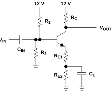
The amplifier is an analog circuit (Figure 2–15), and the calculations, plus the points that must be considered during the design, are more complicated than for a saturated circuit. This extra complication leads people to say that analog design is harder than digital de-sign (the saturated transistor is digital i.e.; on or off). Analog dede-sign is harder than digital design because the designer must account for all states in analog, whereas in digital only two states must be accounted for. The specifications for the amplifier are an ac voltage gain of four and a peak-to-peak signal swing of 4 volts.
12 V
VOUT
VIN
RC
CE RE2
RE1 R1
R2 12 V
[image:38.612.230.411.465.616.2]CIN
Figure 2–15. Transistor Amplifier
IC is selected as 10 mA because the transistor has a current gain (β) of 100 at that point.
Transistor Amplifier
2-11
Review of Circuit Theory
2 V (from 8 V to 10 V) there is still enough voltage dropped across RC to keep the transistor
on. Set the collector-emitter voltage at 4 V; when the collector voltage swings negative 2 V (from 8 V to 6 V) the transistor still has 2 V across it, so it stays linear. This sets the
emitter voltage (VE) at 4 V.
(2–30)
RCvV)12*VC
IC +
12 V*8 V
10 mA + 400W
(2–31)
RE+RE1)RE2+VE IE +
VE IB)IC^
VE IC +
4 V
10 mA+ 400W
Use Thevenin’s equivalent circuit to calculate R1 and R2 as shown in Figure 2–16.
IB R1 || R2
VB = 4.6 V
R2
R1 + R2
[image:39.612.158.539.176.481.2]12
Figure 2–16. Thevenin Equivalent of the Base Circuit
(2–32)
IB+IC
b +10 mA100 +0.1 mA
(2–33)
VTH+ 12R2 R1)R2
(2–34)
RTH+ R1R2 R1)R2
We want the base voltage to be 4.6 V because the emitter voltage is then 4 V. Assume
a voltage drop of 0.4 V across RTH, so Equation 2–35 can be written. The drop across RTH
may not be exactly 0.4 V because of beta variations, but a few hundred mV does not
mat-ter is this design. Now, calculate the ratio of R1 and R2 using the voltage divider rule (the
load current has been accounted for).
(2–35)
RTH+0.4
0.1k+4 k
(2–36)
VTH+IBRTh)VB+0.4)4.6+5+12 R2 R1)R2
(2–37)
R2+7 5 R1
R1 is almost equal to R2, thus selecting R1 as twice the Thevenin resistance yields
Transistor Amplifier
approximately RC/RE1 because CE shorts out RE2 at high frequencies, so we can write
Equation 2–38.
(2–38)
RE1+RC
G +
400
4 + 100W
(2–39)
RE2+RE*RE1+ 400*100+300W
The capacitor selection depends on the frequency response required for the amplifier, but
3-1
Development of the Ideal Op Amp Equations
Ron Mancini
3.1
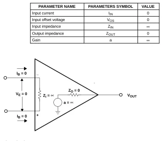
Ideal Op Amp Assumptions
The name Ideal Op Amp is applied to this and similar analysis because the salient param-eters of the op amp are assumed to be perfect. There is no such thing as an ideal op amp, but present day op amps come so close to ideal that Ideal Op Amp analysis approaches actual analysis. Op amps depart from the ideal in two ways. First, dc parameters such as input offset voltage are large enough to cause departure from the ideal. The ideal as-sumes that input offset voltage is zero. Second, ac parameters such as gain are a function of frequency,