Motorola reserves the right to make changes without further notice to any products herein to improve reliability, function or design. Motorola does not assume any liability arising out of the application or use of any product or circuit described herein; neither does it convey any license under its patent rights nor the rights of others. Motorola products are not designed, intended, or authorized for use as components in systems intended for surgical implant into the body, or other applications intended to support or sustain
VREG_3V3
Block User Guide
V02.02
Original Release Date: 12 Jul 2001 Revised: 21 Jul 2003
2
Revision History
Version Number Revision Date EffectiveDate Author Description of Changes
V00.01 12 Apr
2001 Initial version
V00.02 7 June
2001 added additional Register, slight changes to block diagram V00.03 9 July
2001
updated Figure A1; removing CTRL1, adding VSSR, LVDS/LVIF when not LVDE
V01.00 12 July 2001
adding VREGEN to Table2-1; rewritting of Section 1.3 for better reading;Table A1 Num 3+4 Min value changed.
Mode name changed. V01.01 23 July
2001 Typos
V01.02 04 Oct
2001 Reviewed LVI and LVD functionality
V1.03 19 Oct
2001 updated Appendix A
V1.04 24 Jant
2002 updated Appendix A, updated power description, updated Notes V1.05 09 Mar
2002 removed LVDE, renamed register CTRL0.
V 1.06 20 Jun
2002 updated electrical spec in Appendix A.1 V 2.01 27 Jun
2002 new rev, minor updates, updated load capacitors V 2.02 21 Jul
Table of Contents
Section 1 Introduction
1.1 Overview. . . .9
1.2 Features . . . .9
1.3 Modes of Operation . . . .9
1.4 Block Diagram . . . .10
Section 2 Signal Description
2.1 Overview. . . .112.2 Detailed Signal Descriptions. . . .11
2.2.1 VDDR, VSSR - Regulator Power Input . . . .11
2.2.2 VDDA, VSSA - Regulator Reference Supply . . . .11
2.2.3 VDD, VSS - Regulator Output1 (Core Logic) . . . .12
2.2.4 VDDPLL, VSSPLL - Regulator Output2 (PLL) . . . .12
2.2.5 VREGEN - Optional Regulator Enable. . . .12
Section 3 Memory Map and Registers
3.1 Overview. . . .133.2 Module Memory Map . . . .13
3.3 Register Descriptions . . . .13
3.3.1 VREG_3V3 - Control Register (VREGCTRL) . . . .13
Section 4 Functional Description
4.1 General. . . .154.2 REG - Regulator Core . . . .15
4.2.1 Full Performance Mode . . . .15
4.2.2 Reduced Power Mode . . . .15
4.3 LVD - Low Voltage Detect . . . .15
4.4 POR - Power-On Reset . . . .15
4
5.2 Description of Reset Operation . . . .17 5.2.1 Power-On Reset. . . .17 5.2.2 Low Voltage Reset . . . .17
Section 6 Interrupts
List of Figures
List of Tables
Table 2-1 VREG_3V3 - Signal Properties . . . .11
Table 3-1 VREG_3V3 - Memory Map . . . .13
Table 5-1 VREG_3V3 - Reset Sources . . . .17
Section 1 Introduction
1.1 Overview
Block VREG_3V3 is a dual output voltage regulator providing two separate 2.5V (typ) supplies differing in the amount of current that can be sourced. The regulator input voltage range is from 3.3V up to 5V (typ).
1.2 Features
The block VREG_3V3 includes these distinctive features:
• Two parallel, linear voltage regulators
– Bandgap reference
• Low Voltage Detect (LVD) with Low Voltage Interrupt (LVI)
• Power On Reset (POR)
• Low Voltage Reset (LVR)
1.3 Modes of Operation
There are three modes VREG_3V3 can operate in:
• Full Performance Mode (FPM) (CPU is not in Stop Mode)
The regulator is active, providing the nominal supply voltage of 2.5V with full current sourcing capability at both outputs. Features LVD (Low Voltage Detect), LVR (Low Voltage Reset) and POR (Power-On Reset) are available.
• Reduced Power Mode (RPM) (CPU is in Stop Mode)
The purpose is to reduce power consumption of the device. The output voltage may degrade to a lower value than in Full Performance Mode, additionally the current sourcing capability is substantially reduced. Only the POR is available in this mode, LVD and LVR are disabled.
• Shutdown Mode
Controlled by VREGEN (see device level specification for connectivity of VREGEN).
This mode is characterized by minimum power consumption. The regulator outputs are in a high impedance state, only the POR feature is available, LVD and LVR are disabled.
10
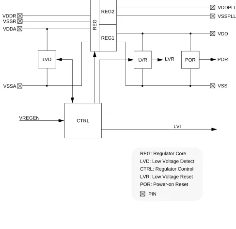
[image:10.612.66.553.187.659.2]1.4 Block Diagram
Figure 1-1shows the function principle of VREG_3V3 by means of a block diagram. The regulator core
REGconsists of two parallel subblocks,REG1 andREG2, providing two independent output voltages.
Figure 1-1 VREG_3V3 - Block Diagram
LVR LVD POR VDDR VDD LVI POR LVR CTRL VSS VDDPLL VSSPLL VREGEN REG REG2 REG1 PIN VDDA VSSA
Section 2 Signal Description
2.1 Overview
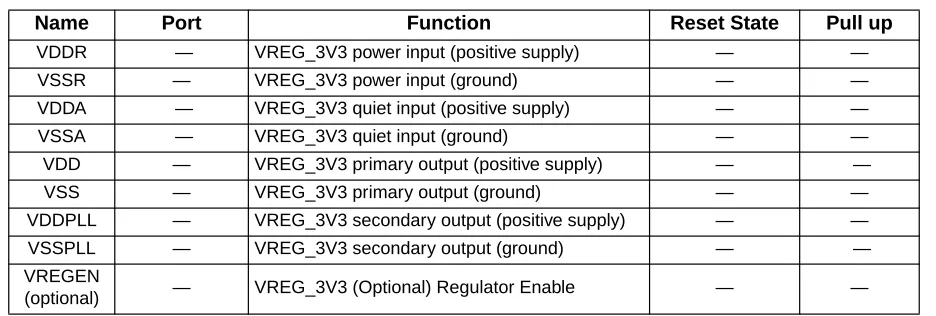
[image:11.612.75.536.209.368.2] [image:11.612.74.542.210.368.2]Due to the nature of VREG_3V3 being a voltage regulator providing the chip internal power supply voltages most signals are power supply signals connected to pads.
Table 2-1 shows all signals of VREG_3V3 associated with pins.
2.2 Detailed Signal Descriptions
Check device level specification for connectivity of the signals.
2.2.1 VDDR, VSSR - Regulator Power Input
Signal VDDR is the power input of VREG_3V3. All currents sourced into the regulator loads flow through this pin. A chip external decoupling capacitor (100nF...220nF, X7R ceramic) between VDDR and VSSR can smoothen ripple on VDDR.
For entering Shutdown Mode pin VDDR should also be tied to ground on devices without VREGEN pin.
2.2.2 VDDA, VSSA - Regulator Reference Supply
Signals VDDA/VSSA which are supposed to be relatively quiet are used to supply the analog parts of the regulator. Internal precision reference circuits are supplied from these signals. A chip external decoupling capacitor (100nF...220nF, X7R ceramic) between VDDA and VSSA can further improve the quality of
Table 2-1 VREG_3V3 - Signal Properties
Name Port Function Reset State Pull up
VDDR — VREG_3V3 power input (positive supply) — —
VSSR — VREG_3V3 power input (ground) — —
VDDA — VREG_3V3 quiet input (positive supply) — —
VSSA — VREG_3V3 quiet input (ground) — —
VDD — VREG_3V3 primary output (positive supply) — —
VSS — VREG_3V3 primary output (ground) — —
VDDPLL — VREG_3V3 secondary output (positive supply) — —
VSSPLL — VREG_3V3 secondary output (ground) — —
VREGEN
12
2.2.3 VDD, VSS - Regulator Output1 (Core Logic)
Signals VDD/VSS are the primary outputs of VREG_3V3 that provide the power supply for the core logic. These signals are connected to device pins to allow external decoupling capacitors (100nF...220nF, X7R ceramic).
In Shutdown Mode an external supply at VDD/VSS can replace the voltage regulator.
2.2.4 VDDPLL, VSSPLL - Regulator Output2 (PLL)
Signals VDDPLL/VSSPLL are the secondary outputs of VREG_3V3 that provide the power supply for the PLL and Oscillator. These signals are connected to device pins to allow external decoupling capacitors (100nF...220nF, X7R ceramic).
In Shutdown Mode an external supply at VDDPLL/VSSPLL can replace the voltage regulator.
2.2.5 VREGEN - Optional Regulator Enable
This optional signal is used to shutdown VREG_3V3. In that case VDD/VSS and VDDPLL/VSSPLL must be provided externally. Shutdown Mode is entered with VREGEN being low. If VREGEN is high, the VREG_3V3 is either in Full Performance Mode or in Reduced Power Mode.
For the connectivity of VREGEN see device specification.
Section 3 Memory Map and Registers
3.1 Overview
This section provides a detailed description of all registers accessible in VREG_3V3.
[image:13.612.111.497.236.282.2]3.2 Module Memory Map
Table 3-1 provides an overview of all used registers.
3.3 Register Descriptions
This section describes in address order all the VREG_3V3 registers and their individual bits.
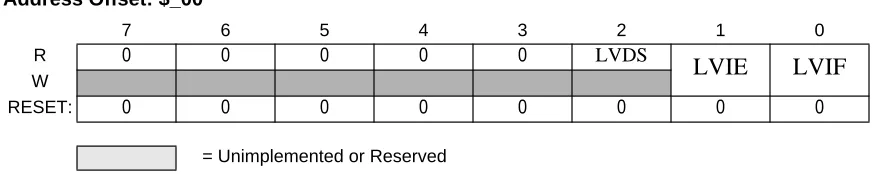
3.3.1 VREG_3V3 - Control Register (VREGCTRL)
[image:13.612.88.527.430.517.2]The VREGCTRL register allows to separately enable features of VREG_3V3.
Figure 3-1 VREG_3V3 - Control Register (VREGCTRL)
LVDS — Low Voltage Detect Status Bit
This read-only status bit reflects the input voltage. Writes have no effect. 1 = Input voltage VDDA is below level VLVIA and FPM.
0 = Input voltage VDDA is above level VLVID or RPM or Shutdown Mode.
Table 3-1 VREG_3V3 - Memory Map
Address
Offset Use Access
$_00 VREG_3V3 Control Register (VREGCTRL) R/W
Address Offset: $_00
7 6 5 4 3 2 1 0
R 0 0 0 0 0 LVDS
LVIE LVIF
W
RESET: 0 0 0 0 0 0 0 0
14
LVIF is set to 1 when LVDS status bit changes. This flag can only be cleared by writing a 1. Writing a 0 has no effect. If enabled (LVIE=1), LVIF causes an interrupt request.
1 = LVDS bit has changed. 0 = No change in LVDS bit .
Section 4 Functional Description
4.1 General
Block VREG_3V3 is a voltage regulator as depicted inFigure 1-1. The regulator functional elements are the regulator core (REG), a low voltage detect module (LVD), a power-on reset module (POR) and a low voltage reset module (LVR). There is also the regulator control block (CTRL) which represents the interface to the digital core logic but also handles the operating modes of VREG_3V3.
4.2 REG - Regulator Core
VREG_3V3, respectively its regulator core has two parallel, independent regulation loops (REG1 and REG2) that differ only in the amount of current that can be sourced to the connected loads. Therefore only REG1, providing the supply at VDD/VSS, is explained. The principle is also valid for REG2.
The regulator is a linear series regulator with a bandgap reference in its Full Performance Mode and a voltage clamp in Reduced Power Mode. All load currents flow from input VDDR to VSS or VSSPLL, the reference circuits are connected to VDDA and VSSA.
4.2.1 Full Performance Mode
In Full Performance Mode a fraction of the output voltage (VDD) and the bandgap reference voltage are fed to an operational amplifier. The amplified input voltage difference controls the gate of an output driver which basically is a large NMOS transistor connected to the output.
4.2.2 Reduced Power Mode
In Reduced Power Mode the driver gate is connected to a buffered fraction of the input voltage(VDDR). The operational amplifier and the bandgap are disabled to reduce power consumption.
4.3 LVD - Low Voltage Detect
Subblock LVD is responsible for generating the low voltage interrupt (LVI). LVD monitors the input voltage (VDDA-VSSA) and continuously updates the status flag LVDS.
Interrupt flag LVIF is set whenever status flag LVDS changes its value.
The LVD is available in FPM and is inactive in Reduced Power Mode and Shutdown Mode.
16
4.5 LVR - Low Voltage Reset
Block LVR monitors the primary output voltage VDD. If it drops below the assertion level (VLVRA) signal LVR asserts and when rising above the deassertion level (VLVRD) signal LVR negates again. The LVR function is available only in Full Performance Mode.
4.6 CTRL - Regulator Control
Section 5 Resets
5.1 General
This section describes how VREG_3V3 controls the reset of the MCU.The reset values of registers and signals are provided in Section 3 Memory Map and Registers. Possible reset sources are listed inTable 5-1.
5.2 Description of Reset Operation
5.2.1 Power-On Reset
During chip power-up the digital core may not work if its supply voltage VDD is below the POR
deassertion level (VPORD). Therefore signal POR which forces the other blocks of the device into reset is kept high until VDD exceeds VPORD. Then POR becomes low and the reset generator of the device continues the start-up sequence. The power-on reset is active in all operation modes of VREG_3V3.
5.2.2 Low Voltage Reset
For details on low voltage reset see section 4.5 LVR - Low Voltage Reset.
Table 5-1 VREG_3V3 - Reset Sources
Reset Source Local Enable
Power-on Reset always active Low Voltage Reset available only in Full
Section 6 Interrupts
6.1 General
This section describes all interrupts originated by VREG_3V3.
The interrupt vectors requested by VREG_3V3 are listed inTable 6-1. Vector addresses and interrupt priorities are defined at MCU level.
6.2 Description of Interrupt Operation
6.2.1 LVI - Low Voltage Interrupt
In FPM VREG_3V3 monitors the input voltage VDDA. Whenever VDDA drops below level VLVIA the status bit LVDS is set to 1. Vice versa, LVDS is reset to 0 when VDDA rises above level VLVID. An interrupt, indicated by flag LVIF=1, is triggered by any change of the status bit LVDS if interrupt enable bit LVIE=1.
NOTE: On entering the Reduced Power Mode the LVIF is not cleared by the VREG_3V3.
Table 6-1 VREG_3V3 - Interrupt Vectors
Interrupt Source Local Enable
Low Voltage Interrupt (LVI)
LVIE=1; available only in Full
24