ISSN Online: 2153-1293 ISSN Print: 2153-1285
DOI: 10.4236/cs.2018.99014 Sep. 17, 2018 133 Circuits and Systems
CM-Biquad Filter Using Single DO-VDBA
Chandra Ketu Yadav, Dinesh Prasad
*, Zainab Haseeb, Laxya, Mayank Kumar
Department of Electronics and Communication Engineering, Faculty of Engineering and Technology, Jamia Millia Islamia, New Delhi, India
Abstract
In this manuscript we present a current mode biquad using one dual out-put-voltage differencing buffered amplifier (DO-VDBA) and four passive components (2 grounded capacitors and 2 resistors). The proposed circuit offers very low active and passive sensitivity. The filter presented here is elec-tronically tunable, frequency of oscillation (FO) can be tuned by controlling transconductance (gm) by varying the bias current (IB) of the circuit. The
workability of proposed circuit is tested using PSPICE with 180 nm TSMC CMOS process parameters.
Keywords
Current Mode, Biquad Filter, Dual Output-Voltage Differencing Buffered Amplifier
1. Introduction
Biquads are the major components in the area of electronics. It is extensively used in numerous electronic applications, which include analog and digital sig-nal processing, communication etc. [1]. Looking at the vast literature available, we are well aware that innumerable filters have been designed till date using several active building blocks and each of them has some advantages and disad-vantages too. Current mode filters have proven its vitality in several aspects, some of them are high performance, lower power consumption, miniaturization of circuit, higher frequency range, increased slew rate and linearity. So in this paper the current mode is exploited to get such benefits. Filters available in lite-rature have also reportedly suffered few problems such as smaller frequency range, lack of tunability and excessive use of passive components.
The filter proposed in this paper uses current mode VDBA, it is single input and dual output and it is electronically tunable as well [2].
FB-VDBA is well known for voltage-mode analog signal processing. It is a How to cite this paper: Yadav, C.K.,
Pra-sad, D., Haseeb, Z., Laxya and Kumar, M. (2018) CM-Biquad Filter Using Single DO-VDBA. Circuits and Systems, 9, 133-139. https://doi.org/10.4236/cs.2018.99014
Received: August 21, 2018 Accepted: September 14, 2018 Published: September 17, 2018
Copyright © 2018 by authors and Scientific Research Publishing Inc. This work is licensed under the Creative Commons Attribution International License (CC BY 4.0).
DOI: 10.4236/cs.2018.99014 134 Circuits and Systems terature [5].
Single VDIBA and a capacitor, can be used to realize a novel voltage-mode (VM) resistorless, 1st-order all-pass filter (APF) [6].
Several analog signal-processing filters are also available using current mode circuit; CDBA is one such ABB [7].
CM filters have proven its vitality in several aspects, some of them are high performance, lower power consumption, miniaturization of circuit, higher fre-quency range, increased slew rate and linearity, so in this manuscript the CM is exploited to get such benefits. Filters available in literature have also reportedly suffered few problems such as smaller frequency range, lack of tunability and excessive use of passive components. FB-VDBA is very useful building block for analog circuit design. It is also helpful in the designing of circuit with least number of passive components [8].
Voltage mode configuration has also been proved helpful in design of a cur-rent-mode and voltage-mode electronically tunable quadrature oscillator that consists of both voltage and current output [9].
To the best awareness of the authors no same type of current mode biquad is available in the open literature. So, in this manuscript we have proposed a bi-quad using single DO-VDBA whose frequency is electronically controllable. Of-fering very low active and passive sensitivities are also important characteristics of this circuit.
2. The Proposed New Structure
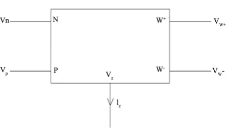
The DO-VDBA is represented in its symbolic form as shown in Figure 1, where the input terminals are given by P and N while the output terminals are denoted by z, w+ and w−. Current flowing through “z” terminal is given by the difference
of VP and VN by transconductance (gm). The VW is same as the VZ. The electronic
controllability of DO-VDBA has advantages over the traditional VDBA by pos-sibility of controlling of gmthrough the bias current IB.
The DO-VDBA can be given by the following matrix:
0 0 0
0 0 0
0
0 0 1
0 0 1
p
n p
z m m n
w z
w
I
I V
I g g V
V V
V
+
−
= −
−
DOI: 10.4236/cs.2018.99014 135 Circuits and Systems Figure 1. Symbolic notation of the DO-VDBA.
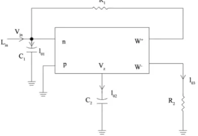
After applying KCL at different nodes of Figure 2 the proposed structure yields the following current transfer functions:
( )
1 21
2
1 1 1 1 2
C
m in HPF
I s
T s g
s
I s
R C R C C
= =
+ + (2)
( )
2 12
2
1 1 1 1 2
m C m in BPF sg C I
T s s g
I s
R C R C C
−
= =
+ + (3)
( )
2 2 1 23
2
1 1 1 1 2
m
R
m in LPF
g R C C I
T s s g
I s
R C R C C
= =
+ + (4)
( )
2
4 1 2 1 2
4
2
1 1 1 1 2
m m
m in APF
sg g
s
I C R C C
T s s g
I s
R C R C C
− +
= =
+ + (5)
where I4=Ic1+Ic2+Ir2
( )
2
5 2 1 2
5
2
1 1 1 1 2
m
m in BRF
g s
I R C C
T s g
s
I s
R C R C C
+
= =
+ + (6)
where I5=Ic1+Ir2.
The cutoff frequency ω0, bandwidth (BW) and quality factor Q0 are given by:
0
1 1 2 m
g R C C
ω
= (7)0
0 1 1
1 B Q C W R ω =
= (8)
1 1 0
2 m
g R C Q
C
DOI: 10.4236/cs.2018.99014 136 Circuits and Systems Figure 2. The proposed configuration.
3. Sensitivity Analysis
The various sensitivities of ω0 and Q0 w.r.t. each passive and active element are:
Sensitivity of y with respect to x is symbolized as y
x y y x y
S
x x y x
∂ ∂
= ∂ =
∂
It’s active and passive sensitivity of circuit analysis parameter are expressed as:
1)
0 0 0 0 1 1 2
0 1 1 2
1 1 2
1 1 2
1 1 1 1
2 2
m
m
m m
g
m m m m m
m
m m
g R C C
g g
S
g g g g g R C C
g R C C
g R C C g
ω ω ω ω
ω ∂ ∂ ∂ = = ∂ ∂ ∂ = = = 2) 0 2 2 2
0 0 2 0 1 1
2 2 0 2 1 1 2 2
2 2 1 1
3
1 1 2
1 1 1
2 2 Q m C m m m C C
Q Q C Q g R C
S
C C Q C g R C C C
C C g R C
g R C C
∂ ∂ ∂ = = ∂ ∂ ∂ − − = = = 3) 0 1
1 1 1 2
0 0 1 0
1 1 0 1 1 1 1 2
1 1 1 2
3
1 2 1
1 1 1
2 2 m R m m m
R R C C g
R S
R R R g R R C C
g R R C C
g C C R
ω ω ω ω
ω ∂ ∂ ∂ = = ∂ ∂ ∂ − − = = = 4) 0 1
1 1 1 2
0 0 1 0
1 1 0 1 1 1 1 2
1 1 1 2
3
1 2 1
1 1 1
2 2 m C m m m
C R C C g
C S
C C C g C R C C
g C R C C
g R C C
ω ω ω ω
ω ∂ ∂ ∂ = = ∂ ∂ ∂ − − = = = 5) 0 2
2 1 1 2
0 0 2 0
2 2 0 2 2 1 1 2
2 1 1 2
3
1 1 2
1 1 1
2 2 m C m m m
C R C C g
C S
C C C g C R C C
C R C C g
R C
g C
ω ω ω ω
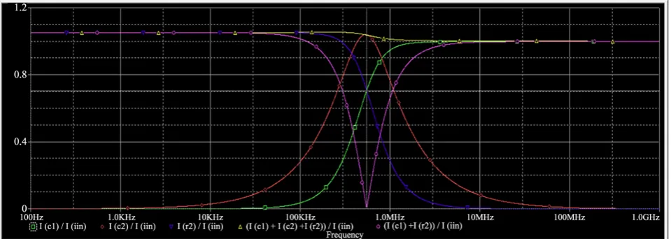
DOI: 10.4236/cs.2018.99014 137 Circuits and Systems Figure 3. Frequency response of the proposed biquad.
6)
0 0 0 0 2 1 1
0 1 1 2
2 1 1
2 1 1
1 1 1
2 2
m
m
Q m m
g
m m m m m
m
m m
g C
Q Q g Q g R C
S
g g Q g g R C g C
g C R C
C
g R C g
∂ ∂ ∂
= =
∂ ∂ ∂
= =
=
7) 0 1
1 2
0 0 1 0 1 1
1 1 0 1 1 1 1 2
1 2 1
2
1 1 1
1 1 1
2 2
Q m
R
m
m
m
R C
Q Q R Q g R C
S
R R Q R g R C R C
R C g C
C
g R C R
∂ ∂ ∂
= =
∂ ∂ ∂
= =
=
8) 0 1
1 2
0 0 1 0 1 1
1 1 0 1 1 1 1 2
1 2 1
2
1 1 1
1 1 1
2 2
Q m
C
m
m
m
C C
Q Q C Q g R C
S
C C Q C g R C C C
C C g R
C
g R C C
∂ ∂ ∂
= =
∂ ∂ ∂
= =
=
From above values of sensitivity, concluding the values here:
0 0 0 0
1 1 2, , , ,1 1, , 2
1, 1 1 1
2 2 2 2
m m
Q Q
g R C C g R C C
Sω = Sω = − S = S = − (10)
From Equation (10) it is clear that the proposed circuit offers small active and passive sensitivities.
4. Simulation Result
To show the functionality the presented biquad is tested using SPICE simula-tions. For this purpose we use CMOS DO-VDBA [5] with power supply voltage taken as VDD = −VSS = 1.2 V, Ib = 50 μA biasing current and passive elements
with C1 = 0.1 nF, C2 = 0.2 nF, R1 = 2 kΩ and R2 = 2 kΩ. The frequency response
of the circuit is depicted in Figure 3 with the cutoff frequency f0 = 0.78 MHz.
5. Conclusion
DOI: 10.4236/cs.2018.99014 138 Circuits and Systems
Acknowledgements
This research is supported by the “Young Faculty Research Fellowship and Research/Contingency Grant”, under the “Visvesvaraya PhD Scheme for Elec-tronics and IT”, Ministry of ElecElec-tronics and Information Technology, Govt. of India.
Conflicts of Interest
The authors declare no conflicts of interest regarding the publication of this pa-per.
References
[1] Toumazou, C., Lidgey, F.J. and Haigh, D.G. (1992) Analogue IC Design: The Cur-rent Mode Approach. IEE Circuits and Systems Series: Institution of Electrical En-gineers. IET, Stevenage.
[2] Biolek, D., biolkova, V. and Kolka, Z. (2010) All Pass Filter Employing Fully Ba-lanced Voltage Differencing Buffered Amplifier. Proceeding of IEEE Latin Ameri-can Symposium Circuits and Systems, Foz do Iguacu, 24-26 February 2010, 232-235. [3] Biolkova, V., Kolka, Z. and Biolek, D. (2009) Fully Balanced Voltage Differencing
Buffered Amplifier and Its Application. 2009 52nd IEEE International Midwest Symposium on Circuits and System, Cancun, 2-5 August 2009, 45-48.
https://doi.org/10.1109/MWSCAS.2009.5236157
[4] Kacar, F., Yesil, A. and Noori, A. (2012) New CMOS Realization of Voltage Diffe-rencing Buffered Amplifier and Its Biquad Filter Applications. Radio Engineering, 21, 333-339.
[5] Sotner, R., Jerabek, J. and Herencsar, N. (2013) Voltage Differencing Buffered/Inverted Amplifiers and Their Applications for Signal Generation. Radio Engineering, 22, 490-504.
[6] Acar, C. and Ozogue, S. (1999) A New Versatile Building Block: Current Differenc-ing Buffered Amplifier. Microelectronics Journal, 30, 157-160.
https://doi.org/10.1016/S0026-2692(98)00102-5
[7] Herencsar, N., Minaei, S., Koton, J., Yuce, E. and Vrba, K. (2013) New Realization of Dual-Output Voltage Mode All Pass Filtering Using Voltage Differencing Inve-reted Buffered Amplifier. Analog Integrated Circuits and Signal Processing, 74, 141-154. https://doi.org/10.1007/s10470-012-9936-2
DOI: 10.4236/cs.2018.99014 139 Circuits and Systems https://doi.org/10.1515/jee-2016-0019
[9] Yesil, A. and Kacar, F. (2018) Current and Voltage Mode Quadrature Oscillator Based on Voltage Differencing Buffered Amplifier. Electrical, 18, 6-12.