Structural and Optical Dispersion Characterisation of
Sprayed Nickel Oxide Thin Films
Safwat A. Mahmoud1*, Shereen Alshomer1,2, Mou’ad A. Tarawnh3
1Physics Department, Faculty of Science, University of Hail, Hail, Kingdom of Saudi Arabia 2The National University of Malaysia, Bangi, Malaysia
3School of Applied Physics, Faculty of Science and Technology, The National University of Malaysia, Banji, Malaysia
E-mail:*samahmoud2002@yahoo.com
Received January 24, 2011; revised June 10, 2011; accepted June 23, 2011
Abstract
Crystalline and non-crystalline nickel oxide (NiO) thin films were obtained by spray pyrolysis technique (SPT) using nickel acetate tetrahydrate solutions onto glass substrates at different temperatures from 225 to 350˚C. Structure of the as-deposited NiO thin films have been examined by X-ray diffraction (XRD) and atomic force microscope (AFM). The results showed that an amorphous structure of the films at low sub-strate temperature (Ts = 225˚C), while at higher Ts ≥ 275˚C, a cubic single phase structure of NiO film is
formed. The refractive index (n) and the extinction coefficient (k) have been calculated from the corrected transmittance and reflectance measurements over the spectral range from 250 to 2400 nm. Some of the opti-cal absorption parameters, such as optiopti-cal dispersion energies, Eo and Ed, dielectric constant, ε, the average
values of oscillator strength, So, wavelength of single oscillator λo and plasma frequency, ωp, have been
eva-luated.
Keywords:Nickel Oxide Thin Films, Nickel Acetate, Optical Dispersion, Spray Pyrolysis Technique, AFM, XRD
1. Introduction
The optical properties of thin films are very important for many applications, including interference devices, such as antireflection coatings, laser mirrors and monochro-matic filters, as well as optoelectronics, integrated optics, solar power engineering, microelectronics and optical sensor technology depending on the reflectance and transmittance properties of the films during their prepa-ration.
Dispersion models parameterize the spectral depend-encies on the dielectric functions of films or correspond-ing functions, such the band gap, optical dispersion ener-gies, Eo, Ed, dielectric constant, ε, ratio between the
number of charge carriers and the effective mass, N/m*, wavelength of the single oscillator, λo, plasma
fre-quency…etc., can be determined by data treatment. The optical constants of thin films provide us with informa-tion concerning with microscopic characteristics of the material.
Transition metal oxides like nickel oxides have found
wide applications due to these anti-ferromagnetic semi-conductor with wide gab≈ 3.6 eV and cubic rock salt- like crystal structure [1,2]. It offers promising candida-ture for many application such as electrocatalysis [3], positive electrode in batteries [4], fuel cell [5], electro-chromic devices [6], solar thermal absorber [7], catalyst for oxygen evolution [8] and photo electrolysis [9]. Sev-eral physical and chemical methods, such as sputtering [10], pulsed laser deposition [11], chemical bath deposi-tion [10,12] and sol-gel [13] have been used to obtain nickel oxide films. All these methods offer different ad-vantages depending on the application of interest and many efforts have been conduced to obtain films with the desirable physical and/or chemical properties. Among the different methods for film deposition, the relative simplicity of the spray pyrolysis method and its potential application for large area deposition make it very attrac-tive, low cost and feasible for mass production processes.
tech-nique (SPT) using nickel acetate tetrahydrate solutions onto glass substrates. The accurate determination of the optical constants of these materials is important, not only in order to know the basic mechanisms underlying these phenomena, but also to exploit and develop their interest-ing technological applications. Therefore, the optical absorption parameters, such as optical dispersion ener-gies, Eo, and Ed, dielectric constant, ε, the average values
of oscillator strength So, wavelength of single oscillator λo, and plasma frequency, ωp, have been evaluated under
the effect of substrate temperature.
2. Experimental Details
2.1. Film Preparation
Nickel acetate tetrahydrate (Ni(C2H3O2)2·4H2O) in a concentration of 5 × 10⁻² M in ethanol was used as a starting solution for deposition of nickel oxide films. Nickel acetate tetrahydrate decomposes in a two step- process, firstly dehydration from 95˚C to 150˚C and se-condly decomposition of the acetate between 300˚C to 350˚C [14,15]. The solution was passed through a pneu-matic nebulizer with a nozzle diameter of 0.7 mm. The spraying process lasted for about 15 s. The period be-tween spraying processes was about 3 min; this period is enough to avoid excessive cooling of glass substrate. The overall reaction process can be expressed as heat de-composition of nickel acetate to clusters of nickel oxide in the presence of water and air oxygen.
In order to explore the influence of the ultrasonically cleaned preheated glass substrate temperature (Ts), dif-ferent deposition temperatures ranged between 225 to 350˚C were used to prepare these films. In order to get uniform thin films, the height of spraying nozzle, solu-tion molarity and the rate of spray process were kept constant during the deposition process at 35 cm, 5 × 10⁻² M and 15 cm3/min, respectively. A thermocouple was fixed to the substrate surface using silver past and the temperature was measured at the four corners of the glass substrate surface, then the results were averaged and the standard deviation was calculated (± 5˚C).
2.2. Thickness Measurements
Thickness of the as-deposited films prepared at different substrate temperatures was determined by multiple-beam Fizeau fringes at reflection using either white light or monochromatic light (Hg, λg = 546 nm). A glass sub-strate was partially masked during deposition of the film to obtain a sharp edge. Then, a thermally evaporated aluminum layer coated the total surface of the substrate. The colored interference fringes enabled the
determina-tion of the order of magnitude of the fringes shift, while the monochromatic fringe shift, as a fraction of the order separation was measured using an eyepiece micrometer.
2.3. Structural Investigation
Crystallinity and the phases of the as-deposited films were characterized using JEOL X-ray diffractometer (XRD) (Model JSDX-60PA) with monochromatic high- intensity Cu Kα radiation (λ = 0.154184 nm). Continuous scanning was applied with a slow scanning speed (1˚/min) and a small time constant (1 s).
2.4. Microstructure Analysis
Atomic force microscope (AFM) was used to analyze microstructures by molecular imaging in two- and three-dimensions. The atomic cross-section and surface roughness were determined. Each sample before AFM investigation was washed carefully with distilled water and dried. A Nanoscope III instrument with a 100 μm long silicon tip with repulsive and constant interaction force less than a few nano-Newtons were used [16].
2.5. Optical Measurements
Optical transmission and reflection of the prepared films were recorded over the wavelength range from 250 - 2400 nm using Shimadzu UV 3101 PC; UV-Vis-NIR double-beam spectrophotometer with reflection attach-ment based on V-N geometry (incident angle 5˚). The spectral variation of transmission and reflection obtained in this work are used to provide a qualitative guide to the film quality. A laboratory developed computer program [16] was used to calculate the absorption coefficient, energy gaps, optical constants and dielectric constants.
3. Results and discussion
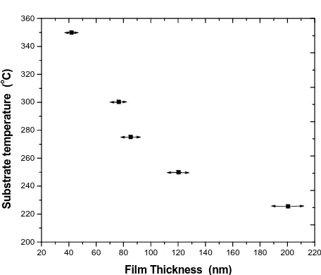
3.1. Variation of the Film Thicknesses with Substrate Temperature
20 40 60 80 100 120 140 160 180 200 220 200
220 240 260 280 300 320 340 360
Film Thickness (nm)
Subst
rat
e t
e
m
p
e
rat
ur
e (
[image:3.595.58.286.70.265.2]o C)
Figure 1. Variation of film thicknesses with substrate tem-peratures.
higher temperatures. In addition, the decrease in the film thickness may be attributed to water loss [17] or removal of interlayer water with consequent formation of com-pact NiO films.
[image:3.595.57.287.508.692.2]3.2. Structural Characterization
Figure 2 shows the variation of the diffraction patterns as a function of the substrate temperature. The Bragg geometry is employed for analysis and the results of XRD for the as-deposited NiO films at Ts = 225˚C – 250˚C show that the film structure is non-crystalline structure. Further increasing in the substrate temperature up to ≥ 275˚C, the films were fully transformed to poly-crystalline phase of NiO (JCPDS 47-1049) with cubic structural [9,18,19].
10 20 30 40 50 60
(220)
(2
00)
(1
11
)
350 oC
300 o C
275 oC
250 o C
225 oC
X
R
D
i
n
te
n
s
ity
(a
. u
.)
2
Figure 2. The X-ray diffractograms of NiO films at differ-ent substrate temperatures.
Three peaks are observed in the pattern at 2θ = 37.1˚, 43.3˚ and 62.8˚ assigned to the (111), (200) and (220) crystal planes, respectively. The estimated lattice pa-rameters was found to be a = b = c = 0.417 nm. The in-crease in the amount and degree of crystallinity of the phase is indicated by the enhancement of the peak inten-sity. Furthermore, no other peaks corresponding to other phases have emerged. This suggested that, NiO phase is stable and its formation is independent of substrate tem-perature. The films show prefential growth along the [111] direction. The increase in the intensity of the peaks may be attributed to the increase in the degree of crystal-linity caused by increasing the substrate temperature.
Scherre’s formula on the bases of full-wave at Half- Maximum (FWHM) was used to calculate the grain size and the average grain size was found to increase from 38 to 45 nm with increasing the substrate temperature from 275˚C to 350˚C.
3.3. Microstructural Characterization
Figure 3 shows a NiO crystal surface imaged with the AFM in air and the three-dimensional plot (Figure3(a)) atomic corrugations are visible as well as grains can be seen on the thin film (Figure3(b)). The relative smooth surface could be seen with 45 nm thick. A grain size analysis of the thicker NiO film gives a mean grain size area of 3.9 μm2. This means that an average radius of the grains of ≈ 35 nm could be determined. These data are found to be in a good agreement with XRD measure-ments.
The roughness analysis and the cross section profile shown in Figure 3(c) give an impressive insight of the excellent capability of the method to measure surface topography. The surface roughness, (R) is the mean roughness of the surface relative to the center plane of the glass substrate ranged between 0.5 and 1.5 nm. However, the thicker film was found to have a greater roughness than that of the thinner one.
3.4. Optical Characterization
Optical measurements of transmittance and reflectance of the films deposited at different substrate temperatures are shown in Figure4. These measurements have been taken in the wavelength range from 250 to 2400 nm. The optical properties of the investigated films were studied by the method of the spectral optical absorption and re-flection. The spectral data of normal transmittance, Texp
(λ), and reflectance, Rexp(λ), were corrected due to
sub-strate effect according to the following formula [20].
2
2 2
1exp sub exp sub
sub exp exp
T T R R
T =
T T R
Figure 3. Three-dimensional AFM images of atomic resolution of NiO films (a), AFM images with total number of grains, mean and standerd deviation of of defined grains (b), with corresponding atomic cross-section analysis of NiO thin films (c).
Figure 4. The transmittance spectrum of NiO films pre-pared at different substrate temperature.
2 2 2 22exp sub exp sub sub exp sub
R T T R
R =
T T R
(2)
where Tsub and Rsub are the transmittance and the
reflec-tance of the glass substrate respectively. As shown in Figure 4, the general increase in the transmittance is observed as the film thickness decrease. This behavior may be attributed to perfection and stoichiometry of the films.
Anomalous behaviour is observed at low substrate temperature that disappearing in the absorption edge and
lowering in the transmittance. This probably is due to the following reasons.
1) Transformation of the phase from amorphous to crystalline considering the sample prepared at Ts = 250˚C as a critical case.
2) Absorption edge disappeared in the films that de-posited in low temperature; this is due to the fact that, as Ts decreases, bigger clusters are formed before the film creation and the scattered radiation became remarkable due to the surface roughness.
3) Adsorption of water in films deposited at low tem-peratures during the handling of the film.
3.4.1. Optical Energy Gap
From the transmittance data and according to Tauc [21] relation, (αE)2 versus incident photon energy, (E), plots were obtained. The graphs are represented in Figure5. The band gap energy values are found to be 3.83 and 3.14 eV for the NiO thin films with increasing the sub-strate temperature from 225˚C to 350˚C, which are in a good agreement with that obtained for normal bulk NiO (3.6 - 4.0 eV) [22].
Figure 5. The (αhν)2 vs. hν plot for NiO thin films at
differ-ent substrate temperature.
3.4.2. Determination of Refractive Index
Refractive index is one of the fundamental properties for an optical material because it is closely related to the electronic polarization of ions and the local field inside materials. The complex optical constant (refractive in-dex, (n)) of the prepared samples has been calculated from the corrected T(λ) and R(λ) using a developed com-putation program [24].
2
2 1 1 n
R =
n
and
2 41 n
T =
n
(3)
where n is the refractive index of the thin film. The re-flectance, R, at the vacuum-film interface has to take into consideration with the value of extinction coefficient, k, so that R can be written as Karmers-Kronig relation.
2 2
2 2 1 1
n + k
R
n + k
(4)
The behaviour of refractive index has a higher value at very low wavelength (strong absorption). This is due to the quality between the frequency of incident electro-magnetic radiation and the plasma frequency. Therefore, there is an anomalous dispersion of refractive index in the region of the plasma frequency. But when λ crosses λp (plasma wavelength) and the corresponding dielectric constant becomes negative, the refractive index becomes largely imaginary. Hence, there is no propagation of electromagnetic radiation through the medium and gets reflection as mentioned before.
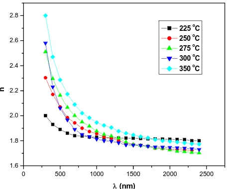
Figure 6 shows the spectral variation of the refractive
0 500 1000 1500 2000 2500
1.6 1.8 2.0 2.2 2.4 2.6 2.8
n
(nm)
225 oC 250 oC 275 o
C 300 o
C 350 oC
Figure 6. The refractive index (n) of NiO films as a function of wavelength λ, at different substrate temperatures.
index as a function of wavelength at different substrate temperatures. It can be seen that, the maximum value of refractive index (n = 2.8 at Ts = 350˚C) at very low wa-velength, λ = 300 nm (strong-absorption region), was observed in all samples. This is due to the equality be-tween the frequency of incident electromagnetic radia-tion and the frequency of electrons. This leads to the coupling of electrons in NiO films to the oscillating elec-tric field. At longer wavelengths, λ > 500 nm, the refrac-tive index is sharply decreasing for all patterns reaching to the lowest value of 1.8 at λ ≥ 900 nm and then the n value remains slightly changed for the whole wavelength. Furthermore, the behaviors of refractive index of all films are similar, which is due to the normal dispersion. In the NIR region, λ ≥ 1000 nm, the n values differ slightly with substrate temperature, which diverge re-markably in the visible region. These results are in good agreement with the data obtained by others [9] in the same phase.
3.4.3. Determination of Dielectric Constant
Analyses of the obtained data of refractive index can be used to obtain the high frequency dielectric constant through two procedures [25]: The first, describes the contribution of the free carriers and lattice vibration modes of the dispersion, while the second procedure is based upon the dispersion arising from the bound carriers in an empty lattice. However, both procedures were em-ployed for the obtained value of lattice high frequency dielectric constant ε.
3.4.3.1. The First Procedure
[image:5.595.310.538.77.267.2]index [26]:
2 2
(1)
4π
2
2 *
o
e N
n
c m
(5)
as shown in Figure7, at λ and n = 0, the values of ε and
ωp are listed in Table 1.
3.4.3.2. The Second Procedure
Determination of the dielectric constant could be defined using the dispersion relation of the incident photon. The refractive index was also fitted using a function for ex-trapolation towards shorter wavelength. The Moss model [32], which stated that: “the free carriers contribution to dispersion are relatively small”. This means that data corresponding to the wavelength range lying below the absorption edge of the material has to be used [33]. The properties of the investigated NiO could be treated as a single oscillator at wavelength λo at high frequency. The following equation which calculates the high frequency dielectric constant ε(2) is:
where c is the velocity of the light, εo the permittivity of free space (8.854 × 10⁻¹² F/m), N the free carrier concen-tration and m* the effective mass of the charge carriers. The nature of the dispersion of n2 as a function of wave-length (λ2) for different substrate temperatures is shown in Figure7. As shown un this Figure, the refractive in-dex is an anomalous dispersion in the region of the high frequency. Both the refractive index and increases and absorption of electromagnetic radiation were found to be increased as frequency increases. Furthermore, the re-fractive index becomes largely, when the frequency of the radiation crosses with the characteristic frequency of the electron. Hence, there is no propagation of electro-magnetic radiation through the NiO films. From Figure 7, it can be seen that the dependence of n2 is linear at longer wavelength. The values of lattice high frequency dielectric constant, ε(1),is determined from the
intersec-tion of the straight line with λ2 = 0. The values of ε
(1)
increased with increasing substrate temperature (subfig-ure). Table 1 shows the values of both ε(1) and the ratio,
N/m*, of the investigated films at different substrate tem-peratures, which determined from the intercept and slopes of the line, respectively. The obtained values of the ration N/m* were in the range between 6.25 × 1040 to 5.49 × 1040 cm–3g–1 with different substrate temperatures. These results are in a good agreement with Al-Ghamdi et al. [19] for NiO thin films and Hutchines et al. [27] and El-Nahass et al. [28] found (N/m*) for WO3, nickel phthalocyanine films, and also for TiInS2 single crystal [29], in the same order. It is known that in the range of transparency, when the electron damping parameter
,
2 2
2 1
1
o o o
S
n
(7)
where So is the average oscillator strength and λo an
aver-age oscillator wavelength. Equation (7) can be written in the following former:
2 2
2 1
1 1
o
n = n
(8)
2
2 p
2
n
n2 (6)
where ωp is the plasma frequency and 2pe N2 om*,
and ω the incident light frequency [30,31]. From the ap-proximation of the linear part of the dependences n2(λ2)
[image:6.595.312.537.352.583.2]of NiO films deposited at different substrate temperatures, Figure 7. The relation between n2 and λ2 for NiO films.
Table 1. Dispersionparameters of NiO thin film prepared at different substrate temperature.
εL
Ts
(˚C) ε∞(1)
(±4 × 10⁻³) (±6 × 10ε∞(2) –3)
N/m* (cm–3g–1) (±3 × 10⁻²)
λo (nm)
(±2 )
So (m)–2
(±4 × 10⁻⁴) (±4 × 10ωp (Hz) –3) Ed (eV) Eo (eV) Eg (eV) Eo/Eg M–1 M–3
[image:6.595.57.540.629.719.2]
1
[image:7.595.310.537.79.262.2]where n is the refractive index at infinite wavelength. Table 1 shows the values of λo and So values were
ob-tained from slope and intercept of (n21) versus 2 curves at different substrate temperatures. The intersec-tion with (n21)1 axis is (n2 1)1and hence, n2 at λo
equal to ε. Figure 8 shows the variation between and
2
(n 1)1 2 at different substrate temperatures from 225˚C to 350˚C. In addition, the values of the high frequency dielectric constant ε(2) increased with an in-creasing in the substrate temperature. The values of ε(1) and ε(2) are shown in insert graph and tabulated in Table 1. The values of ε(1) and ε(2) are closed with each other and small difference between them may be due to the lattice vibrations and bounded carriers in an empty lattice which are in the transparent region [34,35]. The differ-ence between ε(1) and ε(2) decreased with increasing substrate temperature. This means that the lattice vibra-tion and bounded currieries decreased with increasing the of substrate temperature.
Moreover, the values of average oscillator strength (So)
were calculated from Figure 8. These values are in a good agreement with that obtained by Assim for TiO films [33], byAbdel-Aziz et al. forGeSe(9–x)Tlx thin-film
[36] and also, by Caglar et al. for sulfonated poly-aniline film (SPAN) [34]. Unfortunately, there are no data about high frequency dielectric constant of NiO thin films were found to compare.
3.4.4. Dispersion Energy Parameters of NiO Thin Films
The dispersion energy plays an important role in the re-search for optical materials because it is a significant factor in optical communication and in designing devices for spectral dispersion. The dispersion of refractive index in NiO films was analyzed using the concept of the sin-gle oscillator and can be expressed by Wemple and Di-Domenico relationship [35]:
2
2 2
1 d o
o E E n
E E
(9) where E, Eo and Ed are the photon energy, the oscillator
energy and the dispersion energy, respectively. The pa-rameter Ed, which is the measure of the intensity of the
inter-band optical transition, does not depend signifi-cantly on the band gap. A plot of versus E2 of NiO deposited films for different substrate temperatures as shown in Figure 9. It is clear that, the effect of sub-strate temperature on the refractive index and semicon-ductor dispersion profiles were exhibited a linear dis-placement in the shape of the dispersion profile with de-creasing refractive index. The refractive index declines towards long wavelengths. This is due to the influence of lattice absorption. The values of Ed and Eo were obtained
[image:7.595.310.539.313.501.2]2 (n 1)
Figure 8. The (n2–1)–1 as a function of reciprocal function of
square wavelength for NiO films at different substrate temperature.
Figure 9. The (n2–1)–1 as a function of reciprocal function of
square photon energy for NiO films at different substrate temperature.
from the slope and the intercept, respectively, resulting from the extrapolation of the lines. The individual errors in the calculated Eoand Ed should be significantly small
to make the proposed method significant. The values of the standard deviation of the parameters Eoand Ed
pre-sented in Table 1 were calculated by the fitting proce-dure. The variation of Eo and Ed with different substrate
temperatures are shown in Figure 9. The values of Eo
ergy gap d g E E
was given by relation of Tanaka [37] as
g . The average ratio
2 d
o
E d
o g
E E for NiO thin films at different substrate temperatures is calculated as 1.87, which shows an agreement with this relation. A simple connection between the single-oscillator parameters of Eo and Ed and the imaginary part of the dielectric
con-stant, ε(2), spectrum can be expressed in terms of mo-ments of the ε (2) as follows [34]:
3
2 1 1
3 3
and
o d2
M M
E = E =
M M
(10)
The oscillator energy Eo, which was independent of
the scale of ε2 is consequently an ‘‘average’’ energy gap, whereas Ed depends on the scale of ε2 and thus serves as
an inter band strength parameter. Since the M–1 and M–3 moments are involved in computation of Eo and Ed and
the values of M–1 and M–3 are listed in Table 1.
4. Conclusions
1) Nickel oxide thin films are prepared by spray pyroly-sis technique (SPT) using nickel acetate tetrahydrate so-lutions onto glass substrates at different temperatures ranged from 225˚C to 350˚C.
2) XRD analyses show that an amorphous films have been obtained at low Ts = 225˚C, while at higher Ts ≥ 275˚C a cubic single phase structure of NiO film is formed and the films show prefential growth along the [111] direction.
3) AFM shows relatively smooth surface with 45 nm thick. A grain size analysis of the thicker NiO film gives a mean grain size area of 3.9 μm2.
4) The refractive index for the prepared films depends on the substrate temperature and film thickness. The higher value of the refractive index at very low tempera-ture at λ > 400 nm was observed in all samples.
5) The values of ε∞(1) and ε∞(2), which determined by two different procedures are increased with increasing Ts, while the values of Eo decrease with increasing Ts.
5. References
[1] D. Adler and J. J. Feinleib, “Electrical and Optical Prop-erties of. Narrow-Band Materials,” Physical Review B, Vol. 2, No. 8, 1970, pp. 3112-3134.
doi:10.1103/PhysRevB.2.3112
[2] M. Zöllner, S. Kipp, and K. D. Becker, “Reactive Proc-esses of Nickel Oxide on Oxidic Substrates as Observed by Scanning Force Microscopy,” Crystal Research and Technology, Vol. 35, No. 3, 2000, pp. 299-305.
doi:10.1002/1521-4079(200003)35:3<299::AID-CRAT29 9>3.0.CO;2-I
[3] E. J. M. O’Sullivan and E. J. Calvo, “Reactions at Metal Oxide Electrodes Comprehensive Chemical Kinetics” Elsevier, New York, 1987.
[4] C. M. Lambert and G. Nazri, P. C. Yu, “Spectroscopic and Electrochemical Studies of Electrochromic Hydrated Nickel Oxide Films,” Solar Energy Materials, Vol. 16, 1987, pp. 1-17. doi:10.1016/0165-1633(87)90003-7
[5] N. Shaigan, D.G. Ivey and W. Chen, “Metal-Oxide Scale Interfacial Imperfections and Performance of Stainless Steels Utilized as Interconnects in Solid Oxide Fuel Cells,” Journal of The Electrochemical Society, Vol. 156, No. 6, 2009, pp. B765-B770. doi:10.1149/1.3116252
[6] K.K. Purushothaman and G. Muralidharan, “Nanostruc-tured NiO Based All Solid State Electrochromic Device,” Journal of Sol-Gel Science and Technology, Vol. 46, 2008, pp. 190-197. doi:10.1007/s10971-007-1657-0
[7] R. Cerc Korosec, P. Bukovec, B. Pihlar, A. Surca Vuk, B. Orel and G.Drazic,” Preparation and Structural Investiga-tions of Electrochromic Nanosized NiOx Films Made via the Sol-Gel Route,” Solid State Ionics, Vol. 165, No. 1-4, 2003, pp. 191-200. doi:10.1016/j.ssi.2003.08.032
[8] B. Sasi and K. G. Gopalchandran, “Nanostructured Me-soporous Nickel Oxide Thin Films,” Nanotechnology, Vol. 18, 2007, pp. 115613-115617.
[9] H. Kamel, E. K. Elmaghraby, S. A. Ali and K. Abdel- Hady,” The Electrochromic Behavior of Nickel Oxide Films Sprayed at Different Preparative Conditions,” Thin Solid Films, Vol. 483, No. 1-2, 2005, pp. 330-339.
doi:10.1016/j.tsf.2004.12.022
[10] A. Mendoza-Galván, M. A. Vidales-Hurtado and A. M. López-Beltrán, “Comparison of the Optical and Structural Properties of Nickel Oxide-Based Thin Films Obtained by Chemical Bath and Sputtering,” Thin Solid Films, Vol. 517, No. 10, 2009, pp. 3115-3120.
doi:10.1016/j.tsf.2008.11.094
[11] I. Valyukh, S. Green, H. Arwin, G. A. Niklasson, E. Wäckelgård and C. G. Granqvist, “Spectroscopic Ellip-sometry Characterization of Electrochromic Tungsten Oxide and Nickel Oxide Thin Films Made by Sputter Deposition,” Solar Energy Materials & Solar Cells, Vol. 94, 2010, pp. 724-733.
doi:10.1016/j.solmat.2009.12.011
[12] M.A. Vidales-Hurtado and A. Mendoza-Galv´an, “Opti-cal and Structural Characterization of Nickel Oxide- Based Thin Films Obtained by Chemical Bath Deposi-tion,” Materials Chemistry and Physics, Vol. 107, No. 1, 2008, pp. 33-38.
doi:10.1016/j.matchemphys.2007.06.036
[13] E. Ozkan Zayim, I. Turhan, F.Z. Tepehan and N. Ozer, “Sol-Gel Deposited Nickel Oxide Films for Electrochro-mic Applications,” Solar Energy Materials & Solar Cells, Vol. 92, 2008, pp. 164-196.
doi:10.1016/j.solmat.2007.03.034
[14] J. D. Desai, S.-K. Min, K.-D. Jung and O.-S. Joo, “Spray pyrolytic Synthesis of Large Area NiOx Thin Films from Aqueous Nickel Acetate Solutions,” Applied Surface Sci-ence, Vol. 253, 2006, pp. 1781-1788.
doi:10.1016/j.apsusc.2006.03.009
Pyroly-sis,” Thin Solid Films, Vol. 518, No. 16, 2010, pp. 4499- 4502. doi:10.1016/j.tsf.2009.12.016
[16] A. Richter and R. Ries, “Surface Growth Modes Ana-lysed with Modern Microscopic and Computing Tech-niques,” European Journal of Physics, Vol. 17, 1996, pp. 311-318. doi:10.1088/0143-0807/17/6/002
[17] H. Kamal, E. K. Elmaghraby, S. A. Aly and K. Ab-del-Hady, “Characterization of Nickel Oxide Films De-posited at Different Substrate Temperatures Using Spray Pyrolysis,” Journal of Crystal Growth, Vol. 262, No. 1-4, 2004, pp. 424-434.
doi:10.1016/j.jcrysgro.2003.10.090
[18] A. A. Al-Ghamdi, W. E. Mahmoud, S. J. Yaghmour and F. M. Al-Marzouki, “Structure and Optical Properties of Nanocrystalline NiO Thin Film Synthesized by Sol-Gel Spin-Coating Method,” Journal of Alloys and Com-pounds, Vol. 486, No. 1-2, 2009, pp. 9-13.
doi:10.1016/j.jallcom.2009.06.139
[19] S. A. Mahmoud, A. Akl, H. Kamal and K. Abdel-Hady, “Opto-Structural, Electrical and Electrochromic Proper-ties of Crystalline Nickel Oxide Thin Films Prepared by Spray Pyrolysis,” Physica B, Vol. 311, No. 3-4, 2002, pp. 366-375. doi:10.1016/S0921-4526(01)01024-9
[20] C. Navone, J.P. Pereira-Ramos, R. Baddour-Hadjean and R. Salot, “Electrochemical and Structural Properties of V2O5 Thin Films Prepared by DC Sputtering,” Journal of Power Sources, Vol. 146, 2005,pp. 327-330.
doi:10.1016/j.jpowsour.2005.03.024
[21] J. Tauc, “Amorphous and Liquid Semiconductors,” Ple-num Press, New York, 1974.
[22] S. A. Mahmoud, A. A. Akl, and S. M. Al-Shomar, “Pre-parative Parameters-Dependent Optical Properties of Spray Deposited Iridium Oxide Thin Films,” Physica B, Vol. 404, No. 16, 2009, pp. 2151-2158.
doi:10.1016/j.physb.2009.04.003
[23] C. Shi, G. Wang, N. Zhao, X. Du and J. Li, “ NiO Nano-tubes Assembled in Pores of Porous Anodic Alumina and Their Optical Absorption Properties,” Chemical Physics Letters, Vol. 454, 2008, pp. 75-79.
doi:10.1016/j.cplett.2008.01.069
[24] S. A. Mahmoud, “Structural and Physical Properties of Sprayed SnO2 Films Doped with Flurine,” Egyptian Journal of Solids, Vol. 19, 1996, pp. 221-228.
[25] J. N. Zemel, J. D. Jensen and R. B. Schoolar, “Electrical and Optical Properties of Epitaxial Films of PbS, PbSe, PbTe, and SnTe,” Physical Review A, Vol. 140, 1965, pp. 330-335. doi:10.1103/PhysRev.140.A330
[26] M. B. El-Den and M. M. El-Nahass, “Optical Properties of AsSe1.5−xTx Glassy System,” Optics & Laser
Technol-ogy, Vol. 35, No. 5, 2003, pp. 335-340.
doi:10.1016/S0030-3992(03)00008-2
[27] M. G. Hutchins, O. Abu-Alkhair, M. M. El-Nahass and K. Abdel-Hady, “Structural and Optical Characterisation of Thermally Evaporated Tungsten Trioxide (WO3) Thin Films,” Materials Chemistry and Physics, Vol. 98, No. 2-3, 2006, pp. 401-405.
doi:10.1016/j.matchemphys.2005.09.052
[28] M. M. El-Nahass, A. M. Farag, K. F. Abd El-Rahman and A. A. A. Darwish, “Dispersion Studies and Elec-tronic Transitions in Nickel Phthalocyanine Thin Films,” Optics & Laser Technology, Vol. 37, No. 7, 2005, pp. 513-523. doi:10.1016/j.optlastec.2004.08.016
[29] M. M. El-Nahass, M. M. Sallam and A. H. S. Abdel- Wahab, “Optical and Photoelectric Properties of TlInS2 Layered Single Crystals,” Current Applied Physics, Vol. 9, 2009, pp. 311-316. doi:10.1016/j.cap.2008.02.011
[30] M. Baleva, E. Goranova, V. Darakchieva, S. Kossionides, M. Kokkosis and P. Jordanov, “Influence of Grain Size on the Optical Conductivity of β-FeSi2 Layers,” Vacuum, Vol. 69, No. 1, 2002, pp. 425-429.
doi:10.1016/S0042-207X(02)00369-X
[31] V. Darakchieva, M. Baleva, M. Surtchey and E. Go-ranova, “Structural and Optical Analysis of β-FeSi2 Thin Layers Prepared by Ion-Beam Synthesis and Solid-State Reaction,” Physical Review B, Vol. 62, 2000, pp. 13057- 13059. doi:10.1103/PhysRevB.62.13057
[32] T. S. Moss, “Optical Properties of Semiconductors,” But-terworth’s Scientific Publication LTD., London, 1959. [33] E. M. Assim, “Optical Constants of TiO1.7 Thin Films
Deposited by Electron Beam Gun,” Journal of Alloys Compounds, Vol. 463, No. 1, 2008, pp. 55-61.
doi:10.1016/j.jallcom.2007.09.034
[34] M. Caglar, S. Ilican, Y. Calgan, Y. Sahin, F. Yakuphanoglu and D. Hur, “A Spectro Electrochemical Study on Single- Oscillator Model and Optical Constants of Sulfonated Polyaniline Film,” Spectrochimica Acta A, Vol. 71, No. 2, 2008, pp. 621-627. doi:10.1016/j.saa.2008.01.022
[35] S. H. Wemple and M. DiDomenco, “Behavior of the Electronic Dielectric Constant in Covalent and Ionic Ma-terials,” Physical Review B, Vol. 3, 1971, pp. 1338-1342.
doi:10.1103/PhysRevB.3.1338
[36] M. M. Abdel-Aziz, E. G. El-Metwally, M. Fadel, H. H. Labib and M. A. Afifi,” Optical Properties of Amorphous Ge—Se—Tl System Films,” Thin Solid Films, Vol. 386, No. 1, 2000, pp. 99-104.
doi:10.1016/S0040-6090(01)00765-9
[37] K. Tanaka, “Optical Properties and Photoinduced Changes in Amorphous As-S Films,” Thin Solid Films, Vol. 66, No. 3, 1980, pp. 271-279.