APPLICATION OF CSDG MOSFET BASED ACTIVE
HIGH PASS FILTER IN COMMUNICATION
SYSTEMS
MASTER OF SCIENCES
in
Electronic Engineering
by
LLEWELLYN NAIDOO
HOWARD COLLEGE, UNIVERSITY OF KWAZULU-NATAL,
DURBAN – 4041, SOUTH AFRICA
APPLICATION OF CSDG MOSFET BASED ACTIVE
HIGH PASS FILTER IN COMMUNICATION
SYSTEMS
This thesis submitted in fulfilment of the requirements
for the degree of Master of Sciences: Electronic Engineering
in the
Howard College of Agriculture, Engineering & Science
University of KwaZulu-Natal, Durban - 4041
South Africa.
Student:
Mr. Llewellyn Naidoo
Supervisor:
Prof. (Dr.) Viranjay M. Srivastava
As the candidate’s supervisor, I have approved this thesis for submission.
Prof. (Dr.) Viranjay M. Srivastava_________________ Date 22 Feb. 2019
TABLE OF CONTENTS
Acknowledgement Plagiarism
List of Figures i-iii
List of Tables iv
List of Abbreviations v-vi
List of Publications vii
Abstract viii-ix CHAPTER - 1. INTRODUCTION 1.1 Transmitter Systems 2 1.2 Receiver Systems 3 1.3 RF Filters 4 1.4 RF Filter Challenges 7 1.5 Research Questions 7
1.6 Research Work Contribution 7
1.7 Organization of the Thesis 8
CHAPTER - 2. LITERATURE REVIEW
2.1 Bipolar Junction Transistor 10
2.2 MOSFET 11
2.3 Double Gate (DG) MOSFET 13
2.4 Gate All Around (GAA) MOSFET 14 2.5 Cylindrical Surrounding Gate (CSG) MOSFET 15 2.6 Cylindrical Surrounding Double Gate (CSDG) MOSFET 16
2.7 Filter 20
2.8 Order of Filter 21
2.9 Components of Filter 23
CHAPTER - 3. CSDG MOSFET AND RF FILTER DESIGNS
3.1 CSDG MOSFET Design 24
3.1.2 Parallel Gate Capacitors 29
3.1.3 Hafnium Silicate 30
3.2 RF Filter Design 34
3.3 Analysis of Parameters 38
CHAPTER - 4. APPLICATION OF CSDG MOSFET BASED ACTIVE HIGH PASS FILTER ROBOTICS: A CIRCUIT PERSPECTIVE
4.1 Introduction 41
4.2 Filter use in Robotics 42
4.3 Proposed Solution 42
4.4 RF Filter Design 43
4.5 Results and Analysis of 3rd Order Filter 46 4.6 Implementation of CSDG MOSFET to the Filter 49
4.7 Conclusions 54
CHAPTER - 5. APPLICATION OF CSDG MOSFET BASED ACTIVE HIGH PASS FILTER FOR TERA-HERTZ RANGE
5.1 Introduction 55
5.2 Model of 3rd Order Filter 56
5.3 Proposed Solution 59
5.4 Results and Analysis of 3rd Order Filter 61
5.5 Conclusions 65
CHAPTER - 6. APPLICATION OF CSDG MOSFET BASED ACTIVE HIGH PASS FILTER IN SATELLITE COMMUNICATIONS
6.1 Introduction 67
6.2 Satellite Communication with Filter 68 6.3 Active 3rd Order High Pass Filter Design 69 6.4 Model of CSDG MOSFET Based Filter for Satellite
Communications
72 6.5 Simulations Results and it’s Analysis 74
CHAPTER - 7. CONCLUSIONS & FUTURE RECOMMENDATIONS
7.1 Conclusions 81
7.2 Future Recommendations 82
Acknowledgement
Firstly, I would like to thank The Almighty for giving me the strength, knowledge, wisdom and opportunity to undertake this research work and to persevere and complete it satisfactorily. Without His blessings this achievement would not have been possible. All praise and glory goes to Him.
Secondly, I would like to thank Prof. Srivastava from the School of Electronic Engineering at the University of KwaZulu-Natal (UKZN). The door to his office was always open and he was always available when I needed help or had questions related to my research work. He ensured that this research work was my own and was always there to steer me in the right direction whenever he thought I needed it. I have been extremely fortunate to have had him as a supervisor.
Lastly, I would like to express my gratitude to my family especially my parents and gran for providing me with unwavering support and continuous encouragement through my years of studying and through the process of my masters and the preparation of this dissertation. This accomplishment would not have been possible without them. A special thank you goes to my dad for his encouragement, advice and for ensuring that the work I deliver is of excellent standard. This dissertation is dedicated to my amazing dad. Thank You.
Plagiarism
I, LLEWELLYN NAIDOO with Student Number 211515870 with the thesis entitled
APPLICATION OF CSDG MOSFET BASED ACTIVE HIGH PASS FILTER IN COMMUNICATION SYSTEMS hereby declare that:
1. The research reported in this thesis, except where otherwise indicated, is my original research.
2. This thesis has not been submitted for any degree or examination at any other university.
3. This thesis does not contain other persons’ data, pictures, graphs or other information, unless specifically acknowledged as being sourced from other persons.
4. This thesis does not contain other persons' writing, unless specifically acknowledged as being sourced from other researchers. Where other written sources have been quoted, then:
a. Their words have been re-written, but the general information attributed to them has been referenced.
b. Where their exact words have been used, then their writing has been placed in italics and inside quotation marks and referenced.
5. This thesis does not contain text, graphics or tables copied and pasted from the Internet, unless specifically acknowledged, and the source being detailed in the thesis and in the References sections.
i
List of Figures
Figure No.
Title of Figure
Page No.Figure 1.1 Simple communication system block diagram. 2 Figure 1.2 Superheterodyne receiver. 4 Figure 1.3 Amplitude characteristics of the various filters. 5 Figure 1.4 -3dB Curve of high pass filter. 5 Figure 1.5 Research work structure. 8
Figure 2.1 Simplified structure of bipolar transistors. 10 Figure 2.2 Circuit symbols of NPN (left) and PNP (right) BJT devices. 10
Figure 2.3 MOS capacitor. 11
Figure 2.4 Three modes of operation (a) accumulation, (b) depletion and (c) inversion of MOS capacitor.
12 Figure 2.5 Double Gate MOSFET structure. 14 Figure 2.6 Cylindrical Surrounding Gate MOSFET structure. 15 Figure 2.7 Basic model of combination of two MOSFETS
back-to-back.
17 Figure 2.8 Schematic of Cylindrical Surrounding Double Gate
MOSFET.
17 Figure 2.9 CSDG MOSFET based amplifier. 19 Figure 2.10 Passive high pass filter 21 Figure 2.11 First order active high pass filter. 21 Figure 2.12 Ideal frequency response of different filter orders 22
Figure 3.1 CSDG MOSFET. 26
Figure 3.2 Cross section of CSDG MOSFET. 27 Figure 3.3 CSDG MOSFET schematic. 29 Figure 3.4 Parallel gate capacitive model of CSDG MOSFET. 30 Figure 3.5 Basic model of HfSiO4 based Double-Gate MOSFET. 32 Figure 3.6 Side view of CSDG MOSFET. 32 Figure 3.7 Cross section area of CSDG MOSFET with parameters. 32 Figure 3.8 Capacitive model of CSDG MOSFET using HfSiO4. 33
ii Figure 3.9 The oxide region of the MOSFET showing the materials
used.
34
Figure 3.10 First order filter. 35
Figure 3.11 Second order filter. 36
Figure 3.12 Length vs. Gain. 38
Figure 3.13 Length vs. Cutoff Frequency. 39
Figure 3.14 Radius vs. Gain. 39
Figure 3.15 Radius vs. Cutoff Frequency. 40
Figure 4.1 Block diagram of a robot system. 42 Figure 4.2 Circuit design of a 3rd order active high pass filter. 43 Figure 4.3 Frequency response of proposed 3rd order filter. 47 Figure 4.4 Phase response of the proposed 3rd order filter. 47 Figure 4.5 Active high pass filter with two operational amplifiers. 48 Figure 4.6 Comparison of gains of third order active high pass filters. 49 Figure 4.7 CSDG MOSFET based 3rd order active high pass filter for
robotics.
50 Figure 4.8 Gain of CSDG MOSFET based 3rd order filter. 51 Figure 4.9 Comparison of filter with and without a CSDG MOSFET. 51 Figure 4.10 Return loss of 3rd order active high pass filter. 53 Figure 4.11 Comparison of return loss with and without a CSDG
MOSFET.
53
Figure 5.1 Generalized block diagram of receiver circuit. 56 Figure 5.2 Active 3rd order high pass filter. 58 Figure 5.3 Gain of 3rd order active high pass filter. 59 Figure 5.4 Proposed solution (3rd order filter combined with small
signal capacitive model of CSDG MOSFET).
60 Figure 5.5 Gain of CSDG based 3rd order active high pass filter. 62 Figure 5.6 Phase response of CSDG based 3rd order active high pass
filter.
62 Figure 5.7 Comparison of gains of circuits with and without CSDG
MOSFET.
64 Figure 5.8 Return loss of 3rd order high pass filter. 64 Figure 5.9 Comparison of return loss of filter with and without CSDG
MOSFET.
iii Figure 6.1 Generalized block diagram of satellite communication
system.
68 Figure 6.2 Active 3rd order high pass filter. 71 Figure 6.3 Gain of 3rd order active high pass filter. 72 Figure 6.4 Proposed solution of 3rd order high pass filter with CSDG
MOSFET.
73 Figure 6.5 Gain of 3rd order high pass filter with CSDG MOSFET. 74 Figure 6.6 Comparison of gain with and without CSDG MOSFET. 75 Figure 6.7 Phase response of 3rd order high pass filter with CSDG
MOSFET.
76 Figure 6.8 Forward current gain vs. gain. 77 Figure 6.9 Return loss of 3rd order high pass filter with CSDG
MOSFET.
78 Figure 6.10 Comparison of return loss of both circuits with and without
CSDG MOSFET.
iv
List of Tables
Table No.
Title of Table
Page No.Table 1.1 Radio frequency spectrum. 6
Table 3.1 Table of High K Dielectric Materials. 31
Table 4.1 Frequency response for both transistor and operational amplifier based active high pass filters.
48 Table 4.2 Frequency response for active high pass filters with and
without the use of a CSDG MOSFET.
52
Table 5.1 Frequency response for both designed circuits. 63
Table 6.1 Frequency response for active high pass filters with and without the use of a CSDG MOSFET.
75 Table 6.2 Forward current gain vs. gain. 77
v
List of Abbreviations
Abbreviation Full Form
AM Amplitude Modulation BJT Bipolar Junction Transistor CBJ Collector-Base JunctionCMOS Complementary Metal-Oxide-Semiconductor CSDG Cylindrical Surrounding Double Gate
CSG Cylindrical Surrounding Gate DG Double Gate
DIBL Drain Induced Barrier Lowering EBJ Emitter-Base Junction
EHF Extremely High Frequency ELF Extremely Low Frequency FinFET Fin Field-Effect Transistor FM Frequency Modulation GAA Gate All Around HPF High Pass Filter
IF Intermediate Frequency LNA Low-Noise Amplifier
MOSFET Metal Oxide Semiconductor Field Effect Transistor PC Personal Computer
RDF Random Dopant Fluctuations RF Radio Frequency
SCE Short Channel Effects SG Single Gate
SHF Super High Frequency SOI Silicon on Insulator
vi THz Terahertz
VHF Very High Frequency
vii
List of Publications
The under listed journal and conference articles which is either published or accepted are found in this research work and constitutes the topics of the research work discussed in various chapters of this thesis.
Journal Publications
1. Llewellyn Naidoo and Viranjay M. Srivastava, “Effect of CSDG MOSFET based high pass filter on signaling,” Int. J. of Innovative Technology and Exploring Engineering (IJITEE), vol. 8, no. 6C, pp. 91-96, April 2019. (in Chapter 4).
2. Llewellyn Naidoo and Viranjay M. Srivastava, “Application of CSDG MOSFET for Tera-Hertz range in high pass filtering,” Far East Journal of Electronics and Communications (FJEC), vol. 18, no. 5, pp. 651-660, July 2018 (in Chapter 5). (DOI: 10.17654/EC018050651) [DoHET, SCOPUS]
Conferences Publications
3. Llewellyn Naidoo and Viranjay M. Srivastava, “Application of CSDG MOSFET based active high pass filter in satellite communications: A circuit perspective ,” Int. Conf. on Advances in Big Data, Computing and Data Communication Systems (ICABCD), Durban, South Africa, 6 - 7 Aug. 2018, pp. 496-500 (in Chapter 3 and Chapter 6).
(DOI: 10.1109/ICABCD.2018.8465468) [IEEE Xplore]
4. Llewellyn Naidoo and Viranjay M. Srivastava, “Application of high pass filter in robotics: a circuit perspective,” 8th IEEE Int. Conf. on Computer Communication
and Informatics (ICCCI), India, 4-6 Jan. 2018, pp. 131-134 (in Chapter 4)
viii
Abstract
This research work looks at the design of three active high pass filters. These filters have been designed for (i) robotic system, (ii) sensing device and (iii) satellite communication system. In this research work a high pass filter has been designed with a Cylindrical Surrounding Double Gate (CSDG) MOSFET. A CSDG MOSFET is a continuation of DG MOSFET technology. It is formed by rotation of a DG MOSFET with respect to its reference point to form a hollow cylinder. It consists of 2 gates, a drain and a source.
Electronic robotic systems have a section of transmitter and receiver. For the receiver, to provide the required selectivity of frequencies, a filter is used. There is a wide variety of these filters that can be used within the Radio Frequency (RF) range. Radio frequencies range from 3 kHz to 300 GHz. This particular filter is designed and simulated at a cutoff frequency of 100 GHz (0.1 THz). It makes use both an operational amplifier and a transistor. This circuit was compared to a circuit that made use of 2 operational amplifiers and the results are discussed. In addition a CSDG MOSFET which makes use of a Silicon Dioxide dielectric is connected to the output of the transistor circuit to see what effect it has on the circuit. Using this model of filter a fine signal (command) can be given to robotic system.
The second filter is designed for remote sensing devices. These devices continuously send/receive signals and these signals or radio waves are transmitted/received via a transmission line to/from a receiver/transmitter which has a filter that selectively sorts out the signals and only passes a desired range of signals. The CSDG MOSFET being a capacitive model allows for better filtering of low frequencies and passes through a frequency range of 200 GHz (0.2 THz) efficiently. By placing the capacitors in parallel, the design requires smaller capacitance values to be used. In addition the desired range of frequencies can be achieved from the inversely proportional relationship between frequency and capacitance.
Finally a filter has been designed to use in satellite communication systems. These systems consist of various subsystems to allow it to function efficiently. These
ix subsystems require a number of electronic devices. In this research work, a CSDG MOSFET is added to the output of the transistor circuit and operates within the EHF band (0.3 THz). The CSDG MOSFET makes use of Hafnium Silicate (HfSiO4) as a
dielectric material due to its wide band-gap and lower dielectric constant makes it ideal for this design. The gain and other parameters of the three designed filters are analyzed.
In conclusion, it has been demonstrated that the third order active high pass filters performs better with the CSDG MOSFET.
1
Chapter-1
Introduction
A communication system is made up of a number of communication networks, transmission systems, relay systems, and tributary systems that form the basis for the efficient communication of information [1, 2]. Communication networks can be divided into two categories (i) analog communication and (ii) digital communication.
(i) Analog technology transmits data as radio signals at various frequency levels that are added to carrier waves at a certain frequency. This technology is widely used in the telecommunications industry. The telecommunication sector has evolved from the simple telegraph which was first commercially developed in 1837 by Sir William Fothergill Cooke and Charles Wheatstone [3]. It reduced communication time during the early 1800’s from days to hour’s just as modern technology as reduced the communication of large amounts of information from hours to seconds [4]. This is due to the rapid changing of technology which has allowed businesses to operate more efficiently and helps keep people connected to one another. One of the largest and thriving segments in telecommunications is wireless communications [5, 6].
Mobile technology is the most common type of wireless communication and is used in cellular communication [7, 8]. This form of communication consists of both consumer part (handset) and infrastructure part (radio base stations). The handset is made up of a transmitter and receiver and is discussed in more detail in Section 1.1 and Section 1.2 respectively.
(ii) Digital technology refers to the generation, storage, and processing of data. Applications for this type of technology include mobile phones, laptops, computers and other similar systems that make use of binary computational code in order to operate. The application of binary computational code can be extended to allow the efficient operation of social media platforms, media tools, cloud computing and productivity applications such as Microsoft Office. Some of the benefits of this type of technology are that it reduces man-hours of labor and it has enabled volumes of information to be compressed on compact storage devices which reduces the time taken for data transmission speed.
2 Figure 1.1. Simple communication system block diagram
Figure 1.1 above shows a basic block diagram of such a system. It consists of 3 essential components:
(i) Transmitter- Its purpose is to convert the input signal into a signal that is better suited for transmission through the communication channel. This method is known as Modulation.
(ii) Communication Channel- It serves as a medium for the signal to travel between the transmitter and receiver. The connecting link can either be classified as a guided or unguided medium. A guided medium refers to a physical connection such as a transmission line. Unguided medium refers to wireless transmission of signals. For Radio Frequency (RF) communication, the medium is air.
(iii) Receiver- It is responsible for converting the received signal into the original input signal. This process is called Demodulation. If all 3 components perform their respective functions, then the output signal will equal or differ slightly to the input signal.
1.1.
Transmitter Systems
In the field of communications, transmitters are devices that send out data as radio waves within the electromagnetic spectrum in order to achieve a particular communication need. They are essential components of all electronic devices that communicate via radio waves such as broadcasting applications, cell phones, Bluetooth devices and keyless remotes, etc. A transmitter can either be a single portion of electronic equipment or a Very Large Scale Integration (VLSI) circuit in addition with another electronic device. There are various transmitter architectures that are used widely in the communications industry [9]. Some of these include Amplitude Modulated and Frequency Modulated transmitters, Single-Sideband, Radar, Satellite and Ultra Wideband transmitters. The process to transmit data is composed of the following elements:
(i) Power Supply- Provides the necessary power to the device to enable the broadcasting of information.
3
(ii) Electronic Oscillator- Generates a sine wave of stable amplitude and is referred to as the carrier wave as it serves to “carry” information through the air.
(iii) Modulator- Responsible for adding suitable information to the carrier wave. The two most common methods used are Amplitude Modulation (AM) and Frequency Modulation (FM). The former method increases or decreases the strength of the carrier wave whilst the latter increases or decreases the frequency of the carrier wave [10].
(iv) RF Amplifier- Power of the signal is increased which results in an increase in the range of radio waves.
(v) Antenna Tuner- Matches both the impedance of the transmitter and antenna in order for the efficient transfer of the signal and helps prevent a phenomenon known as standing waves [11].
Modern designs use a crystal oscillator which provides a stabilization of the operating frequency due to phase locking and provides more stable lower frequency which is used as a reference.
1.2.
Receiver Systems
Receivers are devices that modify the received signal from a transmitter into a desired signal. This is achieved by allowing the received signal to undergo a number of processes. Figure 1.2 shows a superheterodyne receiver which was designed by Edwin Armstrong in 1918 is the most widely used today in communication systems. Superheterodyne receivers emit low-power radio signals during normal operation [12]. The incoming signal that is collected by the antenna enters the RF stage where it passes through an RF filter and then an amplifier to provide the initial filtration and amplification of the signal. Thereafter it enters a mixer where it is mixed with a generated signal from the local oscillator.
The output of the mixer passes through to the Intermediate Frequency (IF) stage where it undergoes a second filtration and amplification process [13]. Only signals within the pass band of the IF filter will pass through. The last stage involves demodulation which will recover the original signal. The receiver and transmitter combination is known as a transceiver system. Common applications for a transceiver system include cellular phones, telephones and two-way radios.
4 Figure 1.2. Super heterodyne receiver [13].
1.3.
RF Filters
This research work looks at the design of a component for the receiver and transmitter viz. an RF filter. An RF filter is an electronic device that selectively sorts signals and passes through a desired range of signals while suppressing the others [14]. RF filters are common but critical components in the RF front-end [15]. It is designed to operate within the RF spectrum which includes frequencies between the Extremely Low Frequency (ELF) and extremely High Frequency (EHF) bands (Table 1.1). Filters are designed to satisfy an array of specifications. Although they use the same basic circuit components, circuit values vary when the proposed solution is designed to meet different criteria. They are used in a variety of applications such as television, radio and communications. These devices will use some form of filtering on the signal that is transmitted or received.
There are various types of RF filters. The four most common types are shown in Figure 1.3 [16, 17]:
(i) Low Pass Filter- Allows frequencies only below the cutoff frequency to pass. (ii) High Pass Filter- Allows frequencies only above the cutoff frequency to pass. (iii) Band Pass Filter- Allows frequencies through within a given pass band.
(iv) Band Elimination Filter- Rejects signals within a certain band.
The cutoff frequency of a filter refers to the point where the output level of the filter drops by 50% (-3dB) within the band level. The optimal filter, whether it is a low pass, high pass, or band pass filter will have a frequency band over which the magnitude is unity (pass band) and a frequency band over which the transmission is zero (stop band).
5 Figure 1.3. Amplitude characteristics of the various filters [18].
6 Table 1.1 Radio frequency spectrum [17]
Band Name Abbreviation Frequency Wavelength Extremely low
frequency ELF 3–30 Hz 10
5–104 km Super low frequency SLF 30–300 Hz 104–103 km Ultra-low frequency ULF 300–3000 Hz 103–100 km Very low frequency VLF 3–30 kHz 100–10 km
Low frequency LF 30–300 kHz 10–1 km Medium frequency MF 300 kHz – 3 MHz 1 km – 100 m
High frequency HF 3–30 MHz 100–10 m Very high frequency VHF 30–300 MHz 10–1 m Ultra-high frequency UHF 300 MHz – 3 GHz 1 m – 10 cm Super high frequency SHF 3–30 GHz 10–1 cm
Extremely high
frequency EHF 30–300 GHz 1 cm – 1 mm Tremendously high
7
1.4.
RF Filter Challenges
RF passive and active components bear a burden of many design constraints and performance metrics thus the design of a filter poses a number of challenges to researchers and engineers. One of the biggest challenges includes the overall size of this component [19]. Since there are many subsystems in a communication system, space is limited so each subsystem needs to be designed in a way that will not affect the other subsystems design parameters as well as its efficiency. Hence, the footprint of a comprehensively designed filter must be capable of fitting into a predefined package size. This often causes the overall RF filter to be designed around this constraint.
Other challenges include the power handling capability and the ability to achieve higher frequency filtering [20]. The power handling capability is largely dependent on the frequency that a filter is designed for. As with most RF components they have a reduced power threshold compared to lower powered components. But with technology continuously improving, better components in the next few years will be available and higher frequencies will be achieved.
1.5.
Research Questions
This research work looks at answering the following questions:
A. Which type of filter will be best suited to meeting our design specification? B. What effect will using an alternative active component (transistor) have on the
performance of a filter?
C. What components will best help us achieve the high frequencies the various active high pass filters are designed for?
D. Will the addition of a Cylindrical Surrounding Double Gate (CSDG) MOSFET have any effect on the performance of the filter?
1.6.
Research Work Contribution
The following contributions are made to the field of RF filters:
A. By designing filters to operate within the upper regions of the RF spectrum a greater amount of data can be transmitted for a variety of applications.
8 C. CSDG MOSFET’s are designed to provide better performance over other
MOSFET structures.
1.7.
Organization of the Thesis
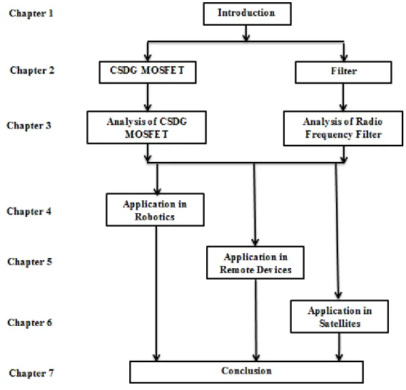
This research work aims to design a filter that can operate at high frequencies. Various circuits have been simulated using different components to achieve the desired results with improved performance. The organization of the thesis is as follows:
Figure 1.5. Research work structure.
Chapter 2 presents the literature review for this research work. The theories of the various types of filters and MOSFET’s have been discussed with their applications. The motivation for choosing a particular filter is detailed in this chapter as well. In addition
9
we look at the previous work that has been done by other researchers in the electronic filter field.
Chapter 3 focuses on the various designs that are used for both the Cylindrical Surrounding Double-Gate (CSDG) MOSFET and active High Pass Filter (HPF) in this research work.
Chapter 4 discusses the design of an active HPF that can be used in a robotic system. This filter makes use of both a transistor and an operational amplifier to provide the necessary gain. The designed filter is simulated with the aid of a software tool. These results are discussed and compared to an active high pass filter that makes use of two operational amplifiers. In addition a CSDG MOSFET has been implemented and added to the filter circuit to see what improvements it has on the overall gain of the circuit.
Chapter 5 focuses on the design of a CSDG MOSFET that can be used in an active high pass filter circuit to provide an improvement in gain. The CSDG MOSFET makes use of parallel capacitors that connect the gate and drain. By doing this the overall capacitance is reduced and will allow higher frequencies to be achieved. Results have been discussed for both circuits with and without the use of a CSDG MOSFET.
Chapter 6 details the design of a filter that can be used in a satellite communication system. This design also makes use of a CSDG MOSFET but an additional oxide layer is added to the MOSFET. Hafnium Silicate has been chosen to complement the existing Silicon layer. In addition we look at the effect that varying the forward current gain has on the gain of the filter.
Finally, we conclude this research work and recommend the future scope of the work in Chapter 7.
10
Chapter-2
Literature Review
In continuation from Chapter 1 (were RF filters has been discussed), we are using the CSDG MOSFET to design the novel filter. Therefore this chapter deals with the theory behind the CSDG MOSFET.
2.1
Bipolar Junction Transistor
The development of the Bipolar Junction Transistor (BJT) in 1948 guided the field of electronics in a new direction. This crystalline silicon structure as made it possible to design and manufacture devices that are both cost effective and have minimal weight. A BJ T is made up of 3 separate layers of doped semiconductor materials which can either be of PNP or NPN configuration and is illustrated in Figure 2.1. The difference in functionality between these two configurations is the biasing of the junctions when they are in operation. The NPN bipolar transistor contains a thin p-region between two n-regions. In contrast, the PNP bipolar transistor contains a thin n-region sandwiched between two p-regions [21].The three regions and their terminal connections are referred to as the emitter, base, and collector.
Figure 2.1. Simplified structure of bipolar transistors [21].
11
The BJT consists of a pair of PN junctions which are known has the emitter-base junction (EBJ) and the collector-base junction (CBJ). The different bias conditions of these junctions determine the various modes of operation. Some of these operations include active, cutoff, saturation and reverse-active modes [22]. Depending on the mode that the BJT operates at, it can either act as an amplifier or a switch.
2.2
MOSFET
Very Large Scale Integrated (VLSI) and Ultra Large Scale Integrated (ULSI) circuits make use of MOS technologies to make microprocessors, memory chips and analog integrated circuits (IC’s). Since the late 1970’s the MOSFET has been used extensively in electronic circuits for the following reasons:
Compared to a BJT it is smaller in size and requires a smaller area of silicon or similar material.
The process to manufacture these components is simple.
Digital logic and memory can be made with MOSFET’s only.
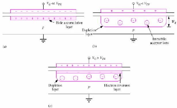
The heart of this structure is known as a MOS capacitor (Figure 2.3).This structure is composed of semiconductor substrate, an insulator film (SiO2 is commonly used), and
metal electrode (gate). The capacitance of the MOS structure depends on the voltage (bias) of the gate. Generally a voltage is applied to the gate (VG) whilst the body of the component is grounded.
12 Figure 2.4. Three modes of operation (a) accumulation, (b) depletion and (c) inversion of MOS capacitor
[24].
Figure 2.4 shows the three modes of operation of the MOS capacitor as accumulation, depletion and inversion modes respectively and is explained below:
(i) Accumulation - A positively applied gate voltage which is larger than the flat band voltage (VFB) brings about positive charge on the metal electrode (gate) and negative charge in the semiconductor.VFB is the voltage at which there is no charge in the MOS capacitor and hence there is no electric field across the oxide.
(ii) Depletion - If the applied VG is brought below the VFB, a negative charge is induced at the interface between the gate and the SiO2 oxide layer. This
results in a positive charge being induced at the oxide/semiconductor interface.
(iii) Inversion - If VG is lowered below the threshold voltage (VT); the semiconductor surface inverts its conduction type from n-type to p-type in our particular situation.
13
2.3
Double-Gate (DG) MOSFET
The DG MOSFET is an extension of the MOSFET concept and consists of two gates. The main idea of this improved type of MOSFET is to have a Si channel of very small width and to control the Si channel by applying gate contacts to both sides of the channel [25, 26]. The structure of the DG MOSFET consists of a conducting channel which is commonly undoped and is enclosed by gate electrodes at the top and bottom (Figure 2.5). These devices have an excellent gate control over the channel due to the sandwiching of Silicon on Insulator (SOI) between the two gates. The DG MOSFET makes use of volume inversion layer unlike the Single Gate (SG) MOSFET. Volume inversion carriers tend to experience less interference with the carriers than in the surface inversion layer due to more space and freedom of carrier and this leads to increase in the mobility of the DG MOSFET [27].
The DG MOSFET’s family consists of three types (i) Planar, (ii) Vertical and (iii) FinFET. Planar has both horizontal gates and channels whilst a Vertical DG MOSFET has conduction in the vertical direction. A FinFET has a vertical channel and its conduction is parallel to the water surface. From the three mentioned types the FinFET device has the simplest fabrication process and is thus the most popular type of DG MOSFFET. A DG MOSFET has a number of advantages over CMOS devices and some of these include [28-30]:
Nearly ideal subthreshold slope due to the voltage being applied on the gate terminals help to regulate the electric field which in turn determines the amount of supplied current through the channel.
Circuit speed is improved.
Small intrinsic gate capacitance and junction capacitances.
Short Channel Effects (SCE) is better suppressed since the gate to channel coupling is doubled.
Reduced Random Dopant Fluctuations (RDF) due to undoped or lightly doped body and reduced carrier mobility degradation.
Design flexibility at circuit level by symmetric/asymmetric with tied and independent gate options.
14 Figure 2.5. Double-Gate MOSFET structure [28].
The current driving capability of DG MOSFETs is twice that of planar CMOS and thus these devices can be operated at reduced input and threshold voltages. Hence power consumption is less in DG MOSFETs.
2.4
Gate All Around (GAA) MOSFET
The scaling of MOSFET transistors makes the use of innovative device geometries a necessity in order to solve the limitations of the technology that is currently available on the market [31]. Several concepts have been designed in the GAA family of MOSFETs with the two most common being of cylindrical or square shape. A cylindrical shaped GAA MOSFET can be simplified since the device can be analyzed in 1D whereas a square GAA MOSFET has to make use of more challenging techniques because we need to take into account that the cross-sections of these devices do not form a traditional squared shape. This imperfection happens during the manufacturing process when the substances experience a chemical imbalance which results in the edges having a rounded corner. Due to the technology that is currently available this effect is unavoidable but with the rapid growth of technology we will soon have squared GAA MOSFETs readily available. Aside from these two mentioned shapes, a promising design for a GAA based MOSFET makes use of nanowire technology [32]. It provides excellent electrostatic control over the channel which is bounded by a conducting gate and provides higher transconductance compared to the devices mentioned earlier in this chapter [33]. The insulation layer (SiO2) usually ranges from 1nm to 5nm.
15
2.5
Cylindrical Surrounding Gate MOSFET
MOSFET technology has already achieved perceptible level of performance by down scaling the dimensions [34]. However the problem arises when it comes to improving the devices electrostatic efficiency. A saturated device has dimensions which give rise to a number of issues such as high gate leakage current and various SCEs viz. threshold voltage roll-off, drain induced barrier lowering (DIBL) and increased substrate bias effect [35, 36]. However there have been numerous alterations to the general MOSFET devices structure in order to improve its performance and the geometry best suited to help minimize the above mentioned issues is in the form of a cylinder. This new device is known as the Cylindrical Surrounding Gate (CSG) MOSFET and provides exceptional gate controllability in comparison to single gate and other multi-gate structures. The CSG component in the fully depleted regime shows better robustness against SCEs and also reduces the threshold voltage and sub-threshold swing [37]. Figure 2.6 below shows a general CSG structure.
16
2.6
Cylindrical Surrounding Double-gate (CSDG) MOSFET
(This device is used and elaborated in this research work/thesis.)The CSDG MOSFET is extremely beneficial since it is composed of an undoped body which allows for the efficient controlling of the MOSFET channel by making use of a small channel width and due to its cylindrical structure, gate contact is applied to both the outer and inner sides of the MOSFET. This characteristic helps to reduce the SCE and will yield higher carrier mobility compared with the DG MOSFET or SG MOSFET and makes it an ideal choice for VLSI and nanotechnology designs. A CSDG MOSFET is an extension of the GAA device with scaling [38]. This type of MOSFET looked into how the use of circuit parameters such as capacitance, threshold voltage, frequency, switching speed and drain current can play a role in helping to improve shortcomings such as enhancing carrier mobility, current drive and reduce short channel effects [39].
The concept behind the operation of CSDG MOSFET is that it controls the Silicon channel width so that it has minimal contact with both sides of the channel. This idea helps to suppress the SCE and results in higher currents being achieved compared to a MOSFET that makes use of only a single gate. It is also observed that an n-doped layer in the channel reduces the threshold voltage and increases the drain current, when compared with a device of undoped channel. The reduction in the threshold voltage and the increase in the drain current occur with the level of doping [40, 41].
A larger leakage current is observed than that of an undoped channel but smaller than that of a uniformly doped channel. In particular, the CSDG MOSFET with an intrinsic channel is considered as the best option from the MOSFET family for device downscaling.
Figure 2.7 shows the basic model of combination of two MOSFETs attached to form an n-channel MOSFET. This structure is designed on a p-type semiconductor which serves as the Body (B) and comprises of two n-type semiconductors at the uppermost part of the Body and are known as the Source (S) and Drain (D). A metal electrode called the Gate (G1) can be seen above the p-type semiconductor and is kept apart from the semiconductor by a thin layer of SiO2 (Oxide 1). This thin layer acts as an electrical
insulator and occupies the space between the Source and Drain which makes the Gate electrically insulated from the Body [42, 43]. The bottom portion of Figure 2.7 also represents the MOSFET but in this case it shows an inverted view and this structure is a
17
DG MOSFET. To form a CSDG MOSFET, Figure 2.7 is then rotated along its reference point to form a cylindrical shape and can be seen in Figure 2.8. The CSDG MOSFET has two gates (G1 and G2, blue), a drain (red), Oxides (Oxide-1 and Oxide-2, yellow), and the p-type substrate (green).
18 Figure 2.8. Schematic of Cylindrical Surrounding Double Gate MOSFET. [38].
Gate-1 is formed in the inner portion of the cylinder, followed by the thin oxide which helps minimize the effect of SCE whilst the extended element of the cylinder is the Drain and Source. In the CSDG MOSFET, when suitable positive voltages are applied to the gates G1 and G2, the body which has the majority carrier as hole and minority carrier as electron will have the holes repelling from the insulators Oxide-1 and Oxide-2 and electrons attracted toward the insulator [41]. This establishes a channel for which electrons at the n substrate can move through the source to the drain. This channel is called the inversion layer [42, 44]. An increase in voltage potentials at both G1 and G2 will create a larger electric field which in turn creates a larger n-channel between the drain and the source. This is referred to as the enhancement mode of the MOSFET.
CSDG MOSFET’s have been used in a number of electronic circuits such as bridge rectifiers and boost regulators [45, 46]. In terms of a CSDG MOSFET being used in the RF and communications domain not much work has been done in this area. Oyedeji et. al. [47] recently proposed the design of an amplifier that made use of a CSDG MOSFET and can be seen in Figure 2.9. An amplifier is an electronic device that will increase a signal’s voltage, current or power. They are widely used in wireless communication, broadcasting and in audio equipment.
19 Figure 2.9. CSDG MOSFET based amplifier [47].
This work looked at addressing the operational transconconductance of an amplifier of small voltage in CSDG MOSFET. From the model that was created, it was found that the transconductance in a single CSDG MOSFET is more than that of a CSSG or any similar kind of DG MOSFET due to the structure of the device. This is another advantage of using a CSDG MOSEFT over another MOSFET structure. It was also found that the transconductance of the CSDG MOSFET is affected by the increase of the addition of both an inner and outer structure.
In conclusion, the CSDG MOSFET just like conventional MOSFET devices operates in three modes [48]:
Cut-off mode: The applied voltage (Vgs) is lesser than the threshold voltage (VT) and the device tends to be in the off state.
Linear mode: The applied voltage at the gate (Vgs) is greater than the threshold voltage and drain voltage (Vgs-VT>Vds) which leads to the formation of weak inversion channels between the oxide and the p-substrate.
Saturation mode: As the drain voltage increases, a saturation region will be reached (Vgs-VT<Vds). At this mode, the CSDG MOSFET is fully turned on, and the on-resistance reduces drastically. The CSDG MOSFET operates efficiently under this mode as a rectifier.
20
2.7
Filter
As explained in Chapter 1, filters perform the function of frequency selection by passing signals whose frequencies lie within a specified range whilst preventing the passing of those that fall outside this region. In addition to having low and high pass filters there are variations of these types of filters. Some of these include RC, RL, RLC, LC and LR filters. Each of the five mentioned filters consists of either a combination of a resistor, inductor or capacitor network and is driven by a voltage or a current source. These filters are known as passive filters. RC filters are commonly used for low and high pass filters whereas a RLC filter configuration is commonly used for band pass and band elimination filters.
Recently extensive research has been conducted to convert RC or RL circuits into an LC circuit [49]. This is done by LC circuit uniquely mapping the roots of either a RC or RL circuit so that it becomes easier to identify and extract the roots from the bode plot. In the analog circuit industry this accurate identification of roots can be used in applications ranging from amplifiers to filters [50, 51].
In addition to having passive filters we also have active filters. There have been a number of designs in the field of active filters and these filters make use of active components such as an operational amplifier and other electronic components like resistors and capacitors [52]. The advantage of using an active component is that it provides a filter circuit with amplification and gain control. Some of the other advantages include [53]:
A reduction in size of the filter circuit and thus reduces the overall weight of the circuit.
Performance and reliability of the filter are improved. These filters provide exceptional isolation between the separate stages since it has a high input impedance and a low output impedance.
Simpler design that that of a passive filter and can be used in a wider range of applications.
Cost of the circuit is minimized since operational amplifiers cost less and these circuits don’t make use of inductors.
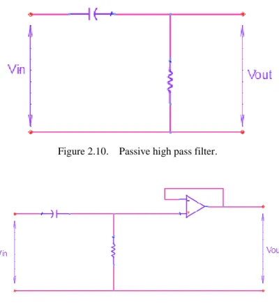
21 Figure 2.10. Passive high pass filter.
Figure 2.11. First order active high pass filter.
Figures 2.10 and 2.11 show a passive high pass filter and first order active high pass filter respectively.
2.8
Order of Filter
Filters are also designed for specific number of orders viz. first order, second order, third order, etc. [54]. The order of the filter refers to the number of components (either capacitors or inductors) that are part of the filter circuit. For an active circuit all the capacitors before the input of the active component are considered to have an effect on the order of the filter. For example, a first order RC high pass filter will consist of just a single capacitor and a second order filter will consist of two capacitors. A first and second order filter forms the basis for higher order filters (third, fourth, fifth, etc.).
An active high pass filter can be designed to meet a range of filter orders. Both first and second order filters are the building blocks for active filters that make use of orders that are greater than two. A general rule for the order for designing a filter, is an even order number will comprise of a number of cascaded second order filters only. An odd order filter will begin with a first order and then followed by a number of cascaded
22 Figure 2.12. Ideal frequency response of different filter orders.
second order filters [55]. From Figure 2.12, it can be seen that the higher the filter order, the closer the filter is to the ideal “brick wall” response.
The order of the filter is referred to as the maximum amount of delay the filter will have and it is directly proportional to the number of components needed to fulfill a particular filter’s specification. The advantages of using higher order filters include some of the following:
Narrower transition band.
More attenuation between the pass band and stop band.
Flatter pass band (less ripple).
There are a number of disadvantages to increasing the order of the filter and some of these include:
Longer group dely.
Cost to manufacture is greater has the order of filter is increased.
Higher chance of instability.
2.9
Components of Filter
The components that are used for a filter depends on what type of filter is being designed. There are three main types of filter circuits that are designed and these are (i) RC, (ii) RL and (iii) RLC circuits.The major difference between these two circuits is that
23
the former circuit stores energy in the form of the electric field whilst the latter circuit stores energy in the form of a magnetic field [53]. Electronic filters are continues-time filters that can be implemented with basic components such as resistors, capacitors, amplifiers or more complicated components such as active devices, which have been used for a long time in the field of engineering [56]. An RC circuit consists of a resistor and capacitor combination whereas a RL circuit makes use of a resistor and inductor combination. An RLC circuit consists of a resistor, an inductor and a capacitor connected either in series or parallel [52]. For this research work we look at the RC network configuration. The advantages of using this type of filter are the following:
(i) Mitigation of noise as this circuit does not create a magnetic field. (ii) Circuits are not bulky since it does not make use of an inductor.
(iii) Costs are kept to a minimum as capacitors use a more simple design compared to an inductor and they are more readily available.
24
Chapter-3
CSDG MOSFET and RF Filter Designs
This chapter looks at the detailed design of the CSDG MOSFET and 3rd order filters, which have been implemented in this research work. First we look at the design of the MOSFET’s that have been used for a robotics systems (Chapter 4), remote controlled devices (Chapter 5), and satellite communication systems (Chapter 6). Thereafter we document the equivalent filters that make use of the CSDG MOSFET. To further improve the gains and other parameters of the designed active high pass filters CSDG MOSFET’s are added to their outputs.
3.1
CSDG MOSFET Design
Three different configurations of CSDG MOSFET’s are designed and this is detailed in the subsections to follow. In sections 3.1.1, 3.1.2 and 3.1.3 we have designed MOSFET’s that can be used in robotic system, remote controlled devices, and satellite systems respectively.
From Equation 3.3 there are a number of parameters that can affect the overall capacitance of the CSDG MOSFET. The three parameters that were considered are length, circumference and permittivity of dielectric used. From Gaussian Law we can derive two equations (Equation 3.1 and Equation 3.2) that allows us to see what affect changing the three parameters over a desired range has on the electric field of a cylindrical device. E2 rL L o (3.1) 2 E r o (3.2)
The two equations above show us what type of relationship length, circumference and permittivity will have with the electric field. Circumference and permittivity both have an inversely proportional relationship with the electric field. This means that has the circumference or permittivity increases, the electric field will decrease and vice
25
versa. Length is directly proportional to electric field and thus if length is increased or decreased so will the electric field.
3.1.1. Basic Capacitive Model
Since capacitance plays such an important role in the selectivity of frequencies, by using a CSDG MOSFET to act as an additional capacitor. It will allow for better frequency selection and thus improvements in gain will be observed. The Single-Gate (SG) MOSFET for a number of years has been the choice of semiconductor device for Very Large Scale Integrated (VLSI) circuits. As explained in Chapter 2 of this research work, the CSDG MOSFET is an extension of a DG MOSFET with numerous benefits. It is at the forefront of MOSFET technology and research within this field is consistently growing [57]. It requires a small area of substrate due to its basic design and its fabrication costs are kept to a minimum [58]. However it does have its drawbacks such as mobility limitations, gate oxide used and leakage current. To reduce these limitations a new MOSFET structure has been proposed by Srivastava et al [46] and is known as a CSDG MOSFET. A CSDG MOSFET is formed by rotation of a DG MOSFET with respect to its reference point to form a hollow cylinder. This design is equivalent to two Single-Gate MOSFET brought together back-to-back and is then rotated 360° with respect to one of the gates [59].
The basic concept of CSDG MOSFET is to control the Si channel width so there is a smaller contact point at both sides of the channel, which is of cylindrical shape as shown in Figure 3.1. This concept aids in suppressing the SCE and leads to higher currents as compared with a MOSFET using a single gate. It consists of two gates, one drain and one source. For this proposed solution we look at a basic CSDG MOSFET design that makes use of a SiO2 layer and we analyse the results that are achieved after the newly
designed filter has been simulated. The following six equations are analysed for the design of a CSDG MOSFET [59]:
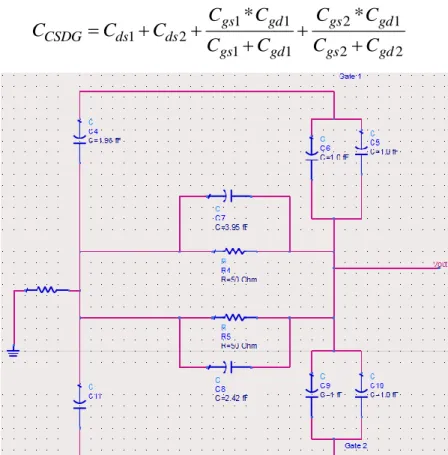
26 2 1 ln 2 1 ln 2 1 ln 2 2 ln 2 2 ln 2 2 ln t C gs a d a t C gd a d a L C ds a d a t C gs b b d t C gd b b d L C ds b b d
Where, ε is the Dielectric permittivity, a and b aretheinner and outer radius diameter respectively, L, t and d are length of cylinder, junction depth and depth of source respectively.
Figure 3.1. CSDG MOSFET [59].
27 Figure 3.2. Cross section of CSDG MOSFET [59].
For this design we have selected a = 5 nm, b = 12 nm, L = 20 nm, t = 10 nm, and d = 10 nm. The calculations for the required component values are calculated using the equations above: 2 1 1 ln t C C gs gd a d a (3.4) 12 9 2 *3.9 *8.85*10 *10 *10 9 9 5*10 10 *10 ln 9 5*10 0.003fF 2 2 2 ln t C C gs gd b b d (3.5) 12 9 2 *3.9 *8.85*10 *10 *10 9 12 *10 ln 9 9 12 *10 10 *10 0.002fF
28 2 1 ln L C ds a d a (3.6) 12 9 2 *3.9*8.85*10 * 20*10 9 9 5*10 10*10 ln 9 5*10 0.006fF 2 2 ln L C ds b b d (3.7) 12 9 2 *3.9*8.85*10 * 20*10 12*10 9 ln 9 9 12*10 10*10 0.006fF
29 3.1.2. Parallel Gate Capacitors
The capacitors that connect the gate and source are placed in parallel and are of equal capacitance as this will remove lower frequencies, because capacitance is inversely proportional to cutoff frequency as in Figure 3.4 [60].
For this design we have selected a = 5 nm, b = 12 nm, L = 20 nm, t = 10 nm, and d = 10 nm. For this design since parallel capacitors are used the following equations apply:
1 6 8 C C C gs (3.8) 2
6 6 8 C C C 2 9 10 C C C gs (3.9) 2
9 9 10 C C C The total capacitance across source to drain is given by the following expression:
1 1 2 1 1 2 1 1 2 2 * * gs gd gs gd CSDG ds ds gs gd gs gd C C C C C C C C C C C (3.10)
30 3.1.3. Hafnium Silicate Based CSDG MOSFET Model
The gate oxide that is most commonly used is SiO2 but due to the demand for circuits
to be more compact, the SiO2 layer produces high leakage current as the layer becomes
thinner (1.4 nm) [61]. To overcome leakage currents, high-k gate oxides (Table 1) are being used. Robertson [62] has proposed Hafnium Oxide (HfO2) or Hafnium Silicate
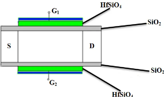
(HfSiO4) as an additional oxide layer. The CSDG MOSFET that is being designed
(Figure 3.8) makes use of HfSiO4 which has a lower dielectric constant and wider
band-gap compared to HfO2. The advantage of the former will allow the designed filter to
operate at higher frequencies and operate more efficiently since the need to store energy is linearly reduced.
In addition the overall capacitance of the MOSFET is reduced due to the lower dielectric constant and results in higher frequencies being achieved (frequency is inversely proportional to capacitance). Another advantage of using HfSiO4 is that, when
it is interfaced with the SiO2 layer, SCE is minimized. Since satellites operate at such
extreme temperatures, HfSiO4 can operate at temperatures above 2000°C and thus makes
it an ideal addition to the SiO2 layer.
A CSDG MOSFET makes use of two gates viz. an inner gate (G1) and an external gate (G2). The newly designed component has a layer of HfSiO4 between the gate and the Silicon layer (Figure 3.5 to Figure 3.7) to provide a better dielectric constant whilst providing an increase in performance. The gates on the silicon substrate will help to control the channel better compared to other CMOS devices.
Table 3.1 Table of High K Dielectric Materials
Dielectric Material Dielectric Constant (K) Gap (eV)
Silicon (Si) 1.1
Silicon Dioxide (SiO2) 3.9 9 Aluminium Oxide (Al2O3) 9 8.8
Titanium Oxide (TiO2) 80 3.5 Zirconium Dioxide (ZrO2) 25 5.8 Hafnium Oxide (HfO2) 25 5.8 Hafnium Silicate (HfSiO4) 11 6.5 Strontium Titanate (SrTiO3) 2000 3.2 Yttrium Oxide (Y2O3) 15 6 Lanthanum Oxide (La2O3) 30 6
31 Figure 3.5. Basic model of HfSiO4 based Double-Gate MOSFET.
Figure 3.6. Side view of CSDG MOSFET.
32 Figure 3.8. Capacitive model of CSDG MOSFET using HfSiO4.
Since satellite systems consist of a number of components, each component needs to be designed for a particular size whilst delivering the levels of performance that are required for the satellite to operate in an efficient manner. The designed CSDG MOSFET makes use of the following parameters to ensure that the filter remains compact: a = 3 nm, b = 6 nm, L = 10 nm and d = 5 nm.
Since this newly designed CSDG MOSFET makes use of two dielectric materials it results in the following effective dielectric material (Keff) and equivalent capacitance
33 2 4 2 4 * SiO HfSiO eff SiO HfSiO K K K K K (3.11) 2 4 2 4 * SiO HfSiO eq SiO HfSiO C C C C C
, where
C
SiO2 andC
HfSiO4are defined as:2 2 2 2 * SiO * SiO SiO K L C t
(3.12) 4 4 42 *
HfSiO*
HfSiO HfSiOK
L
C
t
(3.13)Figure 3.9. The oxide region of the MOSFET showing the materials used.
3.2
RF Filter Design
RF filters of all types are important elements in a number of applications ranging from audio to RF. This section will look at the design of a third order active high pass filter. Designing this type of filter is considered to be a difficult process but it can be simplified once the full specifications of the design are known. This allows decisions to be made on topology, filter type and components that can be used to meet the filter specifications.
Two significant parameters which illustrate the change in signal are known as gain (G) and phase shift (θ). Since both the gain and phase shift are parameters that depend on frequency they are said to be functions of frequency [63, 64]. They can thus be expressed by the following equations:
34 ( )
GG f (3.14) ( )f
(3.15) These two above functions represent the frequency response and the phase response of the designed active high pass filter respectively. In addition to these 2 parameters we also look at the return loss of the various third order filters that have been designed. To design this type of filter we simply cascade both first and second order active high pass filters. Below is the derivation for the cutoff frequency a first order filter [65, 66]:
Figure 3.10. First order filter.
1 * 1 V j in C c V out R j C c (3.16)
It is known that the cutoff frequency should be equated to a value of 1 2 . 1 1 1 2 j C c R j C c 1 1 2 2 1 2 C c R C c
35 2 1 2 1 2 * R C C c c 2 2 1 2 1 2* R R R c c 2 1 2 R C c 1 R C c Since, 2 f c c 1 2 f c RC
Figure 3.11. Second order filter.
The next derivation is of a second order filter and makes use of Kirchoff’s Current Law. The circuit shown in Figure 3.11 helps with this derivation.
0 2 2 V V out node sC V out R
1
2 2 V V sR C node out (3.17)36 0
1
1 2
V V V V
node in node out sC V
node R R
0 1 2 1 2 1 2 1 V R R sR R C R V R V node in out (3.18) Substitute equation 3.17 into equation 3.18 and rearranging we end up with following resulting equation:
1
2
2 2 1 2 1 2 1 1 V R out V sR C R R sR R C R in
1
2 1 1 2 1 2 1 1 1 2 2 2 s R R C C s R C R C R C Substituting s j the resulting equation is:
2
1 2 4 2 ( ) 2 1 1 2 1 2 1 1 1 2 2 2 1 2 1 2 R R C C R C R C R C R R C C It is known that the cutoff frequency should be equated to a value of 1 2 .
2
1 1 2 4 2 2 ( ) 2 1 1 2 1 2 1 1 1 2 2 2 1 2 1 2 R R C C R C R C R C R R C C
2 2
4 2 2 ( ) 2 1 1 2 1 2 1 1 1 2 2 2 1 2 1 2 R R C C R C R C R C R R C C
2 2 2 1 2 1 2 1 2 1 2 1 2 1 1 1 2 2 2 R R C C R R C C R C R C R C
2 1 1 2 1 2 R R C C 1 2 1 2 1 2 R R C C , hence 1 1 2 1 2 R R C C Since, 2 f c so 1 2 1 2 1 2 f c R R C C 37
After considering the advantages and disadvantages and doing extensive research, the order of filter that was chosen was a third order active high pass filter as this best allowed us to meet our specification targets. A factor is of paramount importance in the electronics industry is one of cost to manufacture and produce such equipment. After simulating other filters that made use of a fourth or fifth order, we observed that the differences in gain were not significant enough to warrant the extra cost and complexity of the design.
3.3
Analysis of Parameters
This section of the chapter looks analyzing the effect that length and radius will have on both the gain and cutoff frequency of a filter. When doing the analysis on length, other parameters such has radius, permittivity and depth of source were kept constant. Figures 3.12 and 3.13 show the gain and cutoff frequency respectively.
These results agreed with the theory learnt from Sections 3.1 and 3.2 of this chapter. From equation 3.3 we see that length is directly proportional to capacitance. Has the length of the cylinder is increased so does the capacitance. Since capacitance is inversely proportional to frequency, the frequency of the filter is decreased when capacitance is increased. This can be clearly seen in Figure 3.13. The difference in the frequency value may be a mere 0.25 but this small value can alter the bandwidth and the throughput of a device.
38 Figure 3.13. Length vs. Cutoff Frequency.
![Figure 1.4. -3 dB Curve of high pass filter [18].](https://thumb-us.123doks.com/thumbv2/123dok_us/9665131.2454482/22.892.141.775.121.610/figure-db-curve-high-pass-filter.webp)
![Figure 2.6. Cylindrical Surrounding Gate MOSFET structure [38].](https://thumb-us.123doks.com/thumbv2/123dok_us/9665131.2454482/32.892.297.626.590.1027/figure-cylindrical-surrounding-gate-mosfet-structure.webp)
![Figure 2.7. Basic model of combination of two MOSFETS back-to-back [38].](https://thumb-us.123doks.com/thumbv2/123dok_us/9665131.2454482/34.892.146.615.262.766/figure-basic-model-combination-mosfets.webp)
![Figure 3.1. CSDG MOSFET [59].](https://thumb-us.123doks.com/thumbv2/123dok_us/9665131.2454482/43.892.379.746.124.593/figure-csdg-mosfet.webp)