Description
The Atmel® | SMART SAM G55 is a series of Flash microcontrollers based on the high-performance 32-bit ARM® Cortex®-M4 RISC processor with FPU (Floating Point Unit). It operates at a maximum speed of 120 MHz and features 512 Kbytes of Flash and up to 176 Kbytes of SRAM. The peripheral set includes eight flexible communication units comprising USARTs, SPIs and I2C-bus interfaces (TWIs), two three-channel general-purpose 16-bit timers, two I2S controllers, one-channel pulse density modulation, one 8-channel 12-bit ADC, one real-time timer (RTT) and one real-time clock (RTC), both located in the ultra low-power backup area. The Atmel | SMART SAM G55 devices have three software-selectable low-power modes: Sleep, Wait and Backup. In Sleep mode, the processor is stopped while all other functions can be kept running. In Wait mode, all clocks and functions are stopped but some peripherals can be configured to wake up the system based on events, including partial asynchronous wakeup (SleepWalking™). In Backup mode, RTT, RTC and wakeup logic are running.
For power consumption optimization, the flexible clock system offers the capability of having different clock frequencies for some peripherals. Moreover, the processor and bus clock frequency can be modified without affecting the peripheral processing.
The real-time event management allows peripherals to receive, react to and send events in Active and Sleep modes without processor intervention.
TheSAM G55 devices are general-purpose low-power microcontrollers that offer high performance, processing power and small package options combined with a rich and flexible peripheral set. With this unique combination of features, the SAM G55 series is suitable for a wide range of applications including consumer, industrial control and PC peripherals.
The device operates from 1.62V to 3.6V and is available in three packages: 49-pin WLCSP, 64-pin QFN and 64-pin LQFP.
SAM G55G / SAM G55J
Atmel | SMART ARM-based Flash MCU
SUMMARY DATASHEET
Features
Core
̶ ARM Cortex-M4 with up to 16 Kbytes SRAM on I/D bus providing 0 wait state execution at up to 120 MHz (1)
̶ Memory Protection Unit (MPU)
̶ DSP Instructions
̶ Floating Point Unit (FPU)
̶ Thumb®-2 instruction set
Note: 1. 120 MHz with VDDCOREXT120 or with VDDCORE trimmed by regulator.
Memories
̶ Up to 512 Kbytes embedded Flash
̶ Up to 176 Kbytes embedded SRAM
̶ 8 Kbytes ROM with embedded boot loader, single-cycle access at full speed
System
̶ Embedded voltage regulator for single-supply operation
̶ Power-on reset (POR) and Watchdog for safe operation
̶ Quartz or ceramic resonator oscillators: 3 to 20 MHz with clock failure detection and 32.768 kHz for RTT or system clock
̶ High-precision 8/16/24 MHz factory-trimmed internal RC oscillator. In-application trimming access for frequency adjustment
̶ Slow clock internal RC oscillator as permanent low-power mode device clock
̶ PLL range from 48 MHz to 120 MHz for device clock
̶ PLL range from 24 MHz to 48 MHz for USB device and USB OHCI
̶ Up to 30 peripheral DMA (PDC) channels
̶ 256-bit General-Purpose Backup Registers (GPBR)
̶ 16 external interrupt lines
Peripherals
̶ 8 flexible communication units supporting:
USART
SPI
Two-wire Interface (TWI) featuring TWI masters and high-speed TWI slaves
̶ Crystal-less USB 2.0 Device and USB Host OHCI with On-chip Transceiver
̶ 2 Inter-IC Sound Controllers (I2S)
̶ 1 Pulse Density Modulation Interface (PDMIC) (supports up to two microphones)
̶ 2 three-channel 16-bit Timer/Counters (TC) with capture, waveform, compare and PWM modes
̶ 1 48-bit Real-Time Timer (RTT) with 16-bit prescaler and 32-bit counter
̶ 1 RTC with calendar and alarm features
̶ 1 32-bit Cyclic Redundancy Check Calculation Unit (CRCCU)
I/O
̶ Up to 48 I/O lines with external interrupt capability (edge or level), debouncing, glitch filtering and on-die series resistor termination. Individually programmable open-drain, pull-up and pull-down resistor and synchronous output
Analog
̶ One 8-channel ADC, resolution up to 12 bits, sampling rate up to 500 ksps
Package
̶ 49-lead WLCSP
̶ 64-lead LQFP
̶ 64-lead QFN
Operating Temperature Range
1.
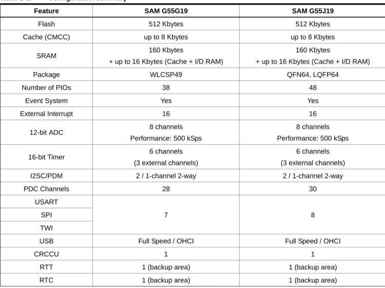
Configuration Summary
Table 1-1 summarizes the SAM G55 device configurations.
Table 1-1. Configuration Summary
Feature SAM G55G19 SAM G55J19
Flash 512 Kbytes 512 Kbytes
Cache (CMCC) up to 8 Kbytes up to 8 Kbytes
SRAM 160 Kbytes
+ up to 16 Kbytes (Cache + I/D RAM)
160 Kbytes
+ up to 16 Kbytes (Cache + I/D RAM)
Package WLCSP49 QFN64, LQFP64
Number of PIOs 38 48
Event System Yes Yes
External Interrupt 16 16
12-bit ADC 8 channels
Performance: 500 kSps
8 channels Performance: 500 kSps
16-bit Timer 6 channels
(3 external channels)
6 channels (3 external channels)
I2SC/PDM 2 / 1-channel 2-way 2 / 1-channel 2-way
PDC Channels 28 30
USART
7 8
SPI TWI
USB Full Speed / OHCI Full Speed / OHCI
CRCCU 1 1
RTT 1 (backup area) 1 (backup area)
2.
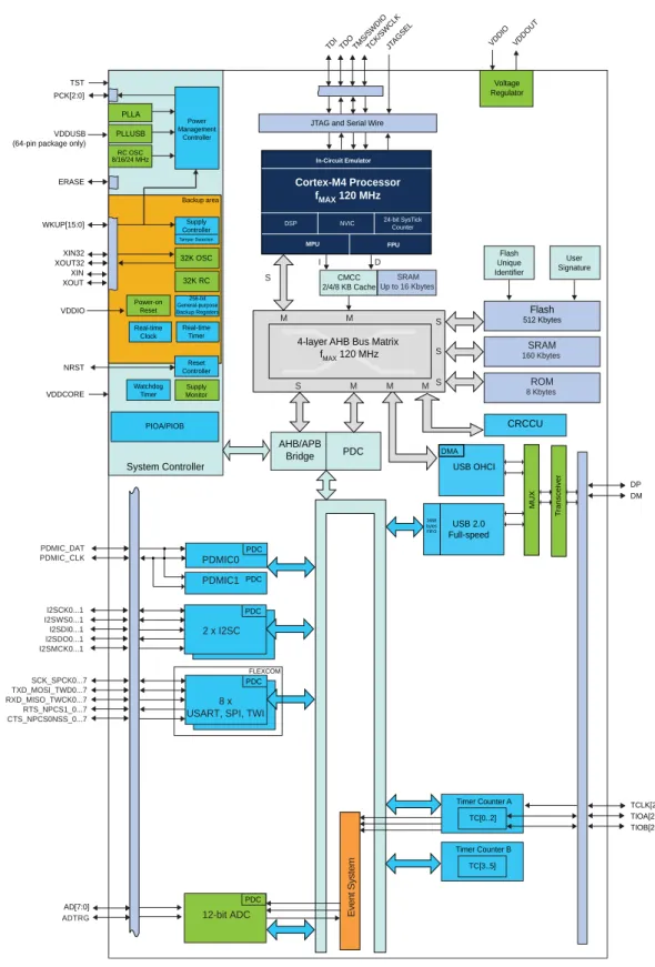
Block Diagram
Figure 2-1. SAM G55 Block Diagram
I D AHB/APB Bridge PCK[2:0] XIN32 XOUT32 ERASE VDDCORE ADTRG System Controller TCK/SWCLK
TDI TDO JTAGSEL VDDIO VDDOUT
JTAG and Serial Wire
Flash Unique Identifier Voltage Regulator TST 12-bit ADC TCLK[2:0] TIOA[2:0] TIOB[2:0] USB 2.0 Full-speed In-Circuit Emulator MPU Cortex-M4 Processor fMAX 120 MHz
NVIC 24-bit SysTick Counter DSP Flash 512 Kbytes DP DM PDC User Signature WKUP[15:0] FPU MUX T ransceiver VDDIO XIN XOUT VDDUSB (64-pin package only)
NRST AD[7:0] PIOA/PIOB TMS/SWDIO PDC Timer Counter A TC[0..2] Timer Counter B TC[3..5] SRAM 160 Kbytes ROM 8 Kbytes Event System S SRAM Up to 16 Kbytes Watchdog Timer PLLA Power Management Controller RC OSC 8/16/24 MHz PLLUSB CMCC 2/4/8 KB Cache CRCCU 8 x USART, SPI, TWI
PDC 2668 bytes FIFO Supply Monitor USB OHCI I2SDI0...1 I2SWS0...1 I2SCK0...1 I2SDO0...1 I2SMCK0...1 2 x I2SC PDC PDMIC_CLK PDMIC_DAT PDMIC0 PDC PDMIC1 PDC DMA Backup area Power-on Reset 32K OSC 32K RC Supply Controller Real-time Timer Real-time Clock Tamper Detection RXD_MISO_TWCK0...7 TXD_MOSI_TWD0...7 SCK_SPCK0...7 RTS_NPCS1_0...7 CTS_NPCS0NSS_0...7 FLEXCOM Reset Controller 256-bit General-purpose Backup Registers
4-layer AHB Bus Matrix fMAX 120 MHz S S S S M M M M M
3.
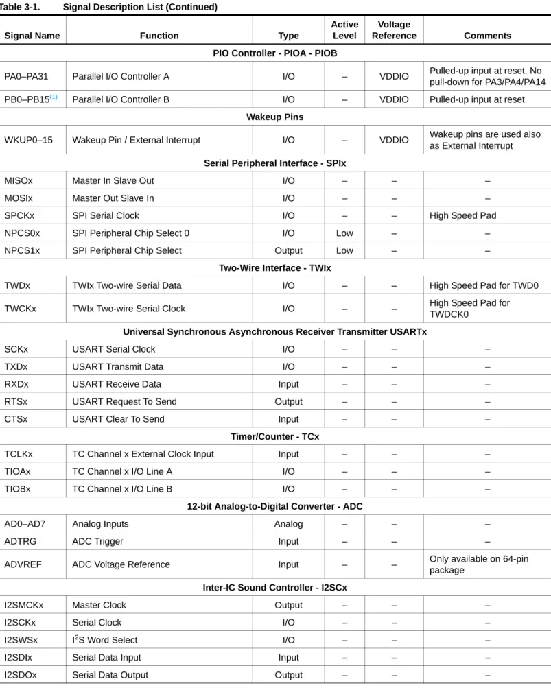
Signal Description
Table 3-1 gives details on the signal names classified by peripheral.
Table 3-1. Signal Description List
Signal Name Function Type
Active Level
Voltage
Reference Comments
Power Supplies
VDDIO Peripheral I/O Lines, Voltage Regulator,
ADC Power Supply Power – – 1.62V to 3.6V
VDDOUT Voltage Regulator Output Power – – 1.08V to 1.32V
VDDCORE Core Chip Power Supply Power – –
Connected externally to VDDOUT or VDDCOREXT100 or VDDCOREXT120
VDDUSB USB Power Supply Power – – Only available on 64-pin
package
GND Ground Ground – – –
Clocks, Oscillators and PLLs
XIN Main Oscillator Input Input – VDDIO Reset state:
- PIO input
- Internal pull-up disabled - Schmitt Trigger enabled
XOUT Main Oscillator Output Output – –
XIN32 Slow Clock Oscillator Input Input – VDDIO
XOUT32 Slow Clock Oscillator Output Output – –
PCK0–PCK2 Programmable Clock Output Output – –
Reset state: - PIO input
- Internal pull-up enabled - Schmitt Trigger enabled ICE and JTAG
TCK Test Clock Input – VDDIO No pull-up resistor
TDI Test Data In Input – VDDIO No pull-up resistor
TDO Test Data Out Output – VDDIO –
TRACESWO Trace Asynchronous Data Out Output – VDDIO –
SWDIO Serial Wire Input/Output I/O – VDDIO –
SWCLK Serial Wire Clock Input – VDDIO –
TMS Test Mode Select Input – VDDIO No pull-up resistor
JTAGSEL JTAG Selection Input High VDDIO Pull-down resistor
Flash Memory
ERASE Flash and NVM Configuration Bits Erase
Command Input High VDDIO Pull-down (15 kΩ) resistor
Reset/Test
NRST Microcontroller Reset I/O Low VDDIO Pull-up resistor
PIO Controller - PIOA - PIOB
PA0–PA31 Parallel I/O Controller A I/O – VDDIO Pulled-up input at reset. No
pull-down for PA3/PA4/PA14
PB0–PB15(1) Parallel I/O Controller B I/O – VDDIO Pulled-up input at reset
Wakeup Pins
WKUP0–15 Wakeup Pin / External Interrupt I/O – VDDIO Wakeup pins are used also
as External Interrupt Serial Peripheral Interface - SPIx
MISOx Master In Slave Out I/O – – –
MOSIx Master Out Slave In I/O – – –
SPCKx SPI Serial Clock I/O – – High Speed Pad
NPCS0x SPI Peripheral Chip Select 0 I/O Low – –
NPCS1x SPI Peripheral Chip Select Output Low – –
Two-Wire Interface - TWIx
TWDx TWIx Two-wire Serial Data I/O – – High Speed Pad for TWD0
TWCKx TWIx Two-wire Serial Clock I/O – – High Speed Pad for
TWDCK0 Universal Synchronous Asynchronous Receiver Transmitter USARTx
SCKx USART Serial Clock I/O – – –
TXDx USART Transmit Data I/O – – –
RXDx USART Receive Data Input – – –
RTSx USART Request To Send Output – – –
CTSx USART Clear To Send Input – – –
Timer/Counter - TCx
TCLKx TC Channel x External Clock Input Input – – –
TIOAx TC Channel x I/O Line A I/O – – –
TIOBx TC Channel x I/O Line B I/O – – –
12-bit Analog-to-Digital Converter - ADC
AD0–AD7 Analog Inputs Analog – – –
ADTRG ADC Trigger Input – – –
ADVREF ADC Voltage Reference Input – – Only available on 64-pin
package Inter-IC Sound Controller - I2SCx
I2SMCKx Master Clock Output – – –
I2SCKx Serial Clock I/O – – –
I2SWSx I2S Word Select I/O – – –
I2SDIx Serial Data Input Input – – –
I2SDOx Serial Data Output Output – – –
Table 3-1. Signal Description List (Continued)
Signal Name Function Type
Active Level
Voltage
Note: 1. Pull-up disabled on PB8/PB9.
Pulse Density Modulation Interface Controller - PDMICx
PDMIC_CLK Pulse Density Modulation Clock Output – – –
PDMIC_DAT Pulse Density Modulation Data Input – – –
USB OHCI/FS - USB
DM USB Data -Analog, Digital – WLCSP49: VDDIO 64-pin package: VDDUSB DM and DP in PIO configuration DP USB Data +
Table 3-1. Signal Description List (Continued)
Signal Name Function Type
Active Level
Voltage
4.
Package and Pinout
4.1
49-ball WLCSP Pinout
Table 4-1. SAM G55 Packages
Device Package
SAM G55G19 WLCSP49
SAM G55J19
QFN64 LQFP64
Table 4-2. SAM G55G19 49-ball WLCSP Pinout
A1 PA9 B6 NRST D4 PB10 F2 PA19/AD2
A2 GND B7 PB12 D5 PA1 F3 PA17/AD0
A3 PA24 C1 VDDCORE D6 PA5 F4 PA21
A4 PB8/XOUT C2 PA11 D7 VDDCORE F5 PA23
A5 PB9/XIN C3 PA12 E1 PB2/AD6 F6 PA16
A6 PB4 C4 PB6 E2 PB0/AD4 F7 PA8/XOUT32
A7 VDDIO C5 PA4 E3 PA18/AD1 G1 VDDIO
B1 PB11 C6 PA3 E4 PA14 G2 VDDOUT
B2 PB5 C7 PA0 E5 PA10 G3 GND
B3 PB7 D1 PA13 E6 TST G4 VDDIO
B4 PA2 D2 PB3/AD7 E7 PA7/XIN32 G5 PA22
B5 JTAGSEL D3 PB1/AD5 F1 PA20/AD3 G6 PA15
4.2
64-lead QFN/LQFP Pinout
4.2.1 64-lead QFN / LQFP Pinout
Note: 1. The bottom pad of the QFN package must be tied to ground.
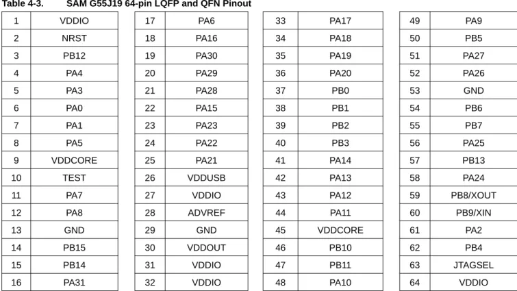
Table 4-3. SAM G55J19 64-pin LQFP and QFN Pinout
1 VDDIO 17 PA6 33 PA17 49 PA9
2 NRST 18 PA16 34 PA18 50 PB5
3 PB12 19 PA30 35 PA19 51 PA27
4 PA4 20 PA29 36 PA20 52 PA26
5 PA3 21 PA28 37 PB0 53 GND
6 PA0 22 PA15 38 PB1 54 PB6
7 PA1 23 PA23 39 PB2 55 PB7
8 PA5 24 PA22 40 PB3 56 PA25
9 VDDCORE 25 PA21 41 PA14 57 PB13
10 TEST 26 VDDUSB 42 PA13 58 PA24
11 PA7 27 VDDIO 43 PA12 59 PB8/XOUT
12 PA8 28 ADVREF 44 PA11 60 PB9/XIN
13 GND 29 GND 45 VDDCORE 61 PA2
14 PB15 30 VDDOUT 46 PB10 62 PB4
15 PB14 31 VDDIO 47 PB11 63 JTAGSEL
5.
Mechanical Characteristics
5.1
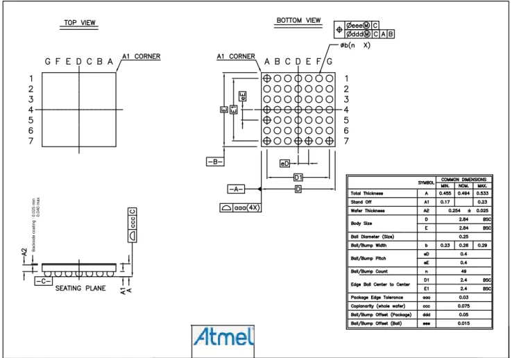
49-lead WLCSP Package
Figure 5-1. 49-lead WLCSP Package Mechanical Drawing
Backside coating : 0.025 min
5.2
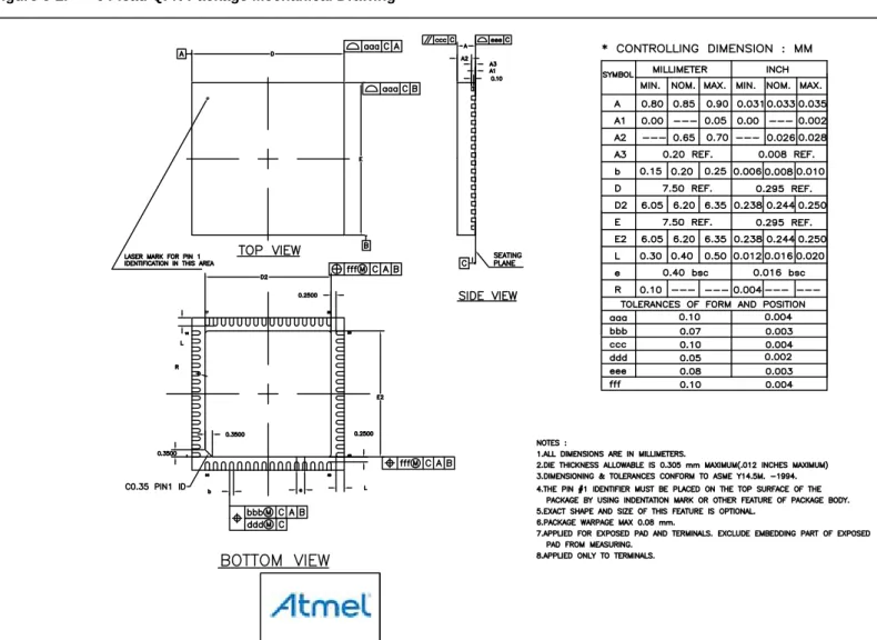
64-lead QFN Package
5.3
64-lead LQFP Package
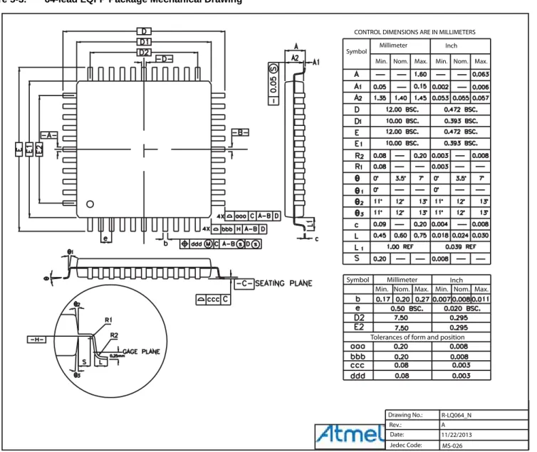
Figure 5-3. 64-lead LQFP Package Mechanical Drawing
CONTROL DIMENSIONS ARE IN MILLIMETERS
Millimeter Inch Symbol
Min. Nom. Max. Min. Nom. Max.
Symbol Millimeter Inch Min. Nom. Max. Min. Nom. Max.
Tolerances of form and position
Drawing No.: R-LQ064_N Rev.: A Date: 11/22/2013 Jedec Code: MS-026
6.
Ordering Information
Table 6-1. SAM G55 Ordering Information
Ordering Code MRL Package Carrier Type
Operating Temperature Range ATSAMG55G19A-UUT A WLCSP49 Reel Industrial -40°C to 85°C ATSAMG55G19B-UUT B ATSAMG55J19A-MU A QFN64 Tray Industrial -40°C to 85°C ATSAMG55J19B-MU B ATSAMG55J19A-MUT A Reel ATSAMG55J19B-MUT B ATSAMG55J19A-AU A LQFP64 Tray Industrial -40°C to 85°C ATSAMG55J19B-AU B ATSAMG55J19A-AUT A Reel ATSAMG55J19B-AUT B
7.
Revision History
In the tables that follow, the most recent version of the document appears first.
Table 7-1. SAM G55 Summary Datasheet Rev. 11289ES Revision History
Issue Date Changes
25-May-16
“Features”: “USB 2.0 Device” changed to “Crystal-less USB 2.0 Device” Table 1-1 “Configuration Summary”: removed instance of “TWIHS”
Figure 2-1 “SAM G55 Block Diagram”: repositioned ‘VUSB’ input and renamed to ‘VDDUSB’
Table 3-1 “Signal Description List”: renamed ‘VUSB’ to ‘VDDUSB’; inserted row “Pulse Density Modulation Interface Controller - PDMICx”; “USB OHCI/FS/IC” changed to “USB OHCI/FS”
Table 6-1 “SAM G55 Ordering Information”: added MRL B ordering codes
Table 7-2. SAM G55 Summary Datasheet Rev. 11289DS Revision History
Issue Date Changes
01-Dec-15
Updated “Description”
Modified “Features” (Note in “Core” section & “Up to 48 I/O lines” instead of “Up to 32 I/O lines” in “I/O “section) Updated Figure 2-1 “SAM G55 Block Diagram”
Table 3-1 “Signal Description List”:
- modified comments on VDDCORE, DM and DP
- PDMCLK0 changed to PDMIC_CLK; PDMDAT0 changed to PDMIC_DAT
Table 7-3. SAM G55 Summary Datasheet Rev. 11289CS Revision History
Issue Date Changes
16-Jun-15
Removed “Preliminary Status” marking. Modified Section ”Description”
Updated Figure 2-1 “SAM G55 Block Diagram”(GPBR) Added note to PB0/PB15 in Table 3-1 “Signal Description List” Added note to Section 4.2.1 “64-lead QFN / LQFP Pinout”
Replaced ATSAMG55J19-A-AUT with ATSAMG55J19A-AUT in Table 6-1 “SAM G55 Ordering Information”
Table 7-4. SAM G55 Summary Datasheet Rev. 11289BS Revision History
Issue Date Changes
14-Jan-15 Added “Preliminary Status” marking.
Table 7-5. SAM G55 Summary Datasheet Rev. 11289AS Revision History
Issue Date Changes
X
X X
X
X
X
ARM Connected Logo
Atmel Corporation 1600 Technology Drive, San Jose, CA 95110 USA T: (+1)(408) 441.0311 F: (+1)(408) 436.4200 | www.atmel.com © 2016 Atmel Corporation. / Rev.: Atmel-11289ES-ATARM-SAM-G55G-SAM-G55J-Summary Datasheet_25-May-16.
Atmel®, Atmel logo and combinations thereof, Enabling Unlimited Possibilities®, and others are registered trademarks or trademarks of Atmel Corporation in U.S. and other countries. ARM®, ARM Connected® logo, and others are the registered trademarks or trademarks of ARM Ltd. Other terms and product names may be trademarks of others.
DISCLAIMER: The information in this document is provided in connection with Atmel products. No license, express or implied, by estoppel or otherwise, to any intellectual property right is granted by this document or in connection with the sale of Atmel products. EXCEPT AS SET FORTH IN THE ATMEL TERMS AND CONDITIONS OF SALES LOCATED ON THE ATMEL WEBSITE, ATMEL ASSUMES NO LIABILITY WHATSOEVER AND DISCLAIMS ANY EXPRESS, IMPLIED OR STATUTORY WARRANTY RELATING TO ITS PRODUCTS INCLUDING, BUT NOT LIMITED TO, THE IMPLIED WARRANTY OF MERCHANTABILITY, FITNESS FOR A PARTICULAR PURPOSE, OR NON-INFRINGEMENT. IN NO EVENT SHALL ATMEL BE LIABLE FOR ANY DIRECT, INDIRECT, CONSEQUENTIAL, PUNITIVE, SPECIAL OR INCIDENTAL DAMAGES (INCLUDING, WITHOUT LIMITATION, DAMAGES FOR LOSS AND PROFITS, BUSINESS INTERRUPTION, OR LOSS OF INFORMATION) ARISING OUT OF THE USE OR INABILITY TO USE THIS DOCUMENT, EVEN IF ATMEL HAS BEEN ADVISED OF THE POSSIBILITY OF SUCH DAMAGES. Atmel makes no representations or warranties with respect to the accuracy or completeness of the contents of this document and reserves the right to make changes to specifications and products descriptions at any time without notice. Atmel does not make any commitment to update the information contained herein. Unless specifically provided otherwise, Atmel products are not suitable for, and shall not be used in, automotive applications. Atmel products are not intended, authorized, or warranted for use as components in applications intended to support or sustain life.
SAFETY-CRITICAL, MILITARY, AND AUTOMOTIVE APPLICATIONS DISCLAIMER: Atmel products are not designed for and will not be used in connection with any applications where the failure of such products would reasonably be expected to result in significant personal injury or death (“Safety-Critical Applications”) without an Atmel officer's specific written