Future Technology
Devices International Ltd
.FT221X
(USB 8-Bit SPI/FT1248 IC)
The FT221X is a USB to FTDI‟s
proprietary FT1248 interface with the
following advanced features:
Single chip USB to 1, 2, 4, or 8 bit wide synchronous interface.
Similar to an SPI Slave with variable bus width.
Entire USB protocol handled on the chip. No USB specific firmware programming required. Fully integrated 2048 byte multi-time-programmable (MTP) memory, storing device descriptors and CBUS I/O configuration. Fully integrated clock generation with no
external crystal required plus optional clock output selection enabling a glue-less interface to external MCU or FPGA.
Data transfer rates to 1MByte/s.
512 byte receive buffer and 512 byte transmit buffer utilising buffer smoothing technology to allow for high data throughput. FTDI‟s royalty-free Virtual Com Port (VCP)
and Direct (D2XX) drivers eliminate the requirement for USB driver development in most cases.
Configurable CBUS I/O pin.
USB Battery Charger Detection. Allows for USB peripheral devices to detect the presence of a higher power source to enable improved charging.
Device supplied pre-programmed with unique USB serial number.
USB Power Configurations; supports bus- powered, self-powered and bus-powered with power switching.
Integrated +3.3V level converter for USB I/O. True 3.3V CMOS drive output and TTL input;
operates down to 1V8 with external pull-ups. Configurable I/O pin output drive strength; 4
mA(min) and 16 mA(max)
Integrated power-on-reset circuit.
Fully integrated AVCC supply filtering - no external filtering required.
+ 5V Single Supply Operation. Internal 3V3/1V8 LDO regulators
Low operating and USB suspend current; 8mA (active-typ) and 125uA (suspend-typ).
Low USB bandwidth consumption.
UHCI/OHCI/EHCI host controller compatible. USB 2.0 Full Speed capable.
Extended operating temperature range; -40 to 85⁰C.
Available in compact Pb-free 20 Pin SSOP and QFN packages (both RoHS compliant).
Neither the whole nor any part of the information contained in, or the product described in this manual, may be adapted or reproduced in any material or electronic form without the prior written consent of the copyright holder. This product and its documentation are supplied on an as-is basis and no warranty as to their suitability for any particular purpose is either made or implied. Future Technology Devices International Ltd will not accept any claim for damages howsoever arising as a result of use or failure of this product. Your statutory rights are not affected. This product or any variant of it is not intended for use in any medical appliance, device or system in which the failure of the product might reasonably be expected to result in personal injury. This document provides preliminary information that may be subject to change without notice. No freedom to use patents or other intellectual property rights is implied by the publication of this document. Future Technology Devices International Ltd, Unit 1, 2 Seaward Place, Centurion Business Park, Glasgow G41 1HH United Kingdom. Scotland Registered Company Number: SC136640
1
Typical Applications
USB to SPI slave interface in 1-bit mode Upgrading Legacy Peripherals to USB Utilising USB to add system modularity Incorporate USB interface to enable PC
transfers for development system communication
Interfacing MCU/PLD/FPGA based designs to add USB connectivity
USB Industrial Control USB MP3 Player Interface
USB FLASH Card Reader and Writers Set Top Box PC - USB interface USB Digital Camera Interface
Dedicated Charging Port detection for enabling higher current battery charging.
1.1
Driver Support
Royalty free VIRTUAL COM PORT (VCP) DRIVERS for...
Windows 7 32,64-bit
Windows Vista and Vista 64-bit Windows XP and XP 64-bit Server 2003, XP and Server 2008 Windows XP Embedded
Windows CE 4.2, 5.0 and 6.0 Mac OS-X
Linux 3.2 and greater Android
Royalty free D2XX Direct Drivers (USB Drivers + DLL S/W Interface)
Windows 7 32,64-bit
Windows Vista and Vista 64-bit Windows XP and XP 64-bit Server 2003, XP and Server 2008 Windows XP Embedded
Windows CE 4.2, 5.0 and 6.0 Mac OS-X
Linux 2.6 and greater Android
The drivers listed above are all available to download for free from FTDI website (www.ftdichip.com). Various 3rd party drivers are also available for other operating systems - see FTDI website
(www.ftdichip.com) for details.
For driver installation, please refer to http://www.ftdichip.com/Documents/InstallGuides.htm
1.2
Part Numbers
Part Number Package
FT221XQ-x 20 Pin QFN
FT221XS-x 20 Pin SSOP
Note: Packing codes for x is:
- R: Taped and Reel, (SSOP is 3,000pcs per reel, QFN is 5,000pcs per reel). - U: Tube packing, 58pcs per tube (SSOP only)
1.3
USB Compliant
The FT221X is fully compliant with the USB 2.0 specification and has been given the USB-IF Test-ID (TID) 40001334 (Rev B).
2
FT221X Block Diagram
3.3 Volt LDO Regulator 1.8 Volt LDO Regulator USB Transceiver with Integrated 1.5k pullups and battery charge detection USB DPLL Internal 12MHz Oscillator X4 Clock Multiplier Serial Interface Engine (SIE) USB Protocol Engine FT1248 Controller Reset Generator FIFO TX Buffer (512 bytes) FIFO RX Buffer (512 bytes) Internal MTP Memory 48MHz GND RESET# To USB Transceiver Cell3V3OUT VCCIO 3V3OUT VCC USBDP USBDM 1V8 Internal Core Supply MIOSI[0] MIOSI[1] MIOSI[2] MIOSI[3] MIOSI[4] MIOSI[5] MIOSI[6] MISOI[7] CLK CS# MISO CBUS3
Figure 2.1 FT221X Block Diagram
Table of Contents
1
Typical Applications ... 2
1.1
Driver Support ... 2
1.2
Part Numbers... 2
1.3
USB Compliant ... 3
2
FT221X Block Diagram ... 4
3
Device Pin Out and Signal Description ... 7
3.1
20-LD QFN Package ... 7
3.1.1 QFN Package Pin Out Description ... 7
3.2
20-LD SSOP Package... 9
3.2.1 SSOP Package Pin Out Description ... 9
3.3
CBUS Signal Options ... 11
4
Function Description... 13
4.1
Key Features ... 13
4.2
Functional Block Descriptions ... 13
5
FT1248 Interface Description. ... 15
5.1
Determining the Dynamic Bus Width ... 15
5.2
Supported Commands on the FT1248 Interface ... 16
5.3
LSB or MSB Selection ... 17
5.4
Clock Phase/Polarity ... 17
5.4.1 CPHA = 1 ... 18
5.5
FT1248 Timing ... 19
6
Devices Characteristics and Ratings ... 21
6.1
Absolute Maximum Ratings... 21
6.2
ESD and Latch-up Specifications ... 21
6.3
DC Characteristics... 22
6.4
MTP Memory Reliability Characteristics ... 26
6.5
Internal Clock Characteristics ... 26
7
USB Power Configurations ... 27
7.1
USB Bus Powered Configuration ... 27
7.2
Self Powered Configuration ... 27
7.3
USB Bus Powered with Power Switching Configuration ... 29
7.4
USB Battery Charging Detection ... 30
8
Application Examples ... 32
8.1
USB to FT1248 Converter ... 32
9
Internal MTP Memory Configuration ... 36
9.1
Default Values ... 36
9.2
Methods of Programming the MTP Memory ... 37
9.2.1 Programming the MTP memory over USB ... 37
9.2.2 Programming the MTP memory over FT1248 ... 37
9.3
Memory Map ... 38
9.4
Hardware Requirements ... 39
9.5
Protocol ... 39
9.5.1 Address MTP memory (0x05) ... 39 9.5.2 Write MTP memory (0x06) ... 39 9.5.3 Read MTP memory (0x07) ... 399.5.4 Examples of Writing and Reading ... 39
10
Package Parameters ... 41
10.1
SSOP-20 Package Mechanical Dimensions ... 41
10.2
SSOP-20 Package Markings ... 42
10.3
QFN-20 Package Mechanical Dimensions ... 43
10.4
QFN-20 Package Markings ... 44
10.5
Solder Reflow Profile ... 45
11
Contact Information ... 46
Appendix A – References ... 47
Appendix B - List of Figures and Tables ... 48
3
Device Pin Out and Signal Description
3.1
20-LD QFN Package
V
C
C
IO
2
0
MIOSI7
2
MIOSI4
18
G
N
D
3
MIOSI5
4
MIOSI2
19
MIOSI3
6
MISO
7
USBDP
8
USBDM
9
3V3OUT
10
RESET#
11
V
C
C
1
2
CS#
14
CLK
15
G
N
D
1
3
MIOSI0
17
MIOSI6
5
MIOSI1
1
CBUS3
16
G
N
D
2
1
Figure 3.1 QFN Schematic Symbol
3.1.1
QFN Package PinOut Description
Note : # denotes an active low signal.
Pin No. Name Type Description
12 **
VCC
POWER
Input 5 V (or 3V3) supply to IC
20 VCCIO POWER
Input 1V8 - 3V3 supply for the IO cells
10 **
3V3OUT
POWER Output
3V3 output at 50mA. May be used to power VCCIO. When VCC is 3V3; pin 10 is an input pin and should be connected to pin 12
3, 13 GND POWER
Input 0V Ground input.
Table 3.1 Power and Ground
*Pin 21 is the centre pad under the IC. Connect to GND.
Pin No. Name Type Description
9 USBDM INPUT USB Data Signal Minus. 8 USBDP INPUT USB Data Signal Plus. 11 RESET# INPUT Reset input (active low).
Table 3.2 Common Function pins
Pin No. Name Type Description
17 MIOSI[0] I/O Bi-Directional data bit 0 1 MIOSI[1] I/O Bi-Directional data bit 1 19 MIOSI[2] I/O Bi-Directional data bit 2 6 MIOSI[3] I/O Bi-Directional data bit 3 18 MIOSI[4] I/O Bi-Directional data bit 4 4 MIOSI[5] I/O Bi-Directional data bit 5 5 MIOSI[6] I/O Bi-Directional data bit 6
2 MIOSI[7] I/O Bi-Directional data bit 7
15 CLK Input Clock input from FT1248 interface master
14 CS# Input Chip select input to enable the device interface. Active low logic.
7 MISO Output Master In Serial Out. Used to provide status information to the FT1248 interface master.
16 CBUS3 I/O Configurable CBUS I/O Pin. Function of this pin is configured in the device MTP memory. See CBUS Signal Options, Table 3.7.
Table 3.3 FT1248 Interface and CBUS Group (see note 1)
Notes:
1. When used in Input Mode, the input pins are pulled to VCCIO via internal 75kΩ (approx) resistors. These pins can be programmed to gently pull low during USB suspend (PWREN# = “1”) by setting an option in the MTP memory.
3.2
20-LD SSOP Package
MIOSI1
4
MIOSI7
5
G
N
D
6
MIOSI5
7
MIOSI6
8
MIOSI3
9
MISO
10
USBDP
11
USBDM
12
3V3OUT
13
RESET#
14
V
C
C
1
5
G
N
D
1
6
CS#
17
CLK
18
CBUS3
19
MIOSI0
20
MIOSI4
1
MIOSI2
2
V
C
C
IO
3
Figure 3.2 SSOP Schematic Symbol
3.2.1
SSOP Package PinOut Description
Note : # denotes an active low signal.Pin No. Name Type Description
15 **
VCC
POWER
Input 5 V (or 3V3) supply to IC
3 VCCIO POWER
Input 1V8 - 3V3 supply for the IO cells
13 **
3V3OUT
POWER Output
3V3 output at 50mA. May be used to power VCCIO. When VCC is 3V3; pin 13 is an input pin and should be connected to pin 15.
6, 16 GND POWER
Input 0V Ground input.
Table 3.4 Power and Ground
** If VCC is 3V3 then 3V3OUT must also be driven with 3V3 input
Pin No. Name Type Description
12 USBDM INPUT USB Data Signal Minus. 11 USBDP INPUT USB Data Signal Plus. 14 RESET# INPUT Reset input (active low).
Pin No. Name Type Description
20 MIOSI[0] I/O Bi-Directional data bit 0 4 MIOSI[1] I/O Bi-Directional data bit 1 2 MIOSI[2] I/O Bi-Directional data bit 2 9 MIOSI[3] I/O Bi-Directional data bit 3 1 MIOSI[4] I/O Bi-Directional data bit 4 7 MIOSI[5] I/O Bi-Directional data bit 5 8 MIOSI[6] I/O Bi-Directional data bit 6
5 MIOSI[7] I/O Bi-Directional data bit 7
18 CLK Input Clock input from FT1248 interface master
17 CS# Input Chip select input to enable the device interface. Active low logic.
10 MISO Output Master In Serial Out. Used to provide status information to the FT1248 interface master.
19 CBUS3 I/O Configurable CBUS I/O Pin. Function of this pin is configured in the device MTP memory. See CBUS Signal Options, Table 3.7.
Table 3.6 FT1248 Interface and CBUS Group (see note 1)
Notes:
1. When used in Input Mode, the input pins are pulled to VCCIO via internal 75kΩ (approx) resistors. These pins can be programmed to gently pull low during USB suspend (PWREN# = “1”) by setting an option in the MTP memory.
3.3
CBUS Signal Options
The following options can be configured on the CBUS I/O pin. CBUS signal options are common to both package versions of the FT221X. These options can be configured in the internal MTP memory using the software utility FT_PPROG, which can be downloaded from the FTDI Utilities (www.ftdichip.com). The default configuration is described in Section 9.
CBUS Signal
Option Available On CBUS Pin Description
TRI-STATE CBUS3 IO Pad is tri-stated
DRIVE 1 CBUS3 Output a constant 1
DRIVE 0 CBUS3 Output a constant 0
PWREN# CBUS3
Output is low after the device has been configured by USB, then high during USB suspend mode. This output can be used to control power to external logic P-Channel
logic level MOSFET switch. Enable the interface pull-down option when using the PWREN# in this way. TXLED# CBUS3 Transmit data LED drive – pulses low when transmitting data via USB. See Section 8.2 for more details. RXLED# CBUS3 Receive data LED drive – pulses low when receiving data via USB. See Section 8.2 for more details.
TX&RXLED# CBUS3 LED drive – pulses low when transmitting or receiving data via USB. See Section 8.2 for more details.
SLEEP# CBUS3 Goes low during USB suspend mode. Typically used to power down external logic.
CLK24MHz CBUS3 24 MHz Clock output.*
CLK12MHz CBUS3 12 MHz Clock output.*
CLK6MHz CBUS3 6 MHz Clock output.*
GPIO CBUS3
CBUS bit bang mode option. Allows the CBUS pin to be used as general purpose I/O. Configured in the internal MTP memory. A separate application note, AN232R-01,
available from FTDI website (www.ftdichip.com) describes in more detail how to use CBUS bit bang
mode.
BCD Charger CBUS3 connected to a dedicated battery charger host. Active Battery charge Detect, indicates when the device is high output.
BCD Charger# CBUS3 Inverse of BCD Charger
BitBang_WR# CBUS3 Synchronous and asynchronous bit bang mode WR# strobe output.
BitBang_RD# CBUS3 Synchronous and asynchronous bit bang mode RD# strobe output.
VBUS Sense CBUS3 Input to detect when VBUS is present.
CBUS Signal
Option Available On CBUS Pin Description
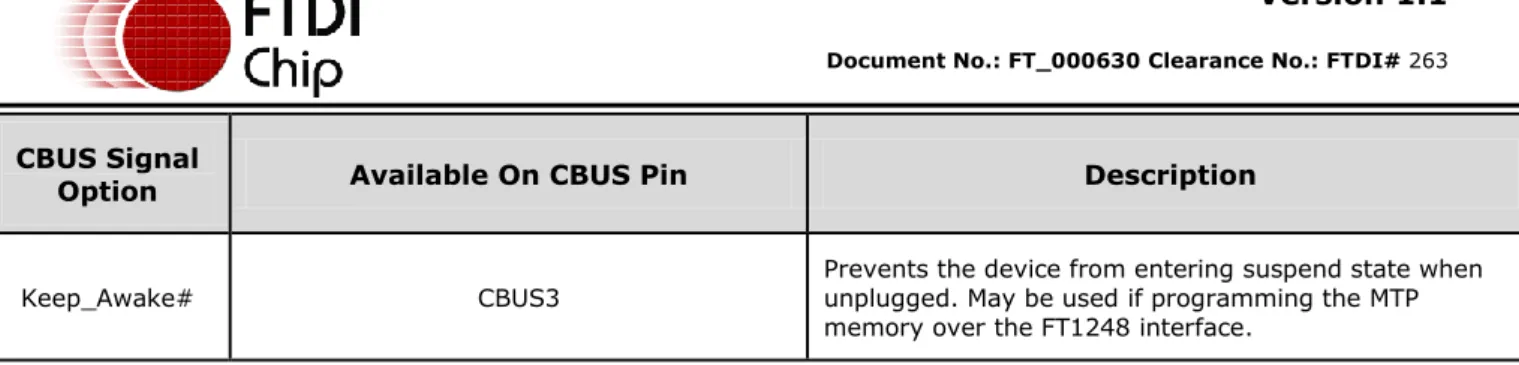
Keep_Awake# CBUS3 Prevents the device from entering suspend state when unplugged. May be used if programming the MTP memory over the FT1248 interface.
Table 3.7 CBUS Configuration Control
4
Function Description
The FT221X is a USB to FTDI Proprietary FT1248 interface device which simplifies USB implementations and reduces external component count by fully integrating into the device an MTP memory, and an integrated clock circuit which requires no external crystal. It has been designed to operate efficiently with USB host controllers by using as little bandwidth as possible when compared to the total USB bandwidth available.
4.1
Key Features
Functional Integration. Fully integrated MTP memory, USB termination resistors, clock generation, AVCC filtering, Power-On-Reset and LDO regulator.
Configurable CBUS I/O Pin Options. The fully integrated MTP memory allows configuration of the Control Bus (CBUS) functionality and drive strength selection. There is 1 configurable CBUS I/O pin. These configurable options are defined in section 3.3
The CBUS line can be configured with any one of these output options by setting bits in the internal MTP memory. The device is shipped with the most commonly used pin definitions pre-programmed - see Section 9 for details.
Asynchronous Bit Bang Mode with RD# and WR# Strobes. The FT221X supports FTDI‟s previous chip generation bit-bang mode. In bit-bang mode, the eight data lines can be switched from the regular interface mode to an 8-bit general purpose I/O port. Data packets can be sent to the device and they will be sequentially sent to the interface at a rate controlled by an internal timer (equivalent to the baud rate pre-scalar).
Synchronous Bit Bang Mode. The FT221X supports synchronous bit bang mode. This mode differs from asynchronous bit bang mode in that the interface pins are only read when the device is written to. This makes it easier for the controlling program to measure the response to an output stimulus as the data returned is synchronous to the output data. An application note, AN232R-01, available from FTDI website (www.ftdichip.com) describes this feature.
Source Power and Power Consumption. The FT221X is capable of operating at a voltage supply between +3.3V and +5.25V with a nominal operational mode current of 8mA and a nominal USB suspend mode current of 125µA. This allows greater margin for peripheral designs to meet the USB suspend mode current limit of 2.5mA. An integrated level converter within the device allows the FT221X to interface to logic running at +1.8V to +3.3V (5V tolerant).
4.2
Functional Block Descriptions
The following paragraphs detail each function within the FT221X. Please refer to the block diagram shown in Figure 2.1
Internal MTP Memory. The internal MTP memory in the FT221X is used to store USB Vendor ID (VID), Product ID (PID), device serial number, product description string and various other USB configuration descriptors. The internal MTP memory is also used to configure the CBUS pin functions. The FT221X is supplied with the internal MTP memory pre-programmed as described in Section 9. A user area of the internal MTP memory is available to system designers to allow storing additional data from the user application over USB. The internal MTP memory descriptors can be programmed in circuit, over USB without any additional voltage requirement. The descriptors can be programmed using the FTDI utility software called FT_PROG, which can be downloaded from FTDI Utilities on the FTDI website
(www.ftdichip.com). In addition to programming over USB the MTP memory may be accessed via the FT1248 interface.
+1.8V LDO Regulator. The +1.8V LDO regulator generates the +1.8V reference voltage for driving the internal core of the IC.
+3.3V LDO Regulator. The +3.3V LDO regulator generates the +3.3V reference voltage for driving the USB transceiver cell output buffers. It requires an external decoupling capacitor to be attached to the 3V3OUT regulator output pin. It also provides +3.3V power to the 1.5kΩ internal pull up resistor on USBDP. The main function of the LDO is to power the USB Transceiver and the Reset Generator Cells rather than to power external logic. However, it can be used to supply external circuitry requiring a +3.3V nominal supply with a maximum current of 50mA.
USB Transceiver. The USB Transceiver Cell provides the USB 1.1 / USB 2.0 full-speed physical interface to the USB cable. The output drivers provide +3.3V level slew rate control signalling, whilst a differential input receiver and two single ended input receivers provide USB data in, Single-Ended-0 (SE0) and USB reset detection conditions respectfully. This function also incorporates a 1.5kΩ pull up resistor on USBDP. The block also detects when connected to a USB power supply which will not enumerate the device but still supply power and may be used for battery charging.
USB DPLL. The USB DPLL cell locks on to the incoming NRZI USB data and generates recovered clock and data signals for the Serial Interface Engine (SIE) block.
Internal 12MHz Oscillator - The Internal 12MHz Oscillator cell generates a 12MHz reference clock. This provides an input to the x4 Clock Multiplier function. The 12MHz Oscillator is also used as the reference clock for the SIE, USB Protocol Engine and UART FIFO controller blocks.
Clock Multiplier / Divider. The Clock Multiplier / Divider takes the 12MHz input from the Internal Oscillator function and generates the 48MHz, 24MHz, 12MHz and 6MHz reference clock signals. The 48Mz clock reference is used by the USB DPLL and the Baud Rate Generator blocks.
Serial Interface Engine (SIE). The Serial Interface Engine (SIE) block performs the parallel to serial and serial to parallel conversion of the USB data. In accordance with the USB 2.0 specification, it performs bit stuffing/un-stuffing and CRC5/CRC16 generation. It also checks the CRC on the USB data stream.
USB Protocol Engine. The USB Protocol Engine manages the data stream from the device USB control endpoint. It handles the low level USB protocol requests generated by the USB host controller and the commands for controlling the functional parameters of the UART in accordance with the USB 2.0 specification chapter 9.
FIFO RX Buffer (512 bytes). Data sent from the USB host controller to the FT1248 interface via the USB data OUT endpoint is stored in the FIFO RX (receive) buffer. Data is removed from the buffer to the FT1248 transmit register under control of the FT1248 FIFO controller. (Rx relative to the USB interface).
FIFO TX Buffer (512 bytes). Data from the FT1248 receive register is stored in the TX buffer. The USB host controller removes data from the FIFO TX Buffer by sending a USB request for data from the device data IN endpoint. (Tx relative to the USB interface).
FT1248 interface controller. Controls the FT1248 interface, dynamically switching the width of the bus as commanded by the external bus master.
RESET Generator - The integrated Reset Generator Cell provides a reliable power-on reset to the device internal circuitry at power up. The RESET# input pin allows an external device to reset the FT221X. RESET# can be tied to VCC or left unconnected if not being used.
5
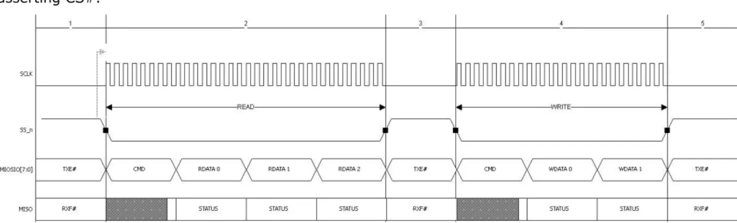
FT1248 Interface Description.
The FT1248 protocol has a dynamic bi-directional data bus interface that can be configured as 1, 2, 4, or 8-bits wide providing users with the flexibility to configure the interface with performance, pin count and PCB area in mind. For example, 1-bit mode it requires 8 clock cycles to get 8 data bits and in 8-bit mode all 8 bits are sent with one clock.
In the FT1248 there are 3 distinct phases:
While CS# is inactive, the FT1248 reflects the status of the write buffer and read buffers within the FT221X on the MIOSIO[0] and MISO wires respectively. The buffers are 512 Bytes each and the status will reflect if at least one byte of space is available for the external device to write to and whether at least one byte is available to be read by the external device.
Additionally, the FT1248 slave block supports multiple slave devices where a master can communicate with multiple SPI slave devices. When the slave is sharing buses with other SPI slave devices, the write and read buffer status cannot be reflected on the MIOSIO[0] and MISO wires during SS_n inactivity as this would cause bus contention. Therefore, it is possible for the user to select whether they wish to have the buffer status switched on or off during inactivity.
(This setting may be applied in the internal MTP memory with FT_PROG at the same time as selecting FT1248 mode).
When CS# is active a command/bus size phase occurs first. Following the command phase is the data phase, for each data byte transferred the FT1248 slave drives an ACK/NAK status onto the MISO wire. The master can send multiple data bytes so long as CS# is active, if an unsuccessful data transfer occurs, i.e. a NAK happens on the MISO wire then the master should immediately abort the transfer by de-asserting CS#.
Figure 5.1: FT1248 Basic Waveform Protocol.
5.1
Determining the Dynamic Bus Width
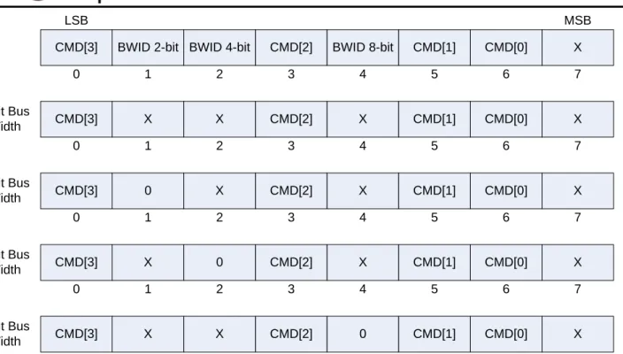
The bus width is dynamic. In order for the FT221X, in FT1248 mode, to determine the bus width within the command phase, the bus width is encoded along with the actual commands on the first active clock edge when CS# is active and has a data width of 8-bits.
If any of the MIOSIO[7:4] signals are driven low by the external host then the data transfer width equals 8-bits
If any of the MIOSIO[3:2] signals are driven low by the external host then the data transfer width equals 4-bits
If MIOSIO[1] signal is driven low by the external host then the data transfer width equals 2-bits Else the bus width is defaulted to 1-bit
In order to successfully decode the bus width, all MIOSIO signals must have pull up resistors. By default, all MIOSIO signals shall be seen by the FT221X in FT1248 mode as logic „1‟from the internal resistors. This means that when a FT1248 master does not wish to use certain MIOSIO signals, the slave (FT221X) is still capable of determining the requested bus width since any unused MIOSIO signals shall be pulled up by default.
The remaining bits used during the command phase are used to contain the command itself which means that it is possible to define up to 16 unique commands.
Figure 5.2: FT1248 Command Structure
5.2
Supported Commands on the FT1248 Interface
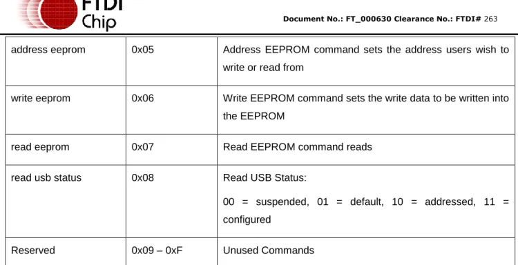
The FT1248 interface can accept and decode up to 16 unique commands. At this time only 9 unique commands are implemented as shown below.
Command Identifier Description
write 0x00 Write request command
read 0x01 Read request command
read modem status 0x02 Read modem status command, users may wish to emulate modem status control. A RMS command returns status bits RTS and DTR
write modem status 0x03 Write modem status command, users may wish to emulate modem status control. A WMS command allows users to set status bits: DCD, RI, DSR, CTS
write buffer flush 0x04 Write buffer flush request – This command is used to indicate to the FT1248 slave that its write buffers should be flushed
CMD[3] BWID 2-bit BWID 4-bit CMD[2] BWID 8-bit CMD[1] CMD[0] X
LSB MSB 0 1 2 3 4 5 6 7 1-bit Bus Width CMD[3] X X CMD[2] X CMD[1] CMD[0] X 0 1 2 3 4 5 6 7 2-bit Bus Width CMD[3] 0 X CMD[2] X CMD[1] CMD[0] X 0 1 2 3 4 5 6 7 4-bit Bus Width CMD[3] X 0 CMD[2] X CMD[1] CMD[0] X 0 1 2 3 4 5 6 7 8-bit Bus Width CMD[3] X X CMD[2] 0 CMD[1] CMD[0] X 0 1 2 3 4 5 6 7
address eeprom 0x05 Address EEPROM command sets the address users wish to write or read from
write eeprom 0x06 Write EEPROM command sets the write data to be written into the EEPROM
read eeprom 0x07 Read EEPROM command reads
read usb status 0x08 Read USB Status:
00 = suspended, 01 = default, 10 = addressed, 11 = configured
Reserved 0x09 – 0xF Unused Commands
Table 5.1: FT1248 Commands
5.3
LSB or MSB Selection
The data can be sent/received Least Significant Bit First (LSB) or Most Significant Bit First (MSB). To determine which mode is used by the FT1248 interface of the FT221X the MTP memory must be set. This may be selected with FT_PROG.
5.4
Clock Phase/Polarity
The FT1248 slave does not need to have any knowledge of clock rate as this is supplied by the FT1248 master. However the relationship between clock and data needs to be controllable, to allow the slave to operate in the same way as the master such that data is correctly driven and sampled on the correct clock phases. By configuring the polarity and phase of CLK with respect to the data it is possible to match the FT1248 master.
There are 4 possible modes which are determined by the Clock Polarity (CPOL) and Clock Phase (CPHA) signals. The different combinations of these signals are commonly referred to as modes, see Table 5.2 below. For the FT1248 slave, only 2 of these 4 modes are supported. CPHA will always be set to 1 in the FT1248 slave because data is available or driven on to MIOSIO wires on the first clock edge after CS# is active and is therefore sampled on the trailing edge of the first clock pulse. When CPHA equals 0, it means data must be available or driven onto the MIOSIO wires on the first leading edge of the clock after CS# is active. However, during this period between CS# becoming active and the first leading clock edge is when the MIOSIO wires are being “turned around” as when CS# is inactive the FT1248 slave is driving the write buffer status. Supporting CPHA = 0 would result in bus contention and therefore, shall not be supported.
Mode CPOL CPHA Supported
1 0 1 YES
2 1 0 NO
3 1 1 YES
Table 5.2: CPOL & CPHA Mode Numbers
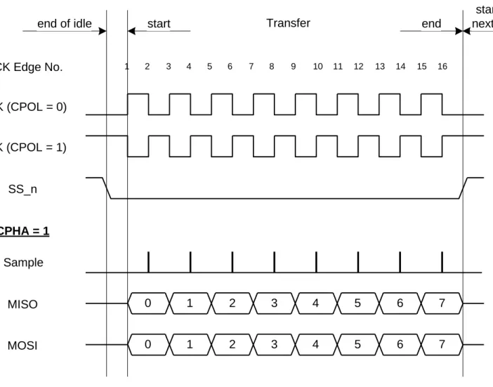
When CPOL is 1, the idle state of the clock is high. When CPOL is 0, the idle state of the clock is low. It should be noted that clock phase and polarity need to be identical for the master and attached slave device.
5.4.1
CPHA = 1
When CPHA is set to „1‟, the first edge after CS# goes low will be used to shift (or drive) the first data bit onto MIOSIO. Every odd numbered edge after this will shift out the next data bit. Incoming data will be sampled on the second or trailing SCLK edge and every even edge thereafter.
Figure 5.3 shows this for both CPOL = 0 and CPOL = 1.
Figure 5.3: FT1248 Clock Format CPHA = 1
SCK (CPOL = 0)
SCK (CPOL = 1)
start
end
SS_n
SCK Edge No.
1 2 3 4 5 6 7 8 9 10 11 12 13 14 15 16CPHA = 1
MISO
MOSI
0
1
2
3
4
5
6
7
0
1
2
3
4
5
6
7
Sample
Transfer
end of idle
start of
next idle
5.5
FT1248 Timing
Figure 5.4: FT1248 Clock Format CPHA = 1
The timings will vary depending on VCCIO.
Min (ns) Typical (ns) Max (ns) Description
T1 83.33ns SCLK Period
T2 41.67ns SCLK HIGH
T3 41.67ns SCLK LOW
T4 1 30 SCLK rising or falling driving edge to
MIOSIO/MSIO
T5 25 MIOSIO setup time to rising or falling sample
SCLK edge
T6 3 MIOSIO hold time from rising or falling sample
SCLK edge
T7 5 SS_n setup time to rising or falling SCLK edge
T8 5 SS_n hold time from rising or falling sample SCLK
edge
Table 5.3: 1V8 VCCIO timings
Min (ns) Typical (ns) Max (ns) Description
T1 83.33ns SCLK Period
T2 41.67ns SCLK HIGH
T3 41.67ns SCLK LOW
T4 1 15 SCLK rising or falling driving edge to
T5 22 MIOSIO setup time to rising or falling sample SCLK edge
T6 1 MIOSIO hold time from rising or falling sample
SCLK edge
T7 5 SS_n setup time to rising or falling SCLK edge
T8 5 SS_n hold time from rising or falling sample SCLK
edge
Table 5.4: 2V5 VCCIO timings
Min (ns) Typical (ns) Max (ns) Description
T1 83.33ns SCLK Period
T2 41.67ns SCLK HIGH
T3 41.67ns SCLK LOW
T4 1 10 SCLK rising or falling driving edge to
MIOSIO/MSIO
T5 20 MIOSIO setup time to rising or falling sample
SCLK edge
T6 0 MIOSIO hold time from rising or falling sample
SCLK edge
T7 5 SS_n setup time to rising or falling SCLK edge
T8 5 SS_n hold time from rising or falling sample SCLK
edge
6
Devices Characteristics and Ratings
6.1
Absolute Maximum Ratings
The absolute maximum ratings for the FT221X devices are as follows. These are in accordance with the Absolute Maximum Rating System (IEC 60134). Exceeding these may cause permanent damage to the device.
Parameter Value Unit Conditions
Storage Temperature -65°C to 150°C Degrees C
Floor Life (Out of Bag) At Factory Ambient (30°C / 60% Relative Humidity) 168 Hours (IPC/JEDEC J-STD-033A MSL Level 3 Compliant)* Hours
Ambient Operating Temperature (Power
Applied) -40°C to 85°C Degrees C
MTTF FT221XS TBD Hours
MTTF FT221XQ TBD Hours
VCC Supply Voltage -0.3 to +5.5 V
VCCIO IO Voltage -0.3 to +4.0 V
DC Input Voltage – USBDP and USBDM -0.5 to +3.63 V
DC Input Voltage – High Impedance
Bi-directionals (powered from VCCIO) -0.3 to +5.8 V
DC Output Current – Outputs 22 mA
Table 6.1 Absolute Maximum Ratings
* If devices are stored out of the packaging beyond this time limit the devices should be baked before use. The devices should be ramped up to a temperature of +125°C and baked for up to 17 hours.
6.2
ESD and Latch-up Specifications
Description Specification Human Body Mode (HBM) > ± 2kV
Machine mode (MM) > ± 200V Charged Device Mode (CDM) > ± 500V
Latch-up > ± 200mA
6.3
DC Characteristics
DC Characteristics (Ambient Temperature = -40°C to +85°C)
Parameter Description Minimum Typical Maximum Units Conditions
VCC VCC Operating Supply Voltage 2.97 5 5.5 V Normal Operation
VCC2 VCCIO Operating Supply Voltage 1.62 --- 3.63 V
Icc1 Operating Supply Current 8.1 11 13.1 mA Normal Operation
Icc2 Operating Supply Current 125 μA USB Suspend
3V3 3.3v regulator output 2.97 3.3 3.63 V VCC must be greater than 3V3 otherwise 3V3OUT is an input which must be driven with 3.3V
Parameter Description Minimum Typical Maximum Units Conditions
Voh Output Voltage High
2.97 VCCIO VCCIO V
Ioh = +/-2mA I/O Drive strength*
= 4mA
2.97 VCCIO VCCIO V I/O Drive strength* = 8mA
2.97 VCCIO VCCIO V I/O Drive strength* = 12mA
2.97 VCCIO VCCIO V I/O Drive strength* = 16mA
Vol Output Voltage Low
0 0.4 V
Iol = +/-2mA I/O Drive strength*
= 4mA
0 0.4 V I/O Drive strength* = 8mA
0 0.4 V I/O Drive strength* = 12mA
0 0.4 V I/O Drive strength* = 16mA
Vil Input low Switching Threshold 0.8 V LVTTL
Vih Input High Switching Threshold 2.0 V LVTTL
Vt Switching Threshold 1.49 V LVTTL
Vt- Schmitt trigger negative going threshold voltage 1.15 V
Vt+ Schmitt trigger positive going threshold voltage 1.64 V
Rpu Input pull-up resistance 40 75 190 KΩ Vin = 0
Rpd Input pull-down resistance 40 75 190 KΩ Vin =VCCIO
Iin Input Leakage Current -10 +/-1 10 μA Vin = 0
Ioz Tri-state output leakage current -10 +/-1 10 μA Vin = 5.5V or 0
Table 6.4 I/O Pin Characteristics VCCIO = +3.3V (except USB PHY pins)
Parameter Description Minimum Typical Maximum Units Conditions
Voh Output Voltage High
2.25 VCCIO VCCIO V
Ioh = +/-2mA I/O Drive strength*
= 4mA
2.25 VCCIO VCCIO V I/O Drive strength* = 8mA
2.25 VCCIO VCCIO V I/O Drive strength* = 12mA
2.25 VCCIO VCCIO V I/O Drive strength* = 16mA
Vol Output Voltage Low
0 0.4 V
Iol = +/-2mA I/O Drive strength*
= 4mA
0 0.4 V I/O Drive strength* = 8mA
0 0.4 V I/O Drive strength* = 12mA
0 0.4 V I/O Drive strength* = 16mA
Vil Input low Switching Threshold 0.8 V LVTTL
Vih Input High Switching Threshold 0.8 V LVTTL
Vt Switching Threshold 1.1 V LVTTL
Vt- Schmitt trigger negative going threshold voltage 0.8 V
Vt+ Schmitt trigger positive going threshold voltage 1.2 V
Rpu Input pull-up resistance 40 75 190 KΩ Vin = 0
Rpd Input pull-down resistance 40 75 190 KΩ Vin =VCCIO
Iin Input Leakage Current -10 +/-1 10 μA Vin = 0
Ioz Tri-state output leakage current -10 +/-1 10 μA Vin = 5.5V or 0
Table 6.5 I/O Pin Characteristics VCCIO = +2.5V (except USB PHY pins)
Parameter Description Minimum Typical Maximum Units Conditions
Voh Output Voltage High
1.62 VCCIO VCCIO V
Ioh = +/-2mA I/O Drive strength*
= 4mA
1.62 VCCIO VCCIO V I/O Drive strength* = 8mA
1.62 VCCIO VCCIO V I/O Drive strength* = 12mA
1.62 VCCIO VCCIO V I/O Drive strength* = 16mA
Vol Output Voltage Low
0 0.4 V
Iol = +/-2mA I/O Drive strength*
= 4mA
0 0.4 V I/O Drive strength* = 8mA
0 0.4 V I/O Drive strength* = 12mA
0 0.4 V I/O Drive strength* = 16mA
Vil Input low Switching Threshold 0.77 V LVTTL
Vih Input High Switching Threshold 1.6 V LVTTL
Vt Switching Threshold 0.77 V LVTTL
Vt- Schmitt trigger negative going threshold voltage 0.557 V
Vt+ Schmitt trigger positive going threshold voltage 0.893 V
Rpu Input pull-up resistance 40 75 190 KΩ Vin = 0
Rpd Input pull-down resistance 40 75 190 KΩ Vin =VCCIO
Iin Input Leakage Current -10 +/-1 10 μA Vin = 0
Ioz Tri-state output leakage current -10 +/-1 10 μA Vin = 5.5V or 0
Table 6.6 I/O Pin Characteristics VCCIO = +1.8V (except USB PHY pins)
Parameter Description Minimum Typical Maximum Units Conditions
Voh Output Voltage High VCC-0.2 V
Vol Output Voltage Low 0.2 V
Vil Input low Switching Threshold - 0.8 V
Vih Input High Switching Threshold 2.0 - V
Table 6.7 USB I/O Pin (USBDP, USBDM) Characteristics
6.4
MTP Memory Reliability Characteristics
The internal 2048 Byte MTP memory has the following reliability characteristics:
Parameter Value Unit
Data Retention 10 Years
Write Cycle 2,000 Cycles
Read Cycle Unlimited Cycles
Table 6.8 MTP Memory Characteristics
6.5
Internal Clock Characteristics
The internal Clock Oscillator has the following characteristics:
Parameter
Value
Unit
Minimum Typical Maximum
Frequency of Operation
(see Note 1) 11.98 12.00 12.02 MHz
Clock Period 83.19 83.33 83.47 ns
Duty Cycle 45 50 55 %
Table 6.9 Internal Clock Characteristics
7
USB Power Configurations
The following sections illustrate possible USB power configurations for the FT221X. The illustrations have omitted pin numbers for ease of understanding since the pins differ between the FT221XS and FT221XQ package options.
All USB power configurations illustrated apply to both package options for the FT221X device. Please refer to Section 3 for the package option pin-out and signal descriptions.
7.1
USB Bus Powered Configuration
FT221X 1 2 3 4 5 SHIELD Ferrite Bead GND GND VCC GND VCC 3V3OUT USBDM USBDP VCCIO VCC AG ND GN D RESET# 100nF 100nF 10nF 4.7uF + 27R 27R GND 47pF 47pF
Figure 7.1 Bus Powered Configuration
Figure 7.1 Illustrates the FT221X in a typical USB bus powered design configuration. A USB bus powered device gets its power from the USB bus. Basic rules for USB bus power devices are as follows –
i) On plug-in to USB, the device should draw no more current than 100mA. ii) In USB Suspend mode the device should draw no more than 2.5mA.
iii) A bus powered high power USB device (one that draws more than 100mA) should use one of the CBUS pins configured as PWREN# and use it to keep the current below 100mA on plug-in and 2.5mA on USB suspend.
iv) A device that consumes more than 100mA cannot be plugged into a USB bus powered hub. v) No device can draw more than 500mA from the USB bus.
The power descriptors in the internal MTP memory of the FT221X should be programmed to match the current drawn by the device.
A ferrite bead is connected in series with the USB power supply to reduce EMI noise from the FT221X and associated circuitry being radiated down the USB cable to the USB host. The value of the Ferrite Bead depends on the total current drawn by the application. A suitable range of Ferrite Beads is available from Steward (www.steward.com), for example Steward Part # MI0805K601R-10.
FT221X 1 2 3 4 5 SHIELD GND GND VCC GND VCC 3V3OUT USBDM USBDP VCCIO VCC(3.3-5.25V) AG ND GN D RESET# 100nF 100nF 100nF 4.7uF + GND 4k7 10k 27R 27R 47pF 47pF GND VBUS_SENSE
Figure 7.2 Self Powered Configuration
Figure 7.2 illustrates the FT221X in a typical USB self powered configuration. A USB self powered device gets its power from its own power supply, VCC, and does not draw current from the USB bus. The basic rules for USB self powered devices are as follows –
i) A self powered device should not force current down the USB bus when the USB host or hub controller is powered down.
ii) A self powered device can use as much current as it needs during normal operation and USB suspend as it has its own power supply.
iii) A self powered device can be used with any USB host, a bus powered USB hub or a self powered USB hub.
The power descriptor in the internal MTP memory of the FT221X should be programmed to a value of zero (self powered).
In order to comply with the first requirement above, the USB bus power (pin 1) is used to control the VBUS_Sense pin of the FT221X device. When the USB host or hub is powered up an internal 1.5kΩ resistor on USBDP is pulled up to +3.3V, thus identifying the device as a full speed device to the USB host or hub. When the USB host or hub is powered off, VBUS_Sense pin will be low and the FT221X is held in a suspend state. In this state the internal 1.5kΩ resistor is not pulled up to any power supply (hub or host is powered down), so no current flows down USBDP via the 1.5kΩ pull-up resistor. Failure to do this may cause some USB host or hub controllers to power up erratically.
Figure 7.2 illustrates a self powered design which has a +3.3V to +5.25V supply. Note:
1. When the FT221X is in reset, the UART interface I/O pins are tri-stated. Input pins have internal 200kΩ pull-up resistors to VCCIO, so they will gently pull high unless driven by some external logic.
7.3
USB Bus Powered with Power Switching Configuration
FT221X 1 2 3 4 5 SHIELD Ferrite Bead GND GND VCC GND VCC 3V3OUT USBDM USBDP VCCIO AG ND GN D RESET# 100nF 100nF 10nF 4.7uF + CBUS3 PWREN# 10k 1k Switched 5V Power to External Logic 0.1uF 0.1uF P Channel Power MOSFET 27R 27R GND 47pF 47pFFigure 7.3 Bus Powered with Power Switching Configuration
A requirement of USB bus powered applications, is when in USB suspend mode, the application draws a total current of less than 2.5mA. This requirement includes external logic. Some external logic has the ability to power itself down into a low current state by monitoring the PWREN# signal. For external logic that cannot power itself down in this way, the FT221X provides a simple but effective method of turning off power during the USB suspend mode.
Figure 7.3 shows an example of using a discrete P-Channel MOSFET to control the power to external logic. A suitable device to do this is an International Rectifier (www.irf.com) IRLML6402, or equivalent. It is recommended that a “soft start” circuit consisting of a 1kΩ series resistor and a 0.1μF capacitor is used to limit the current surge when the MOSFET turns on. Without the soft start circuit it is possible that the transient power surge, caused when the MOSFET switches on, will reset the FT221X or the USB host/hub controller. The soft start circuit example shown in Figure 7.3 powers up with a slew rate of
approximaely12.5V/ms. Thus supply voltage to external logic transitions from GND to +5V in approximately 400 microseconds.
As an alternative to the MOSFET, a dedicated power switch IC with inbuilt “soft-start” can be used. A suitable power switch IC for such an application is the Micrel (www.micrel.com) MIC2025-2BM or equivalent.
With power switching controlled designs the following should be noted:
i) The external logic to which the power is being switched should have its own reset circuitry to automatically reset the logic when power is re-applied when moving out of suspend mode. ii) Set the Pull-down on Suspend option in the internal FT221X MTP memory.
iii) One of the CBUS Pins should be configured as PWREN# in the internal FT221X MTP memory, and used to switch the power supply to the external circuitry.
iv) For USB high-power bus powered applications (one that consumes greater than 100mA, and up to 500mA of current from the USB bus), the power consumption of the application must be set in the Max Power field in the internal FT221X MTP memory. A high-power bus powered application uses the descriptor in the internal FT221X MTP memory to inform the system of its power requirements.
v) PWREN# gets its VCC from VCCIO. For designs using 3V3 logic, ensure VCCIO is not powered down using the external logic. In this case use the +3V3OUT.
7.4
USB Battery Charging Detection
A recent addition to the USB specification (http://www.usb.org/developers/devclass_docs/BCv1.2_011912.zip ) is to allow for additional charging profiles to be used for charging batteries in portable devices. These charging profiles do not enumerate the USB port of the peripheral. The FT221X device will detect that a USB compliant dedicated charging port (DCP) is connected. Once detected while in suspend mode a battery charge detection signal is provided to allow external logic to switch to charging mode as opposed to operation mode.
X-Chip Pin Function
EEPROM Setting
CBUS3 BCD
Battery Options Battery Charger Enable
Force Power Enable De-acticate Sleep X GND GND 0.1uF 0.1uF GND GND 600R/2A 10nF VBUS 3V3OUT 0.1uF 0R GND SLD GND 27R 27R VBUS 1 D- 2 D+ 3 GND 5 ID 4 CN USB VCC 2 FAULT 3 TIMER 4 GND 5 NTC 6 PROG 7 SHDN 8 BAT 9 ACPR 10 CHRG 1 G N D 1 1 LTC4053EDD GND 3V3OUT 3V3OUT 4.7uF 0.1uF GND VBUS VBUS GND VBATT GND GND 1K5 GND 1 TB3.5mm VBUS VBUS NTC 0.1uF GND VBUS 1uF 1R GND VBUS BCD 2K2 GND JP1 1-2 2-3 NCT Enabled NCT Available JP1 SIP-3 NTC GND NCT Disabled (Default) JUMPER-2mm 4K32 1% G N D DP DM 3V3OUT RESET# V C C G N D CBUS3 V C C IO FT221X BCD
1A when connected to a dedicated charger port 0A when enumerated
0A when in sleep
0A when not enumerated and not in sleep + -NCT N.F.
Figure 7.4 USB Battery Charging Detection
To use the FT221X with battery charging detection the CBUS pin must be reprogrammed to allow for the BCD Charger output to switch the external charger circuitry on. The CBUS pins are configured in the internal MTP memory with the free utility FTPROG. If the charging circuitry requires an active low signal
For more configuration options of the LTC4053 refer to: AN_175_Battery Charging Over USB
8
Application Examples
The following sections illustrate possible applications of the FT221X. The illustrations have omitted pin numbers for ease of understanding since the pins differ between the FT221XS and FT221XQ package options.
8.1
USB to FT1248 Converter
Figure 8.1 Application Example showing USB to FT1248 host
NOTE: ALL IO LINES SHOULD HAVE A 10k PULL UP TO VCCIO
The FT1248 can be used with 1-bit, 2-bit, 4-bit or 8-bit wide data. The Figure 8.1 is showing 8 bit mode. By using 8 data bits you need fewer clock cycles to get the data across.
The FT221X is the slave device and the external FPGA/MCU is the bus master. The FT221X will auto detect the bus width from the initial command byte sent by the controller. If not using all 8 data lines the pins may be left unterminated as an internal pull-up ensures the device detects a logic 1.
Timing diagrams for 8-bit accesses can be seen in figures 8.2 and 8.3. For further information on the mode see AN_167 FT1248 Basics from the FTDI website.
BUS TURNAROUND WRITE DATA 1 COMMAND PHASE BUS TURNAROUND TXE# CMD3 0 CMD2 B7 B6 B5 B4 B7 B6 B5 B4 TXE# CLK SS_n MIOSIO[0] RXF# MISO MIOSIO[4] TXE# ACK RXF# BUS TURNAROUND MIOSIO[1] 0 MIOSIO[2] MIOSIO[3] 0 B3 B3 CMD0 B2 B1 B2 B1 CMD1 X B0 B0 MIOSIO[5] MIOSIO[6] MIOSIO[7] ACK
READ DATA 2 READ DATA 1 COMMAND PHASE BUS TURNAROUND TXE# CMD3 0 CMD2 B7 B6 B5 B4 B7 B6 B5 B4 TXE# CLK SS_n MIOSIO[0] RXF# MISO MIOSIO[4] RXF# ACK RXF# BUS TURNAROUND MIOSIO[1] 0 MIOSIO[2] MIOSIO[3] 0 B3 B3 CMD0 B2 B1 B2 B1 CMD1 X B0 B0 MIOSIO[5] MIOSIO[6] MIOSIO[7] ACK
8.2
LED Interface
Any of the CBUS I/O pins can be configured to drive an LED. The FT221X has 3 configuration options for driving LEDs from the CBUS. These are TXLED#, RXLED#, and TX&RXLED#. Refer to Section 0 for configuration options.
FT221X
CBUS[3] TX& RXLED#
270R VCCIO
LED
Figure 8.4 Single LED Configuration
An example of using the FT221X to drive LEDs is shown in Figure 8.4. In this example one of the CBUS pins is used to indicate when data is being transmitted or received by the device (TX&RXLED). In this configuration the FT221X will drive only a single LED.
9
Internal MTP Memory Configuration
The FT221X includes an internal MTP memory which holds the USB configuration descriptors, other configuration data for the chip and also user data areas. Following a power-on reset or a USB reset the FT221X will scan its internal MTP memory and read the USB configuration descriptors stored there. In many cases, the default values programmed into the MTP memory will be suitable and no re-programming will be necessary. The defaults can be found in Section 9.1.
The MTP memory in the FT221X can be programmed over USB or over the FT1248 bus if the values need to be changed for a particular application. Further details of this are provided from section 9.2 onwards. Users who do not have their own USB Vendor ID but who would like to use a unique Product ID in their design can apply to FTDI for a free block of unique PIDs. See TN_100 – USB Vendor ID/Product ID Guidelines for more details.
9.1
Default Values
The default factory programmed values of the internal MTP memory are shown in Table 9.1.
Parameter Value Notes
USB Vendor ID (VID) 0403h FTDI default VID (hex)
USB Product UD (PID) 6015h FTDI default PID (hex)
Serial Number Enabled? Yes
Serial Number See Note programmed into the MTP memory during device A unique serial number is generated and final test.
Pull down I/O Pins in USB
Suspend Disabled
Enabling this option will make the device pull down on the UART interface lines when in USB suspend
mode (PWREN# is high).
Manufacturer Name FTDI
Product Description FT221X 8-BIT FT1248 Max Bus Power Current 90mA
Power Source Bus Powered
Device Type FT221X
USB Version 0200
Returns USB 2.0 device description to the host. Note: The device is a USB 2.0 Full Speed device
Parameter Value Notes
DBUS Schmitt Trigger
Enable Normal Options are normal or Schmitt
CBUS Drive Current
Strength 4mA Options are 4mA, 8mA, 12mA, 16mA
CBUS slew rate Slow Options are slow or fast
CBUS Schmitt Trigger
Enable Normal Options are normal or Schmitt
Load VCP Driver Disabled Enabling this will load the VCP driver interface for the device.
CBUS3 Keep_Awake#
Prevents the device from entering suspend state when unplugged. May be used if programming the
MTP memory over the FT1248 interface.
Table 9.1 Default Internal MTP Memory Configuration
9.2
Methods of Programming the MTP Memory
9.2.1
Programming the MTP memory over USB
The MTP memory on all FT-X devices can be programmed over USB. This method is the same as for the EEPROM on other FTDI devices such as the FT232R. No additional hardware, connections or programming voltages are required. The device is simply connected to the host computer in the same way that it would be for normal applications, and the FT_Prog utility is used to set the required options and program the device.
The FT_Prog utility is provided free-of-charge from the FTDI website, and can be found at the link below. The user guide is also available at this link.
http://www.ftdichip.com/Support/Utilities.htm#FT_Prog
Additionally, D2XX commands can be used to program the MTP memory from within user applications. For more information on the commands available, please see the D2XX Programmers Guide below.
http://www.ftdichip.com/Support/Documents/ProgramGuides/D2XX_Programmer's_Guide(FT_000071).p df
9.2.2
Programming the MTP memory over FT1248
In the FT221X device, it is possible to program the MTP memory over its FT1248 interface. This is the same interface which is used in the normal application of the FT221X and would normally be connected to a microcontroller (MCU) or FPGA. However, special commands can also be used to access the MTP
memory in the FT221X over the same FT1248 connection, allowing the MCU/FPGA to read and write locations in the MTP memory. No additional hardware, connections or programming voltages are required.
Two examples where it may be desired to use the FT1248 interface to write and read the MTP Memory are given below. In some cases, the application may use both of these possibilities.
1. To store and retrieve application specific data such as calibration constants in the user area (e.g. if the overall application was an analog measurement system). This can avoid the need for an extra EEPROM chip on the application board.
2. To read and write the configuration data (e.g. custom VID, PID, description strings or CBUS signal selection to enable signals for battery charging etc) without a USB host. This could allow an MCU/FPGA to configure the FT221X during production testing of the finished device or even when in use in the field.
The information in the rest of this chapter can be used to implement the storing and reading of
application data in the user area as in example 1 above. Example 2 requires details of the configuration data stored in the MTP memory which is FTDI proprietary information. A separate application note is available under NDA from FTDI support for customers who require to do this ([email protected]).
9.3
Memory Map
The FT-X family MTP memory has various areas which come under three main categories: User Memory Area
Configuration Memory Area (writable) Configuration Memory Area (non-writable)
Memory Area Description
Word Address
User Memory Area 2
Accessible via USB, I
2C and FT1248
0x3FF - 0x80
Configuration Memory Area
Accessible via USB, I
2C and FT1248
0x7E - 0x50
Configuration Memory Area
Cannot be written
0x4E - 0x40
User Memory Area 1
Accessible via USB, I
2C and FT1248
0x3E - 0x12
Configuration Memory Area
Accessible via USB, I
2C and FT1248
0x10 - 0x00
Figure 9.1: Simplified memory map for the FT-X
User Memory Area
The User Memory Areas are highlighted in Green on the memory map. They can be read and written via both USB and FT1248 on the FT221X. All locations within this range are freely programmable; no areas have special functions and there is no checksum for the user area.
Note that the application should take into account the specification for the number of write cycles in Section 6.4 if it will be writing to the MTP memory multiple times.
This area is included in a checksum which covers configuration areas of the memory, and so changing any value can also cause this checksum to fail.
Configuration Memory Area (non-writable)
This is a reserved area and the application should not write to this area of memory. Any attempt to write these locations will fail.
9.4
Hardware Requirements
The hardware is the same as for a typical USB-FT1248 application and no additional hardware or
programming voltages are required. The FT1248 connections are the same as shown in Section 5. For the USB connections, either a bus-powered configuration (see Section 7.1 and 7.3) or a self-powered
configuration (see Section 7.2) could be used.
9.5
Protocol
The FT1248 MTP memory protocol consists of 3 commands: Address MTP memory (0x05)
Write MTP memory (0x06) Read MTP memory (0x07)
For further details on the FT1248 protocol, refer to section 5.
9.5.1
Address MTP memory (0x05)
This consists of a command phase followed by 2 data bytes which represent the MTP memory address allowing users to address, potentially, up to 64K byte addresses.
9.5.2
Write MTP memory (0x06)
This consists of a command phase followed by 1 data byte which shall be programmed into the MTP memory at the address location set by the MTP memory address command.
9.5.3
Read MTP memory (0x07)
This consists of a command phase followed by 1 data byte which is the data read from the MTP memory at the address location set by the MTP memory address command.
9.5.4
Examples of Writing and Reading
When performing MTP memory write and read requests via the FT1248 protocol, users must first issue the MTP memory address command along with 2 bytes representing the MTP memory address. The status and acknowledge phases of this command represents the current status of the MTP memory (whether it is busy or not). If the MTP memory is being accessed during an FT1248 access then the status and acknowledge of the respective command and data phases will NAK the master. The address will only be updated when the MTP memory is inactive.
Writing
The first part of the communication sets the address, and this is followed by the write command along with the data to be written. The MTP memory write itself will be initiated when the FT221X receives an MTP memory write command followed by a single data byte. Two status phases occur during an MTP write (once during the command phase and the other during the data phase). Both status phases represent the current activity of the MTP memory (busy or not busy). A successful write will only occur when both status phases acknowledge the master indicating that the MTP memory can start the write. Users wishing to determine if the MTP memory write was successful should immediately try an EEPROM read.
Reading
As with the writing process, the first part of the communication for a read sets the address. The read will then be initiated when the FT1248 slave receives an MTP memory read command. The status during the command phase indicates whether or not the MTP memory shall be able to service the read request. If it is possible to carry out the read, the FT1248 moves into the data phase where it can either continue with the read transaction until the slave successfully returns an ACK along with the data or if it receives NAK during the data phase it can abort the read transfer and try again. When the read has been serviced the data shall be returned on the 1st data byte phase.
10
Package Parameters
The FT221X is available in two different packages. The FT221XS is the SSOP-20 option and the FT221XQ is the QFN-32 package option. The solder reflow profile for both packages is described in Section 10.5.
10.1
SSOP-20 Package Mechanical Dimensions
Figure 10.1 SSOP-20 Package Dimensions
The FT221XS is supplied in a RoHS compliant 20 pin SSOP package. The package is lead (Pb) free and uses a „green‟ compound. The package is fully compliant with European Union directive 2002/95/EC. This package is nominally 8.66mm x 3.91mm body (8.66mm x 5.99mm including pins). The pins are on a 0.635 mm pitch. The above mechanical drawing shows the SSOP-20 package.
10.2
SSOP-20 Package Markings
Figure 10.2 QFN-20 Package Markings
The date code format is YYXX where XX = 2 digit week number, YY = 2 digit year number. This is followed by the revision number.
The code XXXXXXXXXXXX is the manufacturing LOT code.
FT221XS
1
10
11
20
10.3
QFN-20 Package Mechanical Dimensions
Figure 10.3 QFN-20 Package Dimensions
The FT221XQ is supplied in a RoHS compliant leadless QFN-20 package. The package is lead (Pb) free, and uses a „green‟ compound. The package is fully compliant with European Union directive 2002/95/EC. This package is nominally 4.00mm x 4.00mm. The solder pads are on a 0.50mm pitch. The above mechanical drawing shows the QFN-32 package. All dimensions are in millimetres.
The centre pad on the base of the FT221XQ is internally connected to GND, and the PCB should not have signal tracks on the top layer under this device.
10.4
QFN-20 Package Markings
Figure 10.4 QFN-20 Package Markings
The date code format is YYXX where XX = 2 digit week number, YY = 2 digit year number. This is followed by the revision number.
The code XXXXXXX is the manufacturing LOT code.
FTDI
I
XXXXXXXXXX
FT221XQ
6 1YYWW-B
10 15 2010.5
Solder Reflow Profile
The FT221X is supplied in Pb free 20 LD SSOP and QFN-20 packages. The recommended solder reflow profile for both package options is shown in Figure 10.5.
Figure 10.5 FT221X Solder Reflow Profile
The recommended values for the solder reflow profile are detailed in Table 10.1. Values are shown for both a completely Pb free solder process (i.e. the FT221X is used with Pb free solder), and for a non-Pb free solder process (i.e. the FT221X is used with non-Pb free solder).
Profile Feature Pb Free Solder Process Non-Pb Free Solder Process
Average Ramp Up Rate (Ts to Tp) 3°C / second Max. 3°C / Second Max.
Preheat
- Temperature Min (Ts Min.)
- Temperature Max (Ts Max.)
- Time (ts Min to ts Max)
150°C 200°C 60 to 120 seconds 100°C 150°C 60 to 120 seconds Time Maintained Above Critical Temperature
TL: - Temperature (TL) - Time (tL) 217°C 60 to 150 seconds 183°C 60 to 150 seconds Peak Temperature (Tp) 260°C 240°C
Time within 5°C of actual Peak Temperature (tp)
20 to 40 seconds 20 to 40 seconds
Ramp Down Rate 6°C / second Max. 6°C / second Max.
Time for T= 25°C to Peak Temperature, Tp 8 minutes Max. 6 minutes Max.
Table 10.1 Reflow Profile Parameter Values
Critical Zone: when T is in the range T to T
T
e
m
p
e
ra
tu
re
,
T
(
D
e
g
re
e
s
C
)
Time, t (seconds)
25 P T = 25º C to T tp Tp TL t PreheatS tL Ramp Up L p Ramp Down T MaxS T MinS11
Contact Information
Head Office – Glasgow, UKFuture Technology Devices International Limited Unit 1, 2 Seaward Place, Centurion Business Park Glasgow G41 1HH
United Kingdom
Tel: +44 (0) 141 429 2777 Fax: +44 (0) 141 429 2758
E-mail (Sales) [email protected]
E-mail (Support) [email protected]
E-mail (General Enquiries) [email protected]
Branch Office – Taipei, Taiwan
Future Technology Devices International Limited (Taiwan)
2F, No. 516, Sec. 1, NeiHu Road Taipei 114
Taiwan , R.O.C.
Tel: +886 (0) 2 8791 3570 Fax: +886 (0) 2 8791 3576
E-mail (Sales) [email protected]
E-mail (Support) [email protected]
E-mail (General Enquiries) [email protected]
Branch Office – Hillsboro, Oregon, USA
Future Technology Devices International Limited (USA)
7235 NW Evergreen Parkway, Suite 600 Hillsboro, OR 97123-5803
USA
Tel: +1 (503) 547 0988 Fax: +1 (503) 547 0987
E-Mail (Sales) [email protected]
E-Mail (Support) [email protected]
E-Mail (General Enquiries) [email protected]
Branch Office – Shanghai, China
Future Technology Devices International Limited (China)
Room 408, 317 Xianxia Road, Shanghai, 200051
China
Tel: +86 21 62351596 Fax: +86 21 62351595
E-mail (Sales) [email protected]
E-mail (Support) [email protected]
E-mail (General Enquiries) [email protected]
Web Site
http://ftdichip.com
System and equipment manufacturers and designers are responsible to ensure that their systems, and any Future Technology Devices International Ltd (FTDI) devices incorporated in their systems, meet all applicable safety, regulatory and system-level performance requirements. All application-related information in this document (including application descriptions, suggested FTDI devices and other materials) is provided for reference only. While FTDI has taken care to assure it is accurate, this information is subject to customer confirmation, and FTDI disclaims all liability for system designs and for any applications assistance provided by FTDI. Use of FTDI devices in life support and/or safety applications is entirely at the user‟s risk, and the user agrees to defend, indemnify and hold harmless FTDI from any and all damages, claims, suits or expense resulting from such use. This document is subject to change without notice. No freedom to use patents or other intellectual property rights is implied by the publication of this document. Neither the whole nor any part of the information contained in, or the product described in this document, may be adapted or reproduced in any material or electronic form without the prior written consent of the copyright holder. Future Technology Devices International Ltd, Unit 1, 2 Seaward Place, Centurion Business Park,
Appendix A – References
Useful Application Noteshttp://www.ftdichip.com/Documents/AppNotes/AN232R-01_FT232RBitBangModes.pdf http://www.ftdichip.com/Documents/AppNotes/AN_107_AdvancedDriverOptions_AN_000073.pdf http://www.ftdichip.com/Documents/AppNotes/AN_121_FTDI_Device_EEPROM_User_Area_Usage.pdf http://www.ftdichip.com/Documents/AppNotes/AN_167_FT1248_Parallel_Serial_Interface_Basics.pdf http://www.ftdichip.com/Documents/InstallGuides.htm http://www.ftdichip.com/Support/Documents/TechnicalNotes/TN_100_USB_VID-PID_Guidelines.pdf http://www.ftdichip.com/Support/Documents/AppNotes/AN_175_Battery%20Charging%20Over%20USB %20with%20FTEX%20Devices.pdf http://www.usb.org/developers/devclass_docs/BCv1.2_011912.zip
Appendix B - List of Figures and Tables
List of FiguresFigure 2.1 FT221X Block Diagram ... 4
Figure 3.1 QFN Schematic Symbol ... 7
Figure 3.2 SSOP Schematic Symbol ... 9
Figure 5.1: FT1248 Basic Waveform Protocol. ... 15
Figure 5.2: FT1248 Command Structure ... 16
Figure 5.3: FT1248 Clock Format CPHA = 1 ... 18
Figure 5.4: FT1248 Clock Format CPHA = 1 ... 19
Figure 7.1 Bus Powered Configuration ... 27
Figure 7.2 Self Powered Configuration ... 28
Figure 7.3 Bus Powered with Power Switching Configuration ... 29
Figure 7.4 USB Battery Charging Detection ... 30
Figure 8.1 Application Example showing USB to FT1248 host ... 32
Figure 8.2 FT1248 8- bit write timing diagram ... 33
Figure 8.3 FT1248 8- bit read timing diagram ... 34
Figure 8.4 Single LED Configuration ... 35
Figure 9.1: Simplified memory map for the FT-X ... 38
Figure 10.1 SSOP-20 Package Dimensions ... 41
Figure 10.2 QFN-20 Package Markings ... 42
Figure 10.3 QFN-20 Package Dimensions ... 43
Figure 10.4 QFN-20 Package Markings ... 44
Figure 10.5 FT221X Solder Reflow Profile ... 45
List of Tables Table 3.1 Power and Ground ... 7
Table 3.2 Common Function pins ... 8
Table 3.3 FT1248 Interface and CBUS Group (see note 1)... 8
Table 3.4 Power and Ground ... 9
Table 3.5 Common Function pins ... 9
Table 3.6 FT1248 Interface and CBUS Group (see note 1)... 10
Table 3.7 CBUS Configuration Control ... 12
Table 5.1: FT1248 Commands ... 17
Table 5.2: CPOL & CPHA Mode Numbers ... 18
Table 5.3: 1V8 VCCIO timings ... 19
Table 6.6 I/O Pin Characteristics VCCIO = +1.8V (except USB PHY pins) ... 25
Table 6.7 USB I/O Pin (USBDP, USBDM) Characteristics ... 26
Table 6.8 MTP Memory Characteristics ... 26
Table 6.9 Internal Clock Characteristics ... 26
Table 9.1 Default Internal