I
DYNAMIC POWER CONSUMPTION ESTIMATION AND REDUCTION FOR FULL SEARCH MOTION ESTIMATION HARDWARE
by
ÇAĞLAR KALAYCIOĞLU
Submitted to the Graduate School of Engineering and Natural Sciences in partial fulfillment of
the requirements for the degree of Master of Science
Sabancı University Spring 2009
II
DYNAMIC POWER CONSUMPTION ESTIMATION AND REDUCTION FOR FULL SEARCH MOTION ESTIMATION HARDWARE
APPROVED BY:
Assist. Prof. Dr. İlker Hamzaoğlu ………. (Thesis Supervisor)
Prof. Dr. Ahmet Oral ……….
Assist. Prof. Dr. Ahmet Onat ……….
Assist. Prof. Dr. Hüsnü Yenigün ……….
Assist. Prof. Dr. Hakan Erdoğan ……….
III
© Çağlar Kalaycıoğlu 2009 All Rights Reserved
IV
DYNAMIC POWER CONSUMPTION ESTIMATION AND REDUCTION FOR FULL SEARCH MOTION ESTIMATION HARDWARE
Çağlar Kalaycıoğlu EE, Master Thesis, 2009
Thesis Supervisor: Assist. Prof. Dr. İlker Hamzaoğlu
ABSTRACT
Motion Estimation (ME) is the most computationally intensive and most power consuming part of video compression and video enhancement systems. ME is used in video compression standards such as MPEG4, H.264 and it is used in video enhancement algorithms such as frame rate conversion and de-interlacing. Since portable devices operate with battery, it is important to reduce power consumption so that the battery life can be increased. In addition, consuming excessive power degrades the performance of integrated circuits, increases packaging and cooling costs, reduces the reliability and may cause device failures. Therefore, estimating and reducing power consumption of motion estimation hardware is very important.
In this thesis, we propose a novel dynamic power estimation technique for full search ME hardware. We estimated the power consumption of two full search ME hardware implementations on a Xilinx Virtex II FPGA using several existing high and low level dynamic power estimation techniques and our technique. Gate-level timing simulation based power estimation of full search ME hardware for an average frame using Xilinx XPower tool takes 6 - 18 hours in a state-of-the-art PC, whereas estimating the power consumption of the same ME hardware for the same frame takes a few seconds using our technique. The average and maximum difference between the power consumptions estimated by our technique and the power consumptions estimated by XPower tool for four different video sequences are %3 and %13 respectively.
V
We also propose a novel dynamic power reduction technique for ME hardware. We quantified the impact of glitch reduction, clock gating and the proposed technique on the power consumption of two full search ME hardware implementations on a Xilinx Virtex II FPGA using Xilinx XPower tool. Glitch reduction and clock gating together achieved an average of 21% dynamic power reduction. The proposed technique achieved an average of 23% dynamic power reduction with an average of 0.4dB PSNR loss. The proposed technique achieves better power reduction than pixel truncation technique with a similar PSNR loss.
We also showed that our dynamic power estimation technique can be used for developing novel dynamic power reduction techniques. To do this, we used our technique to estimate the dynamic power consumption of the ME hardware when two different dynamic power reduction techniques are used. The results show that if a power reduction technique only changes the input data order of the ME hardware, the proposed dynamic power estimation technique can be used to quickly estimate the effectiveness of that technique. However, if the architecture of the ME hardware is modified, the accuracy of the power consumption estimations decrease. Therefore the proposed power estimation technique should be improved for this case.
VI
TAM ARAMA HAREKET TAHMİNİ DEVRELERİNDE DİNAMİK GÜÇ TÜKETİMİ TAHMİNİ VE AZALTILMASI
Çağlar Kalaycıoğlu EE, Yüksek Lisans Tezi, 2009
Tez Danışmanı: Yard. Doç. Dr. İlker Hamzaoğlu
ÖZET
Hareket Tahmini (HT) video sıkıştırma ve video iyileştirme işlemlerini yapan sistemlerin en çok güç harcayan kısmıdır. HT, MPEG4 ve H.264 gibi video sıkıştırma standartlarında ve çerçeve hızı dönüştürme gibi video iyileştirme işlerinde kullanılır. Taşınabilir cihazlar pil ile çalıştığı için, güç tüketimini azaltmak pil ömrünün uzamasını
sağlayacaktır. Bunun yanında aşırı güç tüketimi, entegre devrelerin performansını düşürür, paketleme ve soğutma maliyetlerini arttırır, dayanıklılığını azaltır ve bozulmalarına sebep olabilir. Bu nedenle, güç tüketiminin tahmini ve azaltılması, HT donanımı tasarım akışının önemli bir parçasıdır.
Bu tezde, HT donanımı için yeni bir dinamik güç tahmin tekniği önerildi. Çeşitli yüksek ve düşük seviye güç tahmin tekniklerinin ve önerilen yeni tekniğin etkisi nicelendi. Önerilen tekniğin, dört farklı video dizisi için, çok yüksek hassaslığa sahip olan Xilinx XPower programının tahmin sonuçları ile ortalama farkının %3 olduğu, maksimum farkının ise %13 olduğu görüldü. XPower kullanılarak bir video çerçevesi işleyen bir HT devresinin güç tahmininin yapılması en son teknoloji ürünü bir kişisel bilgisayarda 6-18 saat sürmektedir. Bu göz önüne alındığında birkaç saniye içinde %3 fark ile ortalama bir video çerçevesi için güç tahmini yapabilmek büyük bir ilerleme sayılabilir.
VII
Ayrıca bu tezde, HT devreleri için yeni bir dinamik güç tüketimi azaltma yöntemi önerildi. Küçük sıçramaları azaltma, saat kapılama ve yeni önerilen tekniğin Xilinx Virtex II FPGA üzerinde gerçekleştirilen iki farklı HT devresine olan etkileri Xilinx XPower programı
ile belirlendi. Küçük sıçramaları azaltma ve saat kapılama yöntemleri tüketilen dinamik gücü %21 düşürdü. Ayrıca önerilen yeni dinamik güç azaltma tekniği sadece 0.4dB kalite kaybı ile ortalama gücü %23 düşürdü. Bu teknik piksel kırpma tekniği ile karşılaştırıldı ve benzer kalite kaybı değerlerinde daha çok güç azaltımı sağladığı görüldü.
Daha sonra, önerilen yeni dinamik güç tahmin tekniğinin, yeni dinamik güç azaltma tekniklerinin geliştirilmesinde kullanılabileceği gösterildi. Bunu yapmak için yeni dinamik güç tahmin tekniği, iki farklı dinamik güç azaltma tekniğinin kullanıldığı HT devrelerinin dinamik güç tahminlerini yapmak için kullanıldı. Sonuçlar dinamik güç azaltma tekniği eğer giriş verilerinin sıralamasını değiştiriyorsa, HT donanımının harcadığı dinamik gücün yüksek hassasiyet ile tahmin edilebildiğini gösterdi. Fakat güç azaltma tekniği bir mimari değişikliğe yol açıyorsa, HT donanımının harcadığı gücün daha düşük bir hassasiyet ile tahmin edilebildiğini ve önerilen tekniğin bu durum için daha iyileştirilmesinin gerektiğini gösterdi.
VIII
IX
ACKNOWLEDGEMENTS
First and foremost, I would like to thank my advisor, Assist. Prof. Dr. İlker Hamzaoğlu, for his assistance, guidance and patience. For years he has guided me in developing my ideas, tracked the development of my thesis and shared his knowledge.
Second, my thanks go to my fellow “System-on-a-Chip Lab” mates; Merve, Onur, Yusuf, Mustafa, Mert, Kadir, Aydın, Murat and Özgür. Although we sometimes triggered each other to procrastinate, most of the time we kept each others’ morale up and never let the lab become a boring place. I’ll miss you guys.
My acknowledgements also go to Sabancı University and TÜBİTAK for supporting me with scholarships during my Master of Science study.
I also would like to express my deepest gratitude to my parents, my mother Mahinur and my father Haluk. They worked tirelessly for the well being of their only son and supported me wherever they can. It is very heartwarming to know that one has such parents.
Last but not the least; I want to thank my love, Berrak Can Çivili. “You are my other half and I want to be with you forever!”
X TABLE OF CONTENTS 1 ABSTRACT………..………IV 2 ÖZET………VI 3 ACKNOWLEDGEMENTS………..IV 4 TABLE OF CONTENTS………...X 6 LIST OF FIGURES……….XII 7 LIST OF TABLES……….XIV 8 ABBREVIATIONS……….XV 1 CHAPTER I………1 INTRODUCTION……….………..1 2 CHAPTER II……….………..5
FULL SEARCH MOTION ESTIMATION HARDWARE DESIGNS………...5
2.1 Full Search Motion Estimation Algorithm………..5
2.2 16 Processing Element Fixed Block Size Motion Estimation Hardware………7
2.3 256 Processing Element Variable Block Size Motion Estimation Hardware…...……10
3 CHAPTER III………16
DYNAMIC POWER ESTIMATION OF MOTION ESTIMATION HARDWARE...16
3.1 High Level Dynamic Power Estimation……….………...16
XI
3.3 A Novel Dynamic Power Estimation Technique for Motion Estimation Hardware….23
4 CHAPTER IV………...26
DYNAMIC POWER REDUCTION OF MOTION ESTIMATION HARDWARE...26
4.1 Glitch Reduction and Clock Gating……….26
4.2 A Novel Power Reduction Technique for Motion Estimation Hardware………29
4.3 Development of Novel Dynamic Power Reduction Techniques Using Dynamic Power Estimation………34
5 CHAPTER V………39
CONCLUSIONS AND FUTURE WORK………...………39
XII
LIST OF FIGURES
Figure 2.1 Motion Estimation……….6
Figure 2.2 16 PE FBS ME Architecture……….7
Figure 2.3 Search Window and Current Block Memory Organization………..8
Figure 2.4 PE of 16 PE ME Hardware………8
Figure 2.5 Architecture of 256 PE ME Hardware……….11
Figure 2.6 PE of 256PE Hardware………12
Figure 2.7.a Vertical Search Flow………13
Figure 2.7.b Zigzag Search Flow………..13
Figure 3.1 Macroblock by Macroblock Dynamic Power Estimation of 256 PE Hardware for the First Frame of Foreman Sequence (mW)………20
Figure 3.2 Macroblock by Macroblock Dynamic Power Estimation of 256 PE Hardware for the First Frame of Mobile Sequence (mW)………..20
Figure 3.3 Macroblock by Macroblock Dynamic Power Estimation of 256 PE Hardware for the First Frame of Akiyo Sequence (mW)………21
Figure 3.4 Macroblock by Macroblock Dynamic Power Estimation of 256 PE Hardware for the First Frame of Paris Sequence (mW)……….……….21
Figure 3.5 Xilinx XPower Tool………22
Figure 3.6 Dynamic Power (mW) vs. Input Switch Activity of PEs per MB for Training Data Set……….24
Figure 3.7 Dynamic Power (mW) vs. Input Switch Activity of PEs per MB for Comparison Data Set………..……….……..………25
XIII
Figure 4.1.b PE With Pipeline…...………..………..26
Figure 4.2 Dynamic Power Consumption of 16 PE ME Hardware for a Random Frame of Foreman Sequence at 50 MHz ..……….…………..27
Figure 4.3.a Clock Tree Before Clock Gating………..28
Figure 4.3.b Clock Tree After Clock Gating………28
Figure 4.4 Modified 256 PE ME Hardware………..31
Figure 4.5 Dynamic Power (mW) vs. Input Switch Activity of PEs per MB for Training Data Set for LSB Truncation Technique…...………35
Figure 4.6 Dynamic Power (mW) vs. Input Switch Activity of PEs per MB for Comparison Data Set for LSB Truncation Technique………...36
Figure 4.7 Dynamic Power (mW) vs. Input Switch Activity of PEs per MB for Training Data Set for Hamm-Arith Technique………37
Figure 4.8 Dynamic Power (mW) vs. Input Switch Activity of PEs per MB for Comparison Data Set for Hamm-Arith Technique………..………..38
XIV
LIST OF TABLES
Table 2.1 Dataflow of 16 PE FBS ME Hardware………..…9 Table 2.2 The FPGA Resource Usage and the Maximum Clock Frequency of 16PE FBS ME Hardware………...10 Table 2.3 Dataflow of 256 PE VBS ME Hardware………..13 Table 2.4 The FPGA Resource Usage and the Maximum Clock Frequency of 256PE VBS ME Hardware....………...15 Table 3.1 Xilinx Spreadsheet Dynamic Power Estimation Values in 256 PE………..17 Table 3.2 XPower Average Dynamic Power Estimation Values in 16PE and 256 PE………19 Table 3.3 XPower and Xilinx Spreadsheet Average Dynamic Power Estimation Comparison for 256 PE……...………..19 Table 3.4 Average Dynamic Power Consumption of Different Parts of 256PE ME Hardware at 50MHz……...………23 Table 3.5 Average and Maximum Differences Between The Proposed Technique and XPower in Power Estimation of 256PE Hardware……….25 Table 4.1 Average Dynamic Power of 16PE FBS ME Hardware at 50 MHz………..28 Table 4.2 Average Dynamic Power and PSNR of 16PE FBS ME Hardware at 50 MHz……32 Table 4.3 Average Dynamic Power and PSNR of 256PE VBS ME Hardware at 50 MHz…..33 Table 4.4 Area and Performance of 16PE FBS ME Hardware and 256PE VBS ME
Hardware………..34 Table 4.5 Average and Maximum Errors of the Proposed Technique for Four Frames in Two Different Video Sequences………..36 Table 4.6 Average and Maximum Differences of the Proposed Technique for Four Frames in Two Different Video Sequences………..37
XV
ABBREVIATIONS
ASIC Application Specific Integrated Circuit BRAM Block Ram
CIF Common Intermediate Format FBS Fixed Block Size
FPGA Field Programmable Gate Array
FS Full Search
HDL Hardware Description Language
Hz Hertz IC Integrated Circuit MB Macroblock ME Motion Estimation MV Motion Vector NOP No Operation
NRE Non-Recurring Engineering PE Processing Element PSNR Peak Signal to Noise Ratio RTL Rate Transfer Logic
SAD Sum of Absolute Differences VBS Variable Block Size
1 CHAPTER I
INTRODUCTION
Motion Estimation (ME) is the most computationally intensive and most power consuming part of video compression and video enhancement systems. ME is used to reduce the bit-rate in video compression systems by exploiting the temporal redundancy between successive frames and it is used to enhance the quality of displayed images in video enhancement systems by extracting the true motion information. ME is used in video compression standards such as MPEG4, H.264 and it is used in video enhancement algorithms such as frame rate conversion and de-interlacing.
Multimedia applications running on portable devices have increased recently and this trend is expected to continue in the future. Since portable devices operate on battery, it is important to reduce power consumption so that battery life can be increased. Therefore, power consumption has become a critical design metric for portable applications.
In addition, consuming excessive power for a long time causes the chips to heat up and degrades the performance, because transistors run faster when they are cool rather than hot. Excessive power consumption also increases packaging and cooling costs. Excessive power consumption also reduces the reliability and may cause device failures. Repeated cycling from hot to cool shortens the life of a chip by inducing mechanical stress that can literally tear a chip apart. Hot metal interconnects on the chip are also more susceptible to disintegration because of a phenomenon called electromigration. Therefore, there is an upper bound for allowed power consumption in integrated circuits [1].
Due to low non-recurring engineering (NRE) costs, Field Programmable Gate Arrays (FPGAs) are ideal solutions for low cost low-to-mid volume designs [2]. However FPGAs consume more power than standard cell-based Application Specific Integrated Circuits (ASIC). FPGAs have look-up tables and programmable switches. Look-up table based logic implementation is inefficient in terms of power consumption and programmable switches
2
have high power consumption because of large output capacitances. Therefore, power consumption is an even more important design metric for FPGA implementations.
Integrated Circuits (ICs) have static and dynamic power consumption. Static power consumption is a result of leakage currents in an IC. Dynamic power consumption is a result of short circuit currents and charging and discharging of capacitances in an IC. Dynamic power consumption is proportional to the switching activity (α), total capacitance (CL), supply voltage (VDD), operating frequency (f) and short circuit current (ISC) as shown in the following equation. The power consumption due to charging and discharging of capacitances is the dominant component of dynamic power consumption and it can be reduced either by decreasing switching activity, capacitance, supply voltage or frequency.
As low power has become an important design metric, designers should now consider the impact of their design decisions not only on speed and area, but also on power consumption throughout the entire design process [3]. Even in the first phases of a design, knowing the possible average and maximum power consumption is very important for decisions like battery size. There are several works in the literature about power estimation in ICs [3, 12-14].
In this thesis, we propose a novel dynamic power estimation technique for full search ME hardware based on the correlation between the input switch activity of the Processing Element (PE) blocks of the ME hardware and its overall dynamic power consumption. We estimated the power consumption of two full search ME hardware implementations on a Xilinx Virtex II FPGA using several existing high and low level dynamic power estimation techniques and our technique. Gate-level timing simulation based power estimation of full search ME hardware for an average frame using Xilinx XPower tool [15] takes 6 - 18 hours in a state-of-the-art PC, whereas estimating the power consumption of the same ME hardware for the same frame takes a few seconds using our technique. The average and maximum difference between the power consumptions estimated by our technique and the power consumptions estimated by XPower tool for four different video sequences are %3 and %13 respectively.
3
Several hardware architectures are proposed in the literature for low power ME ASIC implementations [4-6]. However, there are only few papers in the literature about low power ME hardware design in FPGAs [10, 11]. Reducing glitches by pipelining is an effective power reduction technique for FPGAs [16]. Clock gating is a well known technique for reducing dynamic power by disabling the clock for the unused parts of a circuit [17, 18]. Pixel truncation is a commonly used technique for reducing the power consumption of FS ME hardware [7, 8, 9]. Pixel truncation depends on the fact that most of the switching activity is due to the least significant bits of the pixels and truncating these bits reduces the power consumption, but also reduces the overall image quality.
In this thesis, we propose a novel dynamic power reduction technique for full search (FS) ME hardware [19]. The proposed technique reduces the switching activity in a ME hardware by assigning the value of the previous pixel to the current pixel if the current pixel is arithmetically close to the previous pixel and there is a large hamming distance between the two pixels. We quantified the impact of glitch reduction, clock gating and the proposed technique on the power consumption of two FS ME hardware implementations on a Xilinx Virtex II FPGA. We also quantified the impact of the proposed technique on the Peak Signal to Noise Ratio (PSNR) obtained by these ME hardware. Glitch reduction and clock gating have no effect on the PSNR obtained by ME hardware, and they together achieved an average of 21% dynamic power reduction. The proposed dynamic power consumption reduction technique achieved an average of 23% dynamic power reduction with an average of 0.4dB PSNR loss. The proposed technique is compared with pixel truncation technique and it achieves better power reduction than pixel truncation technique with a similar PSNR loss.
We also showed that our dynamic power estimation technique can be used for developing novel dynamic power reduction techniques. To do this, we used our technique to estimate the dynamic power consumption of the ME hardware when two different dynamic power reduction techniques are used. The results show that if a power reduction technique only changes the input data order of the ME hardware, the proposed dynamic power estimation technique can be used to quickly estimate the effectiveness of that technique. However, if the architecture of the ME hardware is modified, the accuracy of the power consumption estimations decrease. Therefore the proposed power estimation technique should be improved for this case.
4 The rest of the thesis is organized as follows;
Chapter II, first, explains FS ME algorithm. Then, it presents 16 PE Fixed Block Size (FBS) FS ME Hardware and 256 PE Variable Block Size (VBS) FS ME Hardware.
Chapter III, first, explains some existing power estimation techniques and gives the power estimation results of the ME hardware using these techniques. Then, it presents the proposed power estimation technique for ME Hardware.
Chapter IV presents the proposed power reduction technique for ME hardware and shows the impact of this technique and several existing dynamic power reduction techniques on the ME Hardware.
5 CHAPTER II
FULL SEARCH MOTION ESTIMATION HARDWARE DESIGNS
2.1. Full Search Motion Estimation Algorithm
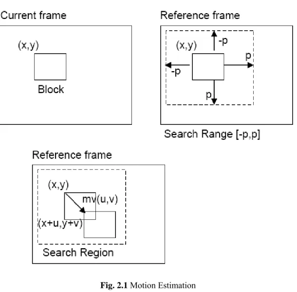
Motion estimation is the process of searching a search window in a reference frame to determine the best match for a block in a current frame based on a search criterion such as minimum Sum of Absolute Difference (SAD) [20]. The location of a block in a frame is given using the (x,y) coordinates of top-left corner of the block. The search window in the reference frame is the [-p,p] size region around the location of the current block in the current frame. The SAD value for a current block in the current frame and a candidate block in the reference frame is calculated by accumulating the absolute differences of corresponding pixels in the two blocks as shown in the following formula:
Where Bmxnis a block of size mxn,
d
=(dx, dy) is the motion vector (MV), c and r are current and reference frames respectively. Since a motion vector expresses the relative motion of the current block in the reference frame, motion vectors are specified in relative coordinates. If the location of the best matching block in the reference frame is (x+u, y+v), then the motion vector is expressed as (u,v). Motion estimation is performed on the luminance (Y) component of a YUV image and the resulting motion vectors are also used for the chrominance (U and V) components.6
Fig. 2.1 Motion Estimation
Full Search (FS) ME algorithm finds the reference block that best matches the current block by computing the SAD values for all search locations in a given search range. Although many fast search ME algorithms are developed, FS algorithm has remained a popular candidate for hardware implementation because of its regular dataflow and good compression performance [10, 21]. Since FS algorithm has a high computational complexity, FS ME hardware consume large amount of power.
7
2.2. 16 Processing Element Fixed Block Size Motion Estimation Hardware
The first ME hardware has 16 processing elements and implements fixed block size FS ME algorithm. This ME hardware is implemented by Can Hankendi and Oğuzhan Ablak [22]. In this thesis, this ME hardware implementation is verified and optimized.
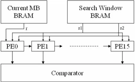
The block diagram of the ME hardware implementing FBS FS ME algorithm using 16 PEs is shown in Fig. 2.2. This ME hardware is based on the Motion Vector based Linear Arrays architecture proposed in [20]. This ME hardware finds a MV for a 16x16 Macroblock (MB) based on minimum SAD criterion in a search range of [-8,7] pixels.
Fig. 2.2 16 PE FBS ME Architecture
The pixels in the current MB are stored in a Block RAM (BRAM). The pixels in the search window are stored in a dual-port BRAM. Since PE array needs a pixel from each part of search window in one cycle, the pixels in the left half of the search window are read from s1 port and the pixels in the right half of the search window are read from s2 port. The search window and current block memory organization can be seen in Fig. 2.3.
8
Fig. 2.3 Search Window and Current Block Memory Organization
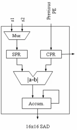
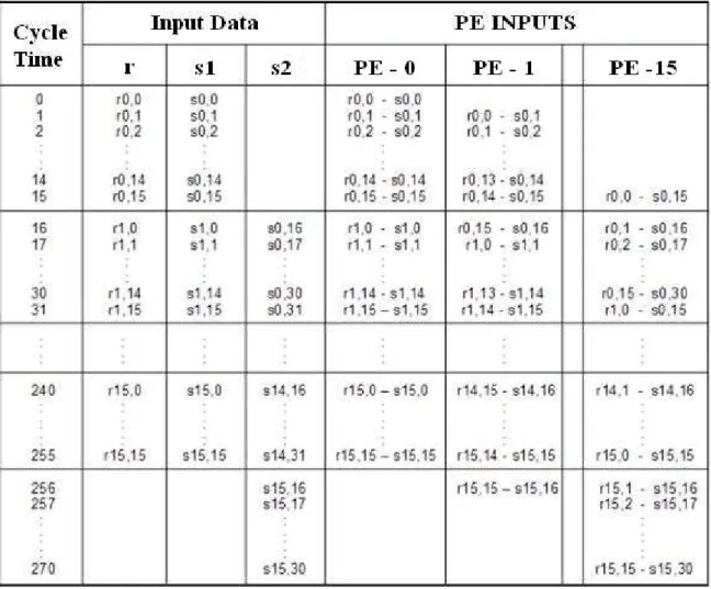
Each PE is composed of a multiplexer, current pixel register, search pixel register, a subtractor and an accumulator as shown in Fig. 2.4 Each PE calculates the SAD of a search location in 256 clock cycles. Each PE starts calculating the SAD of its search location one cycle later than the previous PE in order to reuse the current pixel. Therefore, PEs calculate the SAD values of 16 search locations in 256+15=271 clock cycles. The data flow of the PEs is shown in Table 2.1 where s(x, y) is a search window pixel and r(x, y) is a current block pixel.
9
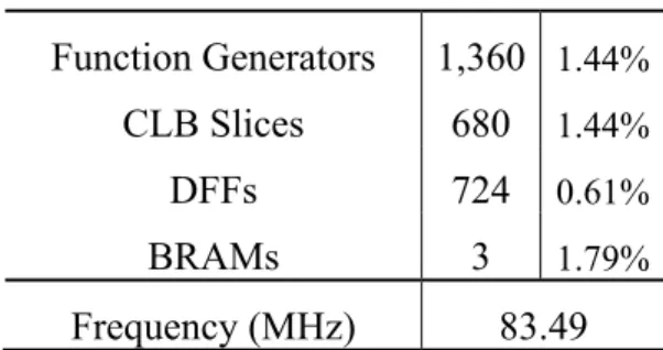
The Verilog RTL code of this ME hardware is synthesized to a 2V8000ff1157 Xilinx Virtex II FPGA with speed grade 4 using Mentor Graphics Precision RTL tool. The resulting netlist is placed and routed to the same FPGA using Xilinx ISE tool. The FPGA resource usage and the maximum clock frequency of the routed design are given in Table 2.2. The design takes 5283 clock cycles to process a MB. Therefore, it processes a CIF (352x288) frame in 25.04 ms (396 MBs * 5283 clock cycles per MB * 11.97 ns clock cycle = 25.04 ms). Therefore, it can process 1000/25.04 = 40 CIF frames per second.
10 Function Generators 1,360 1.44% CLB Slices 680 1.44% DFFs 724 0.61% BRAMs 3 1.79% Frequency (MHz) 83.49
Table 2.2 The FPGA Resource Usage and the Maximum Clock Frequency of 16PE FBS ME Hardware
2.3. 256 Processing Element Variable Block Size Motion Estimation Hardware
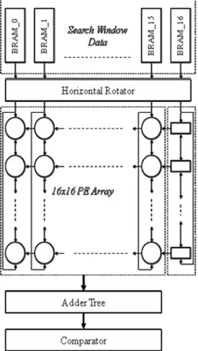
The second ME hardware has 256 processing elements and implements VBS FS ME algorithm. This ME hardware is designed and implemented by Onur Can Ulusel and Turhan Karadeniz [23]. The block diagram of the proposed ME hardware architecture for implementing VBS FS ME algorithm using 256 PEs is shown in Fig. 2.5. In the proposed architecture, a 2-D systolic PE array is used and all the PEs are capable of shifting data down, up and left. Each circle in the figure represents a PE. This ME hardware calculates a MV for a 16x16 MB in one cycle in a search range of [-16, 15] pixels.
11
Fig 2.5 Architecture of 256 PE ME Hardware
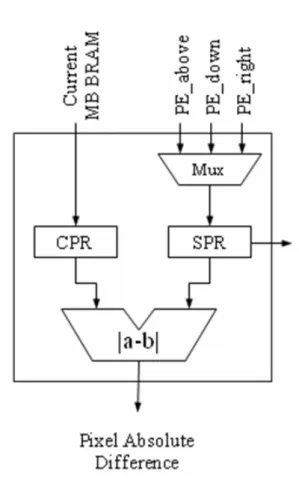
The architecture of a PE is shown in Fig. 2.6 Each PE calculates the absolute difference between a pixel in the current MB and a pixel in the search window. The SAD of a search location is calculated by adding the absolute differences calculated by PEs using an adder tree. This ME hardware is highly pipelined and its latency is eight clock cycles; one cycle for synchronous read from BRAM, one cycle for horizontal shifting, one cycle for SAD computation in 2-D systolic PE array, two cycles for the adder tree generating 4x4 SADs and three cycles for the adder tree generating 41 MVs for 7 different block sizes.
12
Fig. 2.6 PE of 256PE Hardware
The proposed 256PE VBS ME hardware searches the search locations in a search window column by column in a zigzag pattern. Most of the proposed ME hardware architectures using 256 PEs use a vertical search flow and when the end of a column is reached the search location at the top of the next column is searched as shown in Fig. 2.7.a. Therefore, it is required to either broadcast multiple pixels into the PEs [24] or delay all the PEs until they are filled. There are 256PE ME hardware architectures using a 2-D systolic PE array and searching the search window in a zigzag pattern as shown in Fig.2.7.b [25]. However, these architectures either use both row and column aligned memories or use data duplication. The proposed architecture overcomes this problem by using a pipeline of 16 8-bit temporary registers.
13
In the proposed 256PE VBS ME hardware, the search starts at top left search location of the search window and proceeds down until the last search location of this column is searched. Then, the search continuous with the last search location of the next column and proceeds up until the first search location of this column is searched. Only 16 new search window pixels are required by the PE array in each cycle to calculate the SAD of the next search location regardless of its position in the search window.
The data flow of the PEs is shown in Table 2.3 where S(x, y) is a search window pixel. Current MB pixels are not shown in the table, because each PE stores the same current MB pixel (e.g. PE(0,0) stores C(0,0)) while searching all the search locations in a search
Fig 2.7 (a) Vertical Search Flow (b) Zigzag Search Flow
1st Column 16th Column Temp Column
Clock
PE(0,15) PE(0,14) … PE(0,0) … PE(15,15) PE(15,14) … PE(15,0) Reg15 Reg14 … Reg0
0 S(0,0) nop nop R(15,0) nop nop R(16,0) nop nop
1 S(0,1) S(0,0) nop R(15,1) R(15,0) nop R(16,1) R(16,0) nop
… … … … … … … … … … 15 S(0,15) S(0,14) … S(0,0) … S(15,15) S(15,14) … S(15,0) S(16,15) S(16,14) … S(16,0) 16 S(0,16) S(0,15) S(0,1) S(15,16) S(15,15) S(15,1) S(16,16) S(16,15) S(16,1) 17 S(0,17) S(0,16) S(0,2) S(15,17) S(15,16) S(15,2) S(16,17) S(16,16) S(16,2) … … … … … … … … … … 46 S(0,46) S(0,45) … S(0,31) … S(15,46) S(15,45) … S(15,31) S(16,46) S(16,45) … S(16,31) 47 S(1,46) S(1,45) S(1,31) S(16,46) S(16,45) S(16,31) nop nop nop
48 S(1,45) S(1,44) S(1,30) S(16,45) S(16,44) S(16,30) nop nop S(17,30) … … … … … … … … … … 78 S(1,15) S(1,14) … S(1,0) … S(16,15) S(16,14) … S(16,0) S(17,15) S(17,14) … S(17,0) … …
1007 S(31,46) S(31,45) S(31,31) S(46,46) S(46,45) S(46,31) nop nop nop
1008 S(31,45) S(31,44) S(31,30) S(46,45) S(46,44) S(46,30) nop nop nop
… … … … … … … … … … 1038 S(31,15) S(31,14) … S(31,0) … S(46,15) S(46,14) … S(46,0) nop nop … nop
14
window. The PE array is filled in the first 15 cycles. While searching the search locations in the first column of the search window, in each cycle, vertical up shift is performed in the PE array and all the PEs except the ones in the last row are provided search window pixels from their neighboring PEs. PEs in the last row of PE array, in each cycle, read 16 new search window pixels from 16 BRAMs.
The 17th BRAM is used to be able to perform a left shift in the PE array after all the search locations in a column is searched. The 17th BRAM is connected to the temporary registers and by the time there is a need for left shift, the pixels needed for the right most PEs in the PE array become ready in these temporary registers. After the search locations in the first column are searched, a left shift is performed in the PE array while the PEs in the 16th column of the PE array receive search window pixels from the temporary registers.
While searching the search locations in the second column of the search window, in each cycle, vertical down shift is performed in the PE array and all the PEs except the ones in the first row are provided search window pixels from their neighboring PEs. PEs in the first row of PE array, in each cycle, read 16 new search window pixels from 16 BRAMs.
Each BRAM stores the pixels in every 17th column of the search window, e.g. the first BRAM stores the pixels in the 1st, 18th and 35th columns. The order of the search window pixels read from the BRAMs is static. However, the order of the search window pixels required by the PE array and the temporary registers varies depending on the column being processed. This problem is solved by reordering the 16+1 pixels in a search MB row by the horizontal rotator hardware.
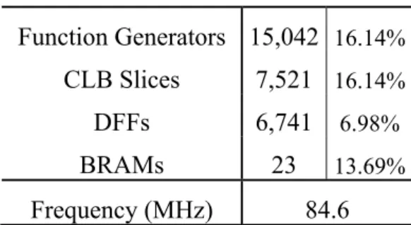
The Verilog RTL code of this ME hardware is synthesized to a 2V8000ff1157 Xilinx Virtex II FPGA with speed grade 4 using Mentor Graphics Precision RTL tool. The resulting netlist is placed and routed to the same FPGA using Xilinx ISE tool. The FPGA resource usage and the maximum clock frequency of the routed design are given in Table 2.4. The design takes 1085 clock cycles to process a MB. Therefore, it can process a VGA (640x480) frame in 15.38 ms (1200 MBs * 1085 clock cycles per MB * 11.82 ns clock cycle = 15.38 ms). Therefore, it can process 1000/15.38 = 65 VGA frames per second.
15 Function Generators 15,042 16.14% CLB Slices 7,521 16.14% DFFs 6,741 6.98% BRAMs 23 13.69% Frequency (MHz) 84.6
Table 2.4 The FPGA Resource Usage and the Maximum Clock Frequency of 256PE VBS ME Hardware.
16 CHAPTER III
DYNAMIC POWER ESTIMATION OF MOTION ESTIMATION HARDWARE
There are many papers in the literature about power estimation of ASIC hardware implementations [12-14]. However, there is not much work on power estimation of FPGA hardware implementations [3, 26]. These papers mostly address the problem of dynamic power estimation, because the amount of static power that a FPGA device consumes is measured and given by the manufacturer of that specific device.
Power estimation techniques can be classified into two categories depending on their abstraction levels [27]. High level techniques generally consume less time and require less information about the design than the low level techniques. The side effect of this is low accuracy. The high level techniques that are proposed in the literature have average errors ranging from %3 to %35.
3.1 High Level Dynamic Power Estimation
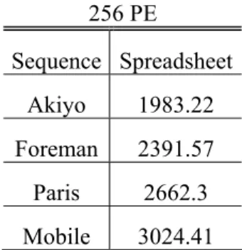
FPGA device manufacturers provide power estimation tools in different abstraction levels. For high level power estimation, Xilinx provides a spreadsheet for each device it produces [28]. These spreadsheets use some data about the design like total number of slices used, average switching activity and average fan-out of the slices. Table 3.1 shows the dynamic power estimation results obtained by Xilinx Virtex II spreadsheet for 256 PE ME hardware for four different sequences.
17 256 PE Sequence Spreadsheet Akiyo 1983.22 Foreman 2391.57 Paris 2662.3 Mobile 3024.41
Table 3.1 Xilinx Spreadsheet Dynamic Power Estimation Results for 256 PE ME Hardware (mW)
The dynamic power consumption of external busses and external RAMs can be estimated using high level power estimation techniques. A formula for calculation of the dynamic power consumption of external buses is given in [29].
where C is the average capacitance of the lines, VDD is the supply voltage and f is average switching activity frequency. For 50MHz bus speed, 1.5V supply power and an average of 15x10-12F interconnect capacitance, average power consumed for accessing 40 CIF (352x288) frames of Foreman sequence is 7.4 mW, which is quite small when compared to power consumption inside the FPGA.
There is an open source tool called CACTI for calculating external RAM power [30]. According to CACTI 5.3, for a 90nm technology 64 MB DRAM operating at 50MHz, acquiring 40 CIF (352x288) frames of Foreman sequence consumes an average of 2.36nJ energy per 8-bit read, which corresponds to 11.96 mW dynamic power.
In [2], average dynamic power consumption of different building blocks of FPGAs are gathered from the device manufacturer, and the average dynamic power of an FPGA implementation is calculated by analyzing the average switching activity of each block by software. This technique has a low accuracy. The estimations have a %18 average error and a %27 maximum error for randomly selected generic circuits.
18
In [13], a high level dynamic power estimation technique is proposed. Instead of performing an RTL level simulation, this technique extracts internal switching activity of the circuit at system level by software and then uses the extracted data on a commercial RTL level dynamic power estimation tool. Dynamic power estimations of the technique are on the average %3 different than the estimations depending on RTL level simulations and the actual estimation time is reduced to %8.3 of the original estimation time.
In [31], average dynamic power of FPGAs are calculated by grouping the inputs and outputs into related groups and calculating the effects of total switching activity of these groups with a training data set. This approach has a very high accuracy for small designs such as a single adder, but estimation accuracy for bigger and complex designs are not provided in the paper.
3.2 Low Level Dynamic Power Estimation
Low level power estimation techniques use hardware implementation details and input data, and they take longer than high level techniques. The advantage of low level techniques is their higher accuracy. FPGA device manufacturers provide low level power estimation tools. The power consumption of a hardware implementation on a Xilinx FPGA can be very accurately estimated using Xilinx XPower tool [15]. Since the switching activity is input pattern dependent, in order to estimate the dynamic power consumption, timing simulation of the placed and routed netlist of that hardware implementation is done for several input patterns using Mentor Graphics ModelSim and the signal activities are stored in a Value Change Dump (VCD) file. This VCD file is used for calculating the switching activity of the hardware implementation in the FPGA.
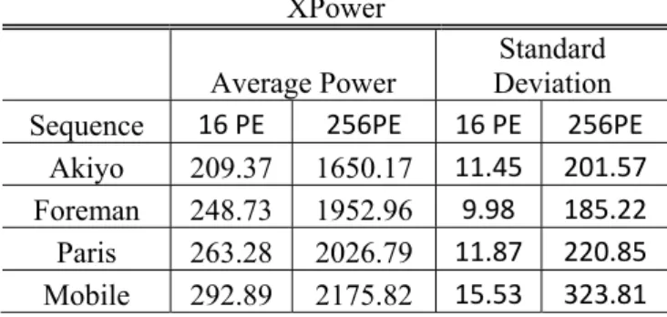
Table 3.2 shows average dynamic power estimation results obtained by XPower for both ME hardware for four different sequences. Fig. 3.1, 3.2, 3.3, and 3.4 show dynamic power estimation results obtained by XPower for 256PE ME hardware for the first frames of
19
four CIF sequences. Table 3.3 shows the difference between the high level Xilinx spreadsheet power estimations and the low level XPower power estimations.
XPower
Average Power Deviation Standard
Sequence 16 PE 256PE 16 PE 256PE
Akiyo 209.37 1650.17 11.45 201.57
Foreman 248.73 1952.96 9.98 185.22
Paris 263.28 2026.79 11.87 220.85
Mobile 292.89 2175.82 15.53 323.81
Table 3.2 XPower Average Dynamic Power Estimation Results for 16PE and 256 PE. (mW) 256 PE
Sequence XPower Spreadsheet Difference
Akiyo 1650.17 1983.22 20.16%
Foreman 1952.96 2391.57 22.42%
Paris 2026.79 2662.30 31.34%
Mobile 2175.82 3024.41 38.98%
Table 3.3 XPower and Xilinx Spreadsheet Average Dynamic Power Estimation Comparison for 256 PE. (mW)
20
Fig. 3.1 Macroblock by Macroblock Dynamic Power Estimation of 256 PE Hardware for the First Frame of Foreman Sequence (mW)
Fig. 3.2 Macroblock by Macroblock Dynamic Power Estimation of 256 PE Hardware for the First Frame of Mobile Sequence (mW)
21
Fig. 3.3 Macroblock by Macroblock Dynamic Power Estimation of 256 PE Hardware for the First Frame of Akiyo Sequence (mW)
Fig. 3.4 Macroblock by Macroblock Dynamic Power Estimation of 256 PE Hardware for the First Frame of Paris Sequence (mW)
22
Fig. 3.5 Xilinx XPower Tool
The gate-level timing simulation based power estimation using XPower is very time consuming for large designs. For 16 PE ME hardware, the power estimation of ME of a pair of CIF (352x288) frames takes an average of 6 hours in an HP workstation with two Intel 2.3 GHz 4-Core processors. For 256 PE ME hardware, the power estimation of same operation takes an average of 18 hours in the same HP workstation.
Zero delay gate-level simulation is a way of decreasing the complexity of low level dynamic power estimation. In zero delay gate-level simulation, delays of all gates are considered as zero, and therefore the glitches are ignored. The average difference between the estimation results of normal and zero delay gate-level simulations are %11 for 256 PE ME hardware and the total power estimation time is reduced by 2 hours.
In [12], a low-level probabilistic power estimation technique is proposed. This technique is applied only to the combinational parts of a circuit. It is claimed to be very accurate and it has a maximum error of %7. However, because of its high complexity it can only be used on small circuits of a few thousand gates.
23
3.3. A Novel Dynamic Power Estimation Technique for Motion Estimation Hardware
Generic power estimation techniques like [31] depend on finding a high correlation between the input switching activity and the average dynamic power. Correlation (β) is the indicator of linear dependence between two sets of variables {X1,Y1; … ; Xn,Yn}. Absolute value of correlation can be between 0 (no dependence at all) and 1 (strong linear dependence) and calculated with this formula:
where Xi is the ith measurement of X, X΄ is the mean value and sx is the standard deviation of the set {X1, …, Xn}.
For FS ME hardware designs correlation between input switch amount and dynamic power is very low (β=0.6 for 256 ME), because the input data is stored and reused in the hardware many times and in many different orders. FS ME hardware has a special property which can be exploited for more accurate high level power estimation. The PEs that are used in the FS ME hardware are identical and they are the dominant source of power consumption as seen in the Table 3.4. The Clock and Address Generation parts have same power consumption for all MBs, and the other parts have a very small effect on the overall power consumption of ME hardware. 256 PE Power (mW) Percentage Clock 291.00 16.55% Address Generation 61.08 3.47% PE SAD Calculation 1232.49 70.11% Adder Tree 97.40 5.54% BRAMs 35.19 2.00% Others 40.84 2.32% Total 1758.00 100.00%
Table 3.4 Average Dynamic Power Consumption of Different Parts of 256PE ME Hardware at 50MHz (mW)
24
The total input switching activity of PEs showed a strong correlation (β=0.92 for Foreman sequence and β=0.96 in average are calculated in MATLAB) with the overall dynamic power consumption of 256PE ME hardware. As seen in Fig. 3.6, there is a linear dependence between input switching activity of PEs and the dynamic power consumption of ME hardware. Therefore, a linear formula “Pdyn=ax+b” can be found for the FS ME hardware where (x) is the input switching activity of PEs and (a) and (b) are constants which can be found by using some training data. In this way, instead of using time consuming low level dynamic power estimation, dynamic power consumption of FS ME hardware can be estimated by software with a small error.
Fig. 3.6 Dynamic Power (mW) vs. Input Switch activity of PEs per MB for training data set. The training set for 256PE ME hardware is selected from random frames of four different video sequences (Foreman, Mobile, Akiyo, Paris). The power estimations of the frames in the training set are done with XPower. Then, a linear formula is found using the power consumption estimations and input switching activity. A large number of random frames are selected as comparison set, and the power estimations of these frames obtained by
25
the formula found above are compared with the power estimations of these frames obtained by XPower. The average estimation difference is found to be around %3 while maximum difference is %13. This is an important achievement since power estimation time is reduced significantly with a small amount of loss in accuracy. The detailed results are shown in Fig. 3.7 and Table 3.5. Average Max Akiyo 3.40% 12.75% Paris 3.19% 12.98% Mobile 2.91% 12.34% Foreman 3.44% 11.70% All 3.25% 12.98%
Table 3.5 Average and Maximum Differences Between the Proposed Technique and XPower for Power Estimation of 256PE ME Hardware
26 CHAPTER IV
DYNAMIC POWER REDUCTION OF MOTION ESTIMATION HARDWARE
4.1. Glitch Reduction and Clock Gating
Glitch reduction and clock gating are two well known techniques for power reduction in FPGAs [32]. The impact of glitch reduction and clock gating techniques on the power consumption of 16PE FBS ME hardware is quantified on a Xilinx Virtex II FPGA at 50MHz for QCIF size Foreman and Mobile video sequences.
Glitch is a spurious transition at a node within a single cycle before the node settles to the correct value [16]. Unlike ASICs, in which signals can be routed using any available silicon, FPGAs implement interconnects using fixed metal tracks and programmable switches. The relative scarcity of programmable switches often forces signals to take longer routes than would be seen in an ASIC. As a result, the potential for unequal delays among signals, hence the creation of glitches, is more likely than the case in an ASIC. Therefore, reducing glitches by pipelining is an effective power reduction technique for FPGAs.
27
Pipeline registers are added inside the PEs, as shown in Fig. 4.1, and their impact is quantified on the power consumption of 16PE FBS ME hardware for Foreman and Mobile video sequence. As it can be seen in Table 4.1, an average dynamic power reduction of 32% is achieved for PEs and an average dynamic power reduction of 20% is achieved for 16PE FBS ME hardware. Fig. 4.2 shows the improvement in each MB for a random frame of QCIF (176x144) Foreman sequence.
Fig. 4.2 Dynamic Power Consumption of 16 PE ME Hardware for a Random Frame of Foreman Sequence at 50 MHz
28
Clock signal power is a major component in the overall power consumption of FPGAs [17]. Clock gating is a well known technique for reducing dynamic power by disabling the clock for the unused parts of a circuit. This avoids unnecessary power dissipation in the clock signal and in the unused parts of a circuit [18].
Clock gating in Xilinx FPGAs can be done in two different ways. The first way is to control the individual clock enable inputs of the registers. This has a smaller impact on the dynamic power consumption of the clock lines because the clock lines that are connected to the register still consume power. A Verilog code that gates the clock input of a single register is shown below.
Fig. 4.3Clock Tree (a) Before (b) After Clock Gating. Foreman
Normal Pipelined Clock Gating
Clock 45.57 49.53 49.56
PE 165.18 107.46 106.34
Others 37.98 37.75 36.49
Total 248.73 194.74 192.39 Mobile
Normal Pipelined Clock Gating
Clock 45.57 49.53 49.56
PE 199.00 138.85 136.47
Others 48.32 50.25 48.24
Total 292.89 238.63 234.27 Table 4.1 Average Dynamic Power (mW) of
29 always @(posedge clk)
if (enable) a <=b;
The second way to implement clock gating in Xilinx FPGAs is to use different clock trees for different parts of the circuit and control the trees from the tri-state buffers at their source. In this way, when the clock tree is gated, there is no switching activity in the clock lines and, therefore, more dynamic power is saved. The side effect of this is the increased total dynamic power consumption of the clock trees when they are active.
Xilinx Virtex-II FPGA has the ability to route eight clock trees [33]. After applying the glitch reduction technique, we redesigned our 16PE FBS ME hardware with two clock trees as shown in Fig. 4.3. The first clock tree is connected to the PEs and part of the control unit. This clock tree is gated when these parts are inactive. The second clock tree is connected to the rest of the ME hardware. This clock tree is not gated. Additional clock tree comes with a small power overhead because of the clock management circuit and the clock tree capacitance. However, the power reduction achieved by clock gating is larger than this overhead. As it can be seen in Table 4.1, average dynamic power reduction of 2% is achieved by clock gating after glitch reduction.
4.2 A Novel Power Reduction Technique for Motion Estimation Hardware
In this thesis, a new power reduction technique for ME hardware is proposed. This technique is applied to both 16PE FBS ME hardware and 256PE VBS ME hardware, and compared with existing least significant bit pixel truncation technique in terms of power consumption and PSNR. A pseudo-code of the proposed technique is shown below.
// x is the number of MSBs compared // y is the minimum hamming distance temp = pixel[0];
for (i =1; i<number of pixels; i=i+1) begin
30 hd = hammingdistance(pixel[i], temp);
if (pixel[i][8,...,8-(x-1)] == temp[8,...,8-(x-1)] && hd>y) pixel[i]=temp;
else
temp=pixel[i]; end
The proposed technique reduces the switching activity in a ME hardware by assigning the value of the previous pixel to the current pixel if the current pixel is arithmetically close to the previous pixel and there is a large hamming distance between the two pixels. The parameters used for making this decision are important for the resulting video quality and the amount of power reduction.
The first parameter for determining whether the current pixel will be changed is the maximum arithmetic distance allowed between the two pixels. If the arithmetic distance is smaller than a threshold, then the current pixel is changed. In our hardware implementation, we determine whether the arithmetic distance is smaller than a threshold by comparing most significant x bits of the two pixels, instead of subtracting consequent pixels. The experimental results showed that x=3 provides significant power reduction with a small PSNR loss.
The second parameter for determining whether the current pixel will be changed is the minimum hamming distance (y) allowed between the two pixels. A large hamming distance means that there are many switching bits between the two pixels so it is preferable to change the current pixel value. A small hamming distance indicates that changing the current pixel value may not decrease the power consumption enough to balance the PSNR loss.
In order to calculate the hamming distance of two numbers, first, two numbers are XORed, and then the number of 1’s in the XORed result is found. Since BRAMs consume small amount of power, we used them as look-up tables for finding the number of 1’s in the XORed result. The BRAM is initialized with the data needed, the XORed result is used as the address to this BRAM and the BRAM returns the hamming distance value.
31
Fig. 4.4 Modified 256 PE ME Hardware
We added a pixel modification hardware implementing the proposed technique into both ME hardware. The 256PE VBS ME hardware with the proposed technique is shown in Fig. 4.4. Each search BRAM input enters into its own decision module and each decision module determines whether the current pixel will be changed by finding the hamming distance and the arithmetic distance between the current pixel and previous pixel. The hamming distance finder in each decision module is implemented as a lookup table in a BRAM. The arithmetic distance finder is a simple comparator which compares the most significant x bits of current pixel and previous pixel.
32
The impact of the proposed technique on the power consumption and PSNR of 16PE FBS ME hardware and 256PE VBS ME hardware is quantified on a Xilinx Virtex II FPGA at 50MHz for QCIF and CIF size Foreman and Mobile video sequences respectively. The power consumption results of the ME hardware are estimated using Xilinx XPower tool. PSNR results of the proposed technique are obtained by reconstructing the current frame from the search frame and calculating the PSNR between the current frame and the reconstructed current frame using software models of the 16PE FBS ME hardware and 256PE VBS ME hardware including the proposed technique.
Foreman
PSNR(dB) diff Power(mW) diff
Normal 33.40 0.00 194.85 0.00% x=3, y=2 33.37 -0.03 175.03 10.17% x=3, y=1 32.96 -0.44 147.86 24.12% trunc1 33.40 0.00 179.80 7.72% trunc2 33.05 -0.35 157.90 18.96% Mobile
PSNR(dB) diff Power(mW) diff
Normal 25.94 0.00 228.54 0.00%
x=3, y=2 25.93 -0.01 209.14 8.49%
x=3, y=1 25.90 -0.04 184.37 19.33%
trunc1 25.92 -0.02 213.30 6.67% trunc2 25.83 -0.11 190.94 16.45% Table 4.2 Average Dynamic Power and PSNR of 16PE FBS ME
33
The power consumption of the 16PE FBS ME hardware and 256PE VBS ME hardware for the x and y parameter values providing significant power reduction with a small PSNR loss are shown in Tables 4.2 and 4.3 respectively. The results indicate that proposed technique for x=3 and y=2 achieves more power reduction than one bit truncation (trunc1) with a similar PSNR loss and proposed technique for x=3 and y=1 achieves more power reduction than two bit truncation (trunc2) with a similar PSNR loss.
The area and performance of 16PE FBS ME hardware and 256PE VBS ME hardware without and with the proposed technique are shown in Table 4.4.
16PE FBS ME 256PE VBS ME Normal Proposed Technique Normal Proposed Technique Function Generators 1,360 1,396 15,042 15,984 CLB Slices 680 698 7,521 7,992 DFFs 724 796 6,741 7,648 BRAMs 3 4 23 38 Frequency (MHz) 83.49 83.53 84.60 75.90
Table 4.4 Area and Performance of 16PE FBS ME Hardware and 256PE VBS ME Hardware
Foreman
PSNR(dB) diff Power(mW) diff
Normal 33.56 0.00 1862.70 0.00% x=3, y=2 33.46 -0.10 1620.96 12.98% x=3, y=1 32.31 -1.25 1365.57 26.69% trunc1 33.56 0.00 1769.47 5.01% trunc2 32.63 -0.93 1496.63 19.65% Mobile
PSNR(dB) diff Power(mW) diff
Normal 23.12 0.00 2283.13 0.00%
x=3, y=2 23.12 0.00 1954.64 14.39%
x=3, y=1 23.12 0.00 1797.74 21.26%
trunc1 23.13 0.01 2086.63 8.61% trunc2 23.14 0.02 1826.91 19.98% Table 4.3 Average Dynamic Power and PSNR of 256PE VBS ME
34
4.3 Developing New Dynamic Power Reduction Techniques Using Proposed Dynamic Power Estimation Technique
Developing new power reduction techniques requires fast and accurate power estimation techniques for quantifying the impact of the proposed power reduction technique. To assess the effectiveness of our proposed dynamic power estimation technique for developing new dynamic power reduction techniques, dynamic power estimations of the 256PE ME hardware are done after the application of two dynamic power reduction techniques.
First, the proposed power estimation technique is used after the LSB truncation technique. Fig. 4.5 shows the data points obtained by gate-level simulation based power estimation of 256 PE ME hardware using XPower and the P = ax + b line found in MATLAB by curve fitting.
35
Fig. 4.5 Dynamic Power (mW) vs. Input Switch Activity of PEs per MB for Training Data Set for LSB Truncation Technique
Then, four frames are randomly selected from two different sequences for the comparison set. Data points obtained by gate-level simulation based power estimation of these frames and the P = ax + b line that is derived from the training set is shown in Fig. 4.6. As seen in Table 4.5, the proposed power estimation technique achieved good results for the frames in comparison set. For one bit truncation (Trunc1), it has an average difference of %3.45 from the XPower results while the maximum difference is %13.5. However, it performed worse for two bit truncation (Trunc2), where the average difference is %4.4 while the maximum difference is around %25.
36
Average Difference Max. Difference
Foreman Mobile Foreman Mobile
Trunc1 3.87% 2.99% 13.52% 9.92%
Trunc2 5.26% 3.62% 25.65% 20.60%
Table 4.5 Average and Maximum Differences of the Proposed Technique for Four Frames in Two Different Video Sequences
Fig. 4.6 Dynamic Power (mW) vs. Input Switch Activity of PEs per MB for Comparison Data Set for LSB Truncation Technique.
Next, the proposed power estimation technique is used after the proposed Hamm-Arith technique. Gate-level simulation based power estimations of the modified 256 PE ME hardware using the frames in the training set are done and a P = ax + b formula is obtained. The data points and ax + b line is shown in Fig. 4.7.
37
Fig. 4.7 Dynamic Power (mW) vs. Input Switch Activity of PEs per MB for Training Data Set for Hamm-Arith Technique
Again, four frames are randomly selected for comparison set. Data points obtained by gate-level simulation based power estimation of these frames and the P = ax + b line that is derived from the training set is shown in Fig. 4.8. As seen in Table 4.6., the proposed power estimation technique performs quite well for (x=3, y=2) where the average difference is %4.25 and the maximum difference is around %28 for a few data points. However, for (x=3, y=1), the average difference increases to %7.3 and the maximum difference is around %36.
Average Difference Max. Difference
Foreman Mobile Foreman Mobile
x=3, y=2 3.21% 5.30% 19.99% 27.45%
x=3, y=1 7.51% 7.11% 36.43% 29.28%
Table 4.6 Average and Maximum Differences of the Proposed Technique for Four Frames in Two Different Video Sequences
38
Fig. 4.8 Dynamic Power (mW) vs. Input Switch Activity of PEs per MB for Comparison Data Set for Hamm-Arith Technique
The results show that if a power reduction technique only changes the input data order of the ME hardware, the proposed dynamic power estimation technique can be used to quickly estimate the effectiveness of that technique. However, if the architecture of the ME hardware is modified, the accuracy of the power consumption estimations decrease. Therefore the proposed power estimation technique should be improved for this case.
39 CHAPTER V
CONCLUSIONS AND FUTURE WORK
In this thesis, we proposed a novel dynamic power estimation technique for full search ME hardware. We estimated the power consumption of two full search ME hardware implementations on a Xilinx Virtex II FPGA using several existing high and low level dynamic power estimation techniques and our technique. Gate-level timing simulation based power estimation of full search ME hardware for an average frame using Xilinx XPower tool takes 6 - 18 hours in a state-of-the-art PC, whereas estimating the power consumption of the same ME hardware for the same frame takes a few seconds using our technique. The average and maximum difference between the power consumptions estimated by our technique and the power consumptions estimated by XPower tool for four different video sequences are %3 and %13 respectively.
We also proposed a novel dynamic power reduction technique for ME hardware. We quantified the impact of glitch reduction, clock gating and the proposed technique on the power consumption of two full search ME hardware implementations on a Xilinx Virtex II FPGA using Xilinx XPower tool. Glitch reduction and clock gating together achieved an average of 21% dynamic power reduction. The proposed technique achieved an average of 23% dynamic power reduction with an average of 0.4dB PSNR loss. The proposed technique achieves better power reduction than pixel truncation technique with a similar PSNR loss.
We also showed that our dynamic power estimation technique can be used for developing novel dynamic power reduction techniques. To do this, we used our technique to estimate the dynamic power consumption of the ME hardware when two different dynamic power reduction techniques are used. The results show that if a power reduction technique only changes the input data order of the ME hardware, the proposed dynamic power estimation technique can be used to quickly estimate the effectiveness of that technique. However, if the architecture of the ME hardware is modified, the accuracy of the power consumption estimations decrease. Therefore the proposed power estimation technique should be improved for this case.
40
As a future work, the proposed dynamic power estimation technique can be improved by taking other parts of the ME hardware design into consideration. It can be improved to make peak dynamic power consumption estimations in addition to average dynamic power consumption estimations. The proposed dynamic power reduction technique can be improved by further reducing the overhead of the pixel modification block. The effectiveness of the proposed power estimation and reduction techniques can be evaluated on larger frame sizes such as VGA (640x480) or 1080p HD (1920x1080). The proposed power estimation and reduction techniques can be applied to other ME algorithms such as diamond search, hexagon based search and hierarchical search. They can also be applied to ASIC implementations of these ME hardware designs.
41
REFERENCES
[1] The International Technology Roadmap for Semiconductors. (2005 Edition) [Online]. http://www.itrs.net/Links/2005ITRS/Home2005.htm
[2] Degalahal V. and Tuan T., "Methodology for High Level Estimation of FPGA Power Consumption", Asia and South Pacific Design Automation Conference, Vol. 1, pp. 657-660, Jan 2005.
[3] Abdelli N., Fouilliart A.-M., Mien N., Senn E., "High-Level Power Estimation of FPGA", IEEE International Symposium on Industrial Electronics, pp. 925-930, June 2007.
[4] Muhammad Shafique, Lars Bauer, and Jörg Henkel, "3-Tier Dynamically Adaptive Power-Aware Motion Estimator for H.264/AVC Video Encoding", International Symposium on Low Power Electronics and Design, pp. 147-152, 2008.
[5] B.-S. Kim and J.-D. Chung, "VLSI Architecture for Low Power Motion Estimation Using High Data Access Reuse", The First IEEE Asia Pacific Conference on ASICS, pp. 162-165, Aug 1999.
[6] S.-H. Han, S.-W. Kwon, T.-Y. Lee, M.-K. Lee, "Low Power Motion Estimation Algorithm Based on Temporal Correlation and its Architecture", Sixth International, Symposium on Signal Processing and its Applications, Vol. 2, pp. 647-650, Aug 2001. [7] Z.-L. He, C.-Y. Tsui, K.-K. Chan, and M. L. Liou, “Low-power VLSI Design for Motion
Estimation Using Adaptive Pixel Truncation,” IEEE Transactions on Circuits and Systems for Video Technology, vol. 10, no. 5, pp. 669–678, Aug 2000.
[8] C.-Y. Chen, S.-Y. Chien, Y.-W. Huang, T.-C. Chen, T.-C. Wang, and L.-G. Chen, “Analysis and Architecture Design of Variable Block Size Motion Estimation for H.264/AVC,” IEEE Transactions on Circuits and Systems I, vol. 53, no. 3, March 2006. [9] Asral Bahari, Tughrul Arslan and Ahmet T. Erdogan, “Low Power Variable Block Size
Motion Estimation Using Pixel Truncation,” IEEE International Symposium on Circuits and Systems, pp. 3663-3666, May 2007.
[10] G. Stewart, D. Renshaw, and M. Riley, “A Novel Motion Estimation Power Reduction Technique,” International Conference on Field Programmable Logic, pp. 546–549, August 2007.
42
[11] Park, S.R. and Burleson, W., "Reconfiguration for Power Saving in Real-Time Motion Estimation", IEEE International Conference on Acoustics, Speech and Signal
Processing, Vol. 5, pp. 3037-3040, May 1998.
[12] S. T. Oskuii, P. G. Kjeldsberg; E. J. Aas, "Probabilistic Gate-level Power Estimation using a Novel Waveform Set Method", 17th ACM Great Lakes symposium on VLSI, pp. 37-42, 2007.
[13] S. Ahuja, D.A. Mathaikutty, G. Singh, J. Stetzer, S.K. Shukla, A. Dingankar, "Power Estimation Methodology for a High-Level Synthesis Framework", International Society for Quality Electronic Design, pp. 541-546, March 2009.
[14] Najm, F.N.,"Power Estimation Techniques for Integrated Circuits", 1995 IEEE/ACM International Conference on Computer-Aided Design Digest of Technical Papers, pp. 492-499, Nov. 1995.
[15] Xilinx XPower Overview [Online].
http://www.xilinx.com/products/design_resources/power_central/index.htm [16] S. J. E. Wilton, S–S. Ang and W. Luk, “The Impact of Pipelining on Energy per
Operation in Field-Programmable Gate Arrays,” International Conference on Field Programmable Logic, pp. 719-728, Aug 2004.
[17] Ian Brynjolfson and Zeljko Zilic, “Dynamic Clock Management for Low Power Applications in FPGAs,” IEEE Custom Integrated Circuits Conference, May 2000. [18] Xiaotao Chang, Mingming Zhang, Ge Zhang, Zhimin Zhang and Jun Wang, “Adaptive
Clock Gating Technique for Low Power IP Core in SoC Design,” IEEE International Symposium on Circuits and Systems, May 2007.
[19] Caglar Kalaycioglu, Onur Can Ulusel, Ilker Hamzaoglu, “Low Power Techniques for Motion Estimation Hardware”, International Conference on Field Programmable Logic, Sep 2009.
[20] V. Bhaskaran and K. Konstantinides, Image and Video Compression Standards: Algorithms and Architectures, Kluwer Academic Publishers, 2nd Edition, 1997.
[21] S. Yalcin, H. F. Ates and I. Hamzaoglu, “A High Performance Hardware Architecture for an SAD Reuse based Hierarchical Motion Estimation Algorithm for H.264 Video
Coding”, International Conference on Field Programmable Logic, August 2005. [22] Can Hankendi and Oğuzhan Ablak, “Low Power H.264 Video Encoder Design”, BS
43
[23] Onur Can Ulusel and Turhan Karadeniz, “S-Shaped Full Search Motion Estimation with Variable Block Size,SAD Reuse & Bit Truncation”, BS Graduation Project Final Report, Sabancı University, June 2008.
[24] Y. W. Huang, T. C. Wang, B. Y. Hsieh, and L. G. Chen, “Hardware Architecture Design for Variable Block-Size Motion Estimation in MPEG-4 AVC/JVT/ITU-T H.264”, IEEE International Symposium on Circuits and Systems, pp. 796–799, 2003.
[25] M. Kim, I. Hwang, and S.-I. Chae, “A Fast VLSI Architecture for Full-Search Variable Block Size Motion Estimation in MPEG-4 AVC/H.264,” Asia and South Pacific Design Automation Conference, pp. 631–634, Jan 2005.
[26] J. Becker, M. Huebner, M. Ullmann, "Power Estimation and Power Measurement of Xilinx Virtex FPGAs: Trade-offs and Limitations", 16th Symposium on Integrated Circuits and Systems Design, pp. 283-288, Sep. 2003.
[27] F. N. Najm, "A Survey of Power Estimation Techniques in VLSI Circuits", IEEE Transactions on Very Large Scale Integration Systems, pp.446-455, 1994.
[28] Xilinx Virtex II Power Estimation Spreadsheet [Online]. http://www.xilinx.com/cgi-bin/power_tool/power_Virtex2
[29] Asral Bahari, Tuğrul Arslan and Ahmet T. Erdoğan, "Interframe Bus Encoding
Technique for Low Power Video Compression", 20th International Conference on VLSI Design, pp. 691 - 698, 2007.
[30] CACTI 5.2 Website [Online]. http://quid.hpl.hp.com:9081/cacti
[31] S. Li, N.K. Jha, "High-Level Power Modeling of CPLDs and FPGAs", International Conference on Computer Design, pp. 46-51, Sep. 2001.
[32] Merve Peyiç, “Low Power IEEE 802.11n LDPC Decoder Hardware Design”, M.S. Thesis, Sabanci University, Aug 2008.
[33] Xilinx Inc., Virtex-II Platform FPGAs Complete Data Sheet, Version 3.5, 2007 [34] Esam A. Al Qaralleh and Tian-Sheuan Chang, "Fast Variable Block Size Motion
Estimation by Adaptive Early Termination", IEEE Transactions on Circuits and Systems for Video Technology, Vol. 16, No. 8, pp.1021-1026, Aug 2006.
[35] Moshnyaga V.G., "A MSB Truncation Scheme for Low-Power Video Processors", IEEE International Symposium on Circuits and Systems, Vol. 4, pp. 291-294, June 1999.