LP-NUCA: Networks-in-Cache for
High-Performance Low-Power Embedded Processors
Darío Suárez Gracia
, Student Member, IEEE
, Giorgos Dimitrakopoulos
, Member, IEEE
, Teresa Monreal Arnal,
Manolis G. H. Katevenis, and Víctor Viñals Yúfera
, Member, IEEE
Abstract—High-end embedded processors demand complex on-chip cache hierarchies satisfying several contradicting design requirements such as high-performance operation and low energy consumption. This paper introduces light-power (LP) nonuniform cache architecture (NUCA), a tiled-cache addressing both goals. LP-NUCA places a group of small and low-latency tiles between the L1 and the last level cache (LLC) that adapt better to the application working sets and keep most recently evicted blocks close to L1. LP-NUCA is built around three specialized “net-works-in-cache,” each aimed at a separate cache operation. To prove the design feasibility, we have fully implemented LP-NUCA in a 90-nm technology. From the VLSI implementation, we observe that the proposed networks-in-cache incur minimal area, latency, and power overhead. To further reduce the energy consumption, LP-NUCA employs two network-wide techniques (miss wave stopping and sectoring) that together reduce the dynamic cache energy by 35% without degrading performance. Our evaluations also show that LP-NUCA improves performance with respect to cache hierarchies similar to those found in high-end embedded processors. Similar results have been obtained after scaling to a 32-nm technology.
Index Terms—Cache organization, interconnection networks, low-power design, network-on-chip, nonuniform cache architec-ture (NUCA), VLSI.
I. INTRODUCTION
T
HE complexity and variety of embedded applications are constantly increasing, thus demanding systems with high computing capacities and low power consumption. In order to Manuscript received November 22, 2010; revised March 14, 2011; accepted May 05, 2011. Date of publication July 07, 2011; date of current version June 14, 2012. This work was supported in part by the HiPEAC European Network of Excellence through a collaboration grant and postdoctoral fellowship, by the Spanish Government and European ERDF under Grant TIN2007-66423 and Grant TIN2010-21291, the Aragón Government and European ESF through the gaZ: T48 Research Group, the Spanish Government under Consolider CSD2007-00050, and HiPEAC-2 NoE under Grant European FP7/ICT 217068. D. S. Gracia and V. V. Yúfera are with the Computer Architecture Group (gaZ), Departamento de Informática e Ingeniería de Sistemas, Instituto de Inves-tigación en Ingeniería de Aragón, Universidad de Zaragoza, E-50018 Zaragoza, Spain (e-mail: [email protected]; [email protected]).G. Dimitrakopoulos is with the Informatics and Communications Engi-neering Department, University of West Macedonia, GR-50100 Kozani, Greece (e-mail: [email protected]).
T. M. Arnal is with the Department of Computer Architecture, Universitat Politécnica de Catalunya (UPC), E-08034 Catalunya, Spain, and also with the Computer Architecture Group (gaZ), Universidad de Zaragoza, E-50018 Zaragoza, Spain (e-mail: [email protected]).
M. G. H. Katevenis is with the Foundation for Research and Tech-nology—Hellas, Institute of Computer Science (FORTH-ICS)—Computer Architecture and VLSI Systems (CARV) Laboratory, GR-70013 Heraklion, Crete, and also with the Department of Computer Science, University of Crete,GR-71409 Heraklion, Greece (e-mail: [email protected]).
Color versions of one or more of the figures in this paper are available online at http://ieeexplore.ieee.org.
Digital Object Identifier 10.1109/TVLSI.2011.2158249
TABLE I
REPRESENTATIVEPROCESSORSAMPLES OFCURRENTHIGH-ENDSOCS
(40–45 nm). SHADEDCELLSSHOW THELASTLEVELCACHE(LLC)
execute these applications and reduce costs embedded systems are integrated into system-on-chips (SoCs). Many manu-facturers offer SoCs meeting these stringent requirements. To reach the performance goal, SoCs rely on concepts and techniques previously proposed for the high-performance com-puting segment, but tuned for minimizing energy consumption. A review of current advanced embedded SoCs (40–45 nm) clearly shows how their CPUs follow close behind their high-performance siblings. Among other advanced features (see Table I), embedded processors profit from out-of-order wide issue or multithreaded execution [1]–[6].
These techniques such as wide issue and multithreading put pressure on the cache hierarchy, so its design also inherits con-cepts and techniques from the high-performance segment. For example, we can see multiported L1 data caches optimized for speed [5] and relatively big LLCs optimized for size.
An appealing proposal that has received much attention for improving the performance of the cache hierarchy has been the nonuniform cache architecture (NUCA) [7]–[21]. NUCA tackles the wire delay problem in LLCs1 by merging the L2 and the L3 into a mesh of cache banks and enabling inter-bank block migration. Hence, blocks located in the banks close to the cache controller have a lower latency that those located further apart [7].
Nevertheless, there are almost no examples of NUCA caches in high-performance embedded SoCs. A close approach is the L3 cache of NetLogic XLP832 [5]. This LLC is divided into eight independent banks, and each bank is attached to a bidirectional ring that also communicates with four DDR ports and eight private L2 caches. Since L3 cache lines are statically mapped into banks, the NetLogic solution resembles the static NUCA proposal, but with a topological change: from the original mesh to a ring.
1Driving a signal from the cache controller to the banks takes more time than the bank access itself.
To the best of our knowledge, there is little published work attempting to bring NUCA caches into SoCs. Fogliaet al.took a first step in that direction proposing a low-power NUCA for embedded LLC (triangular NUCA) [11], and Chouet al. con-tinued it with a ring for sharing L1 caches in 3-D multicore chips [20]. Following this path, in this paper, we extend light NUCAs (L-NUCAs) for deployment in embedded environments.
L-NUCA is a proposal for closing the latency gap between speed-optimized L1 caches and capacity-optimized LLC [18]. It tries to smooth this gap by retaining L1 most recently evicted blocks in a fabric of very small tiles (capacity: 8–32 KB, latency: one processor cycle). Tiles behave as a very large distributed victim cache [22] leveraging short-term temporal locality. The key novel feature of L-NUCAs is their three specialized net-works-in-cache, exploiting the availability of on-chip wires to minimize the network overhead in terms of delay, area, and power. The resulting cache offers a reduced average memory access time and a lower energy consumption regardless the or-ganization of the LLC.
To prove the scalability and benefits of L-NUCA and its networks-in-cache, we have implemented L-NUCA in a 90-nm ASIC technology. From the implementation, we draw several conclusions. First, only two types of tiles are required to build L-NUCAs of any size. Second, all of the networks-in-cache proposed in L-NUCA involve minimum overhead, and all tile operations, including cache access plus routing, fit in a single core clock cycle.2Third, on-chip wire availability can be used to reduce router complexity and, hence, latency. Fourth, cache accesses (SRAM cells and cache control logic) account for most of the total tile power, which is around 75%. Since energy consumption is crucial in embedded processors, we propose two network enhancements for its reduction based on the previous fact. We have observed that there is time to propagate a few global signals among tiles to reduce the cache accesses, Miss Wave Stopping. With subsequent simulations, we have also observed that block placement can be restricted, Sectoring, without degrading performance. Both techniques taken together form light-power NUCA (LP-NUCA), which is a specialization of L-NUCA for high-performance embedded processors.
In order to evaluate the performance and energy attained, we have fed a detailed cycle-by-cycle simulator with the energy costs from the different layout variants, finding that LP-NUCA reduces the dynamic power consumption of L-NUCAs by 35% without performance losses when running typical embedded workloads. Compared with a slightly larger conventional L2 cache that mimics the memory hierarchy of a representative high-end embedded processor, both L-NUCA and LP-NUCA, besides power savings, enable also faster execution. Similar conclusions have been derived after testing the energy behavior of LP-NUCA at 32 nm using Cacti simulations.
The remainder of this paper is organized as follows. Section II comments on the related work. Section III describes the organ-ization of the L-NUCA, while Section IV focuses on its VLSI implementation. The performance of L-NUCA is evaluated and compared to previous state-of-the-art second-level cache orga-nizations in Section V. The low-power enhancements of the 2Tile latency is mainly dominated by the cache access, which, in turn, is due to its SRAM macros.
basic L-NUCA are described in Section VI along with the en-ergy savings achieved. Finally, Section VII sketches coherence and real-time support in LP-NUCA, and Section VIII concludes the paper.
II. BACKGROUND ANDRELATEDWORK
Kim et al. introduced the NUCA organization [7]. Their focus was to reduce the impact of wire delay in LLCs, so they replace the global wires between the banks and the cache controller with a conventional 2-D mesh and wormhole routers forming the static NUCA (S-NUCA). They extend the network with the ability of inter-bank block migration, dynamic NUCA (D-NUCA), and implement them in the TRIPS processor [23].
Later, many authors have focused on improving NUCA caches, mostly in two aspects: networks and content man-agement in chip-multiprocessors. In both cases the target was LLCs. On the former group (NUCA networks), Jin et al. proposed a novel router for efficient multicast, a replacement algorithm, and a heterogeneous halo topology [8]. Murali-manohar and Balasubramonian introduced heterogeneity in the wires and in the topology with a mixed point-to-point bus network [9]. The same authors with Jouppi extended the Cacti tool to support NUCA caches and add multiple kinds of wires such as low-swing buses [10]. Fogliaet al.proposed triangular D-NUCA (TD-NUCA) for reducing power in large caches of embedded processors [11]. Chouet al.have proposed a single-cycle ring interconnection for multicore L1-NUCA on 3-D chips [20]. They connect all of the L1 caches with two counter-rotating rings and a global arbiter for granting permissions.
On the latter group (content management), Beckmann and Wood showed the complexity of block migration with requests coming from multiple processors [12]. With a similar layout, Liraet al. improve the bank replacement policy of D-NUCA based on the type of data [19]. Merinoet al.dynamically parti-tion NUCA banks to reduce access latency and improve core isolation [17]. Recently, other proposals have departed from S-NUCA to extend them with OS directed placement in order to get the advantages of D-NUCA without the migration com-plexity [13]–[16].
Most of the previous proposals target multimegabyte LLCs, and are made of large cache banks connected with conventional routers. Table II shows the routing delay, the bank latency and size, and the total NUCA size of several state-of-the-art proposals. In NUCA’s seminal work [7], small bank sizes were employed in order to keep routing delay along a bank just within a clock cycle. Subsequent designs increased the bank size and thus the corresponding routing delay for improving perfor-mance in this large LLCs environment [9], [10], [13]–[17], [19], [21], [24]. L-NUCA places a small yet fast distributed victim cache between L1 and LLCs to exploit temporal locality. Its aim is to close the latency gap between speed-optimized L1 cache and capacity-optimized LLCs, offering at the same time low-latency access to recently used blocks, virtually behaving as an L1 capacity extension mechanism. Hence, the L-NUCA
TABLE II
ROUTINGDELAY, BANKLATENCY ANDSIZE,ANDTOTALSIZE OFSEVERAL
NUCAPROPOSALS. L-NUCADOESNOTTARGETLLCAND ISPLACED
BETWEENL1AND ALARGELLC
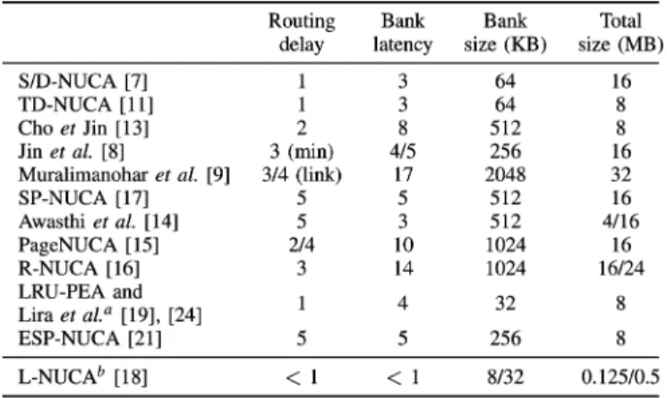
Fig. 1. Four-level L-NUCA. The numbers inside tiles represent the tile hit la-tency seen by the processor assuming single-cycle tiles.
cache works equally well whether the LLC is a conventional or a NUCA cache [18].
Most previous NUCA designs rely on conventional routers to convey messages. On the contrary, L-NUCA exploits the fact that traffic patterns within caches are quite regular by using three specialized networks-in-cache that simultaneously reduce con-trol overhead and energy consumption through the minimization of the network activities.
III. L-NUCA ORGANIZATION
Here, we first provide an overview of L-NUCA, including router organization and message types, and then it details the networks-in-cache.
A. Basic Microarchitecture
L-NUCAs extend the conventional first-level cache capacity by surrounding it with one or more levels of small cache tiles interconnected by specialized networks, as shown in Fig. 1. The cache size of a tile is chosen so that the L-NUCA cycle time (cache access plus one hop routing) is the same as the processor cycle. Since the L1 cache SRAM macros often dominate the critical path of high-end processors [25], we can make two key observations: First, caches inside the L-NUCA tiles will have lower size, or lower associativity, or lower number of ports, or a combination of all previous conditions than their corresponding
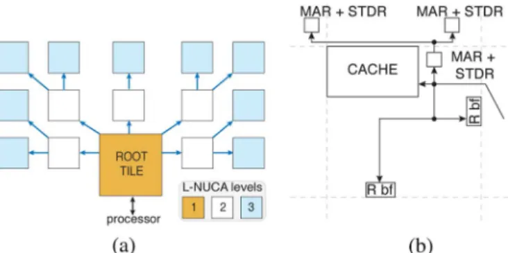
Fig. 2. L-NUCA tile main components.
L1.3Second, L-NUCA network delay will be constrained to the remainder of the cycle after the cache access completes.
In order to interface with the L-NUCA fabric, the first-level cache is slightly modified to become the so called root tile (r-tile). The rest of tiles behave as a large distributed victim cache filled with the r-tile evictions [22]. Tiles are in exclusion among them, and do not impose any mapping constraints to blocks.
Fig. 2 shows the tile internals. Apart from the cache, we dis-tinguish the three routers interfacing with the specialized net-works-in-cache, one for each cache operation:Search, Trans-port, andReplacement. All of their mechanisms are indepen-dent of the caches they connect, and the only requirement is that caches have to support load hits under previous noncompleted store hits as conventional caches do.
A load missing in the r-tile starts a miss wave that propagates across theSearch network. When a tile experiences a hit (ei-ther from the cache or from an in-transit Replacement block), the requested block is directly sent through theTransport net-workback to the r-tile that at the same time can be conveying hits from other tiles. Assuming single-cycle tiles, the numbers inside tiles of Fig. 1 represent the latency seen by the processor if that tile hits. For instance, if tile caches were direct-mapped, a block could be stored in a way at a round-trip latency of one cycle (r-tile), in three ways at three-cycle latency (tiles labeled “3”), in two more at four-cycle latency (tiles labeled “4”), etc. Eventually, when the miss wave reaches the last level, if all of the tiles have missed, aglobal missarises, and the next memory level is requested. The block coming from the next level is di-rectly written into the r-tile.
TheReplacement networkhandles the eviction traffic. When a tile receives a victim block, it first evicts another block to an ad-jacent tile so that the Search-Transport round-trip latency of the block is increased by one cycle.4Then, it writes the victim that has been waiting in the buffers of thereplacement router. For instance, both tiles labeled “4” evict the victim block through 3Also, tile cache control is simpler because tiles only provide whole blocks and not precise words as L1 caches.
TABLE III
NETWORKMESSAGES. LASTCOLUMNREPRESENTS THELINKWIDTH OFEACH
NETWORK AND ISCOMPUTEDASSUMING32-B BLOCKS, 43-BITADDRESSES,
ANDUP TO16-ENTRIESMISSSTATUSHOLDINGREGISTERS IN THEr-TILE. EXTRATHREEBITS AREINCLUDED TOPROVIDECOHERENCESUPPORT
Fig. 3. Conventional router and L-NUCA timing diagram.
diagonal links to the tiles labeled “5.” This operation resembles a fall of dominoes and ends when a receiving tile offers an empty way or a block is eventually evicted from the whole L-NUCA. Thanks to this block ordering, miss waves start visiting the most recently evicted blocks and continue towards the least recently evicted ones, similarly to a serial associative cache [26].
Each network transfers fixed size messages, detailed in Table III. The message destination is implicit in all of the networks, and topologies ensure that all output links are valid for every message. L-NUCA employs headerless messages, thus reducing both routing delay (there is no need to read and manage headers) and the size of buffers and crossbars. In addition, link width matches the size of messages in order to avoid the delay overhead of fragmentation.
In order to provide latency-size adaptability and the minimum request round-trip delay, the delays of the search router, the cache, and the transport router (tile access) have to be fixed to a single processor cycle. This strict timing requirement leaves a short delay for routing and is the rationale behind the net-work specialization. Nevertheless, neither the netnet-work special-ization nor the wide-links are enough to perform tile accesses back-to-back within a cycle. Single-cycle operation is possible only if part of both tasks is done in parallel.
Fig. 3 shows the timing of a conventional router, similar to those used in all previous NUCA designs, and of an L-NUCA tile. A network-in-cache made from conventional routers would raise the tile latency to nine cycles: four to process the search request, one to access the cache, and four more for the transport message. High-performance routers can process a message in a single cycle in the best case [27], [28], so, with conventional routers, tile latency cannot be lower than three cycles. Clearly, it is very hard to fit a cache access and one hop of routing in a single cycle without removing some router stages.
L-NUCAs achieve this objective first by using small caches (8–32 KB). Second, the Search network directly drives caches,
Fig. 4. Search network topology and its components. (a) Broadcast-tree topology. (b) Components.
removing the search request routing.5Third, most block trans-port router stages are avoided or performed in parallel with the cache. Neither decoding nor routing are necessary because all output links are valid for all messages within a network. Wide-message links negate the need for virtual channels and their allocation stage. The stages left are switch allocation and switch and link traversal. Switch allocation needs to know only which inputs are ready to be served and not the data to be sent; therefore, when the tag comparisons finish, allocation can pro-ceed in parallel with the rest of the data array access. Finally, the use of a switch with few ports enables the integration of the cache access and one-hop routing in a single cycle.
B. Networks-in-Cache
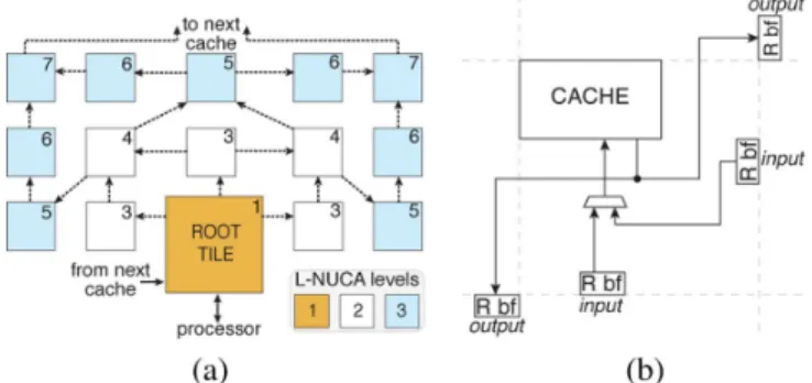
The three networks use point-to-point links between adjacent tiles to minimize link delay and ease scalability—wires that shorten at scaling do not change their relative delay to gates [29]—although each network has a different topology to sat-isfy their different needs. The Search and Transport networks focus on low latency and high bandwidth, while the Replace-ment one focuses on ordering blocks according to temporal lo-cality. In what follows, we explain the networks for a three-level L-NUCA example.
1) Search: As shown in Fig. 4(a), search messages proceed through a broadcast-tree with minimum degree.6This topology ensures that all tiles receive a miss requests on a number of cycles less than or equal to the number of L-NUCA levels, which is three cycles or less in our example.
Search routing is simple yet effective. When a tile receives a request and misses, it forwards the requests to all its child tiles. This “wired” multicast is much simpler than multicast in con-ventional routers because it avoids the complexity of message replication [8]. To simplify the Search network even more, it does not use any flow control mechanism. When a request leaves the r-tile, it proceeds through the rest of tiles in a fixed number of cycles, equaling the number of levels. In the rare case that a tile experiences a hit, and all its transport links are busy, it marks the request with a congestion control bit, and the global 5Cache control signals are generated in the previous cycle of the tile ac-cess with information from both the tile itself and the parent tile in the Search network.
Fig. 5. Transport network topology and its components. (a) 2-D mesh topology. (b) Components.
miss logic retries the access from the r-tile. The remaining three control bits of search messages encode whether the request is a load or a store and, in the latter case, its size (see Table III).
Another key feature for reducing the Search network delay is to couple the router with the cache. As depicted in Fig. 4(b), the Search network is directly connected to the cache and only requires the Miss Address Register (MAR) and STore Data Register (STDR) to save the address and the store data for r-tile write misses. R buffers (R bf) of the Replacement network are included in the lookup, because otherwise either blocks in transit could be overlooked or search operations would have to wait (increasing latency) until the insertion from the R buffers completes.
After looking up all of the L-NUCA tiles, the global miss signal is determined by logically ANDing the miss signals coming from all the last-level tiles. The delay added by the largest wire ending up in the ANDgate does not increase the L-NUCA cycle. Section VI-A on miss-wave stopping elabo-rates more on this issue.
2) Transport: The Search network can inject a new request every cycle, so we can expect bursts of hits to be transported to the r-tile, demanding lots of bandwidth. A 2-D mesh was se-lected for the Transport network [see Fig. 5(a)] because it pro-vides a high bandwidth with its multiple returns paths to the r-tile.
The Transport network follows a distributed routing mech-anism, where each node selects an output link reducing con-gestion; consecutive messages with same origin and destination take a different route on the contrary to dimension-order routing. We have tested random and round-robin allocation policies with good results, making unnecessary more complex policies.
Flow control signals buffer availability with an On/Off protocol. Each buffer stores up to two messages because the round-trip delay between tiles is 2. Larger buffers are undesir-able since they would increase delay, area, and energy. Most importantly, gains would be marginal because the number of in flight misses is limited by the size of the Miss Status Holding Register. Fig. 5(b) depicts the components of the Transport network. Since lookups can hit either in the data cache or in the R buffers, all of them, as well as the tile’s T buffers (T bf) are inputs to the crossbar switch.
Fig. 6. Replacement network topology and its components. Numbers represent the tile latency assuming one-cycle tiles. Tile latency includes search, tile access, and transport delay. (a) Latency-driven topology. (b) Components.
Transport routers are serially accessed after caches, so their delay is critical. Two components make up this delay: the allo-cator and the switch. The first grants outputs to requests, and the second routes the granted inputs to the outputs.
The complexity of the allocator can be reduced based on two architectural observations. First, since cache content among tiles is in exclusion, the lookups in the cache and in the two replace-ment buffers always return zero or one hit. Therefore, only 3 re-questers can be active for the two outputs at maximum. Second, the allocator prioritizes Search (younger) requests that hit in the tile (cache or replacement buffers) over transport buffers (older requests). Otherwise, it would require an extra buffer for the hit and another input port in the allocator to route the hit in a sub-sequent cycle. This priority scheme does not starve requesters because in the worst-case scenario, older requests will proceed when the Miss Status Holding Register becomes full. At that time, the insertion of new misses into the L-NUCA is stopped. Request signals almost drive output grants, which are imple-mented with 5-b one-hot vectors to remove decoding in the con-trol switch. With previous optimizations, the allocator critical path only requires three gate levels with a maximum delay of 0.36 ns. As we will see in Section IV, this delay is sufficiently short to proceed in parallel with the data array access.
3) Replacement: Fig. 6(a) shows the Replacement network. It follows an irregular topology with node degree varying between 2 and 4. Links connect adjacent tiles whose latency (round-trip delay from the r-tile) differs by one cycle (two cycles for links starting in the r-tile) and go in chess king directions.
By following the replacement paths, evicted blocks become ordered in a kind of global LRU list: most recently evicted blocks remains close to the r-tile and the tiles with the highest latency (seven cycles) store less recently evicted blocks. More-over, the Replacement network tries to maintain blocks in the L-NUCA as much as possible; hence, when a level is added, all eviction paths increase their length by three hops.
Replacement takes three nonconsecutive cycles: one to re-ceive an evicted block into the input R buffers [see Fig. 6(b)], another to access the cache for selecting the target way, and the last one to write the block into the target way. During the second cycle, if the selected way contains a valid block, it is
evicted to an output R buffer, and the neighbor tile repeats this “domino-like” operation.
Since transport and replacement are completely decoupled, when a tile hits and the r-tile is full, the chain of evictions may not immediately reach an empty way; it may instead have to evict a block to a higher latency tile. Nevertheless, the global associativity, tile associativity number of tiles, of L-NUCAs is so high that average access time is almost unaffected.
Like the Transport network, the Replacement network uses dynamic routing. However, replacement messages hop only once to reach their destination. When a tile has to evict a block, it selects the output channels with a round-robin policy and writes into the destination buffer without passing through any switch. The choice of the incoming R buffers is done in the same way, via a 2-to-1 multiplexer, as shown in Fig. 6(b).
Finally, L-NUCA networks-in-cache are deadlock-free be-cause the r-tile is always a sink node and there are no cyclic dependencies among messages.
IV. VLSI IMPLEMENTATION
Here, we present an L-NUCA VLSI implementation in order to evaluate three main aspects: complexity, feasibility of wide links, and networks-in-cache overheads in terms of area, power consumption, and timing. The design flow employed the fol-lowing tools: Synopsys Design Compiler (synthesis), Cadence SOC-Encounter (placement and routing), and Mentor Graphics ModelSim (simulation). The technology library is a low-power 90-nm technology available to European universities, featuring nine metal layers.
In each tile, we consider a two-way set associative 32-KB cache with 32-B blocks and least-recently-filled (LRF) replace-ment. LRF works as follows: when a tile receives an evicted block, it evicts the oldest block in the same set or the least re-cently filled one. Parallel access to tag and data arrays is em-ployed to shorten the critical path delay. This is a configuration commonly seen for a first-level cache in the high-end embedded market, except for the associativity, which is usually higher in commercial caches; e.g., four ways in the IBM PowerPC 476FP and eight ways in the Freescale e500mc/e5500 [2], [6]. The Transport and Replacement networks implement round-robin allocation policy because it minimizes area.
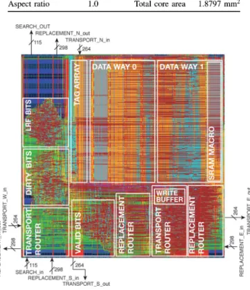
L-NUCAs of any size can be built with two tile types, dif-fering only in the transport network; one for the middle column (three input and one output transport links), and the other one for the rest of tiles (two input and two output transport links). In both designs, most connections match when tiles are placed side by side. Therefore, building an L-NUCA with the desired number of levels is very easy. Since both tile types involve the same design complexity, here we focus on the second and the most common one. Table IV shows a summary of placement and routing statistics and Fig. 7 a layout of a tile located at the left of the r-tile. Note that the layout for a tile to the right of the r-tile can be obtained by mirroring its left counterpart.
The networks-in-cache require 2458 data pins and 40 more to enable permissions and flow control. Each side of a tile contains up to 677 pins routed in M3 and M4 layers.
TABLE IV
PLACEMENT ANDROUTINGSUMMARY
Fig. 7. L-NUCA tile layout with pin placement.
For the cache memory, we chose single-port SRAM macros with 512 entries of 64 b, which can be written at byte granularity. The two cache ways are mapped onto eight SRAM macros, whereas the whole tag directory fits in a single one (assuming 43-b addresses, a tag has 29 b and there are still three free bits to implement an hypothetical coherence protocol). The SRAM macros occupy the largest portion of the tile. The replacement and status bits (LRF, dirty, and valid) are stored in separate flip-flops. This allows trivial multiported access to the tags, for example to invalidate a block sent to the r-tile in the previous cycle while simultaneously probing another access this cycle.
A. Area
Fig. 8 shows the area breakdown by module. The nine SRAM macros of the data and tag array dominate, accounting, respec-tively, for 68% and 8% of the total. The write buffer, valid, LRF, and dirty bits occupy 10%.
The network-in-cache overhead is small, representing only 11% of the total area (5% for the Transport and 6% for the Re-placement network). Even though the Transport router includes the output switch, the Replacement router area is larger because its buffers are bigger and it contains four address comparators and four write mergers for handling load and store hits in the R buffers.
Fig. 8. Main modules area distribution.
Fig. 9. Statistical power distribution.
B. Power
The global static power and the dynamic power for each main module is reported in Fig. 9. The pie chart comes from a statistical-based power distribution assuming an activity factor of 0.2 at the maximum operation frequency and typical case conditions. The total average power is 32.3 mW, comprising 22.67 mW of switching power, 8.89 mW of internal power, and 0.7 mW of leakage, representing only 2% of the total thanks to the used low-power technology.
The cache memory access represents most of the dynamic consumption (53%, including data and tag arrays, LRF, status bits and write buffers), while the Replacement and Transport networks consume only 25%. The cache control logic is mostly responsible of the Rest piece that also includes a small frac-tion due to the Search network (miss propagafrac-tion to the child tiles). This breakdown implies that in order to reduce the overall L-NUCA power it is necessary to reduce the number of tile ac-cesses triggered by r-tile misses. Section VI presents two tech-niques aimed at this objective.
C. Timing
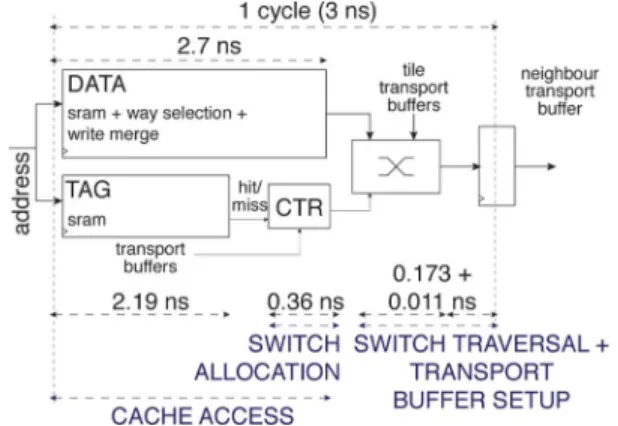
As expected, the longest paths are two: evicting the victim block through the Replacement network and sending the hit block to the transport buffer of a neighbor tile. Fig. 10 shows the second one, which is the critical path.
The critical path closed timing at 3 ns with 0.116 ns of slack. Data delay involves SRAM reading followed by write merging, while tag delay involves SRAM reading followed by address comparison. The data array delivers a block 2.7 ns after the rise of the clock, while the hit/miss signal is available 0.5 ns ear-lier (2.7–2.19). The early arrival of the hit/miss signal enables
Fig. 10. Tile critical path.
switch allocation to occur in parallel with the data access. After allocation, traversing the switch and writing the transport buffer requires 0.173 and 0.011 ns, respectively, accounting for less than 10% of the cycle time.
So, from a practical standpoint, we conclude that the pro-posed networks-in-cache enable both cache-access and single hop routing in one processor cycle.
V. PERFORMANCECOMPARISONS
Here, we describe our detailed simulation environment and compare the performance of the implemented L-NUCA cache with an L2 cache representative of the high-end embedded marked and a Static NUCA (S-NUCA) [7] as a possible low-power alternative.
A. Experimental Framework
We have heavily extended SimpleScalar 3.0d for Alpha [30], including accurate models for Light and Static NUCAs. The baseline processor mimics the two-way out-of-order core of the IBM/LSI PowerPC 476FP [2], [3], [31].
Table V summarizes the simulation parameters for the ref-erence processor and cache hierarchy, including the same L1 and L3 caches and either a conventional L2, a S-NUCA, or an L-NUCA. All caches use LRU replacement except L-NUCA that employs LRF, least-recently-filled, and they all have a single read/write port.
The S-NUCA is organized in a 2 2 2-D mesh with 128-KB banks. This configuration was selected after exploring the S-NUCA design space. Larger number of banks do not improve performance because network overhead becomes very high even if the latency of the wormhole router is set to one processor cycle. Bidirectional links were doubled from the original 16 bytes to 32 to match the size of L-NUCA transport links.
Unfortunately, the latency and the initiation rate of the Pow-erPC 476FP L2 and L3 caches are unknown, so we optimisti-cally estimate them with the High Performance model of Cacti 6.5 [32]. For example, the dedicated L2 of the ARM Cortex-A8 has a cache latency of 6 cycles, 50% larger than our L2 [33]. Additionally, the L2 tag and data arrays are sequentially ac-cessed, as in the PowerPC 476FP, because parallel access does not significantly improve performance; a 0.6% instruction per cycle (IPC) improvement at the cost of increasing dynamic and static energy, 19% and 4.5%, respectively. L2 latency decreases
TABLE V
SIMULATORMICRO-ARCHITECTURALPARAMETERS. BS, AM, LAT,ANDINITSTAND FORBLOCKSIZE, ACCESS
MODE, LATENCY,ANDINITIATIONRATE, RESPECTIVELY
TABLE VI
BENCHMARKSELECTION. THEL1 MPKI CORRESPOND TO THEL1 CACHES OFTABLEV
from four to three cycles, but initiation rate increases from two to three cycles.
Table VI shows the workload selection that includes 13 benchmarks from SPEC CPU2000 and CPU2006 [34], [35]. All of them commonly employed in the embedded domain: gaming, image recognition, or compression. Table VI also includes Misses Per Kilo-Instruction (MPKI) for the L1 cache. MPKI is an useful metric allowing the architect to get an insight on which applications LP-NUCA is expected to show its full potential; those with a higher L1 MPKI fit better to LP-NUCA. Simulations consist of a 100-million instruction run after a warm-up of 200 million instructions following the SimPoint guidelines [36].
Finally, the simulations were also used to validate the L-NUCA HDL description. We extracted memory traces up to
Fig. 11. Performance comparison of L2, S-NUCA, and 3-level L-NUCA. (a) IPC. (b) AMAT.
150 000 references long from the architectural simulator and fed the Verilog simulations to verify the outputs were equal. B. IPC and AMAT Comparison
Fig. 11(a) shows the harmonic mean of Integer and Floating Point IPCs for the reference L2, S-NUCA, and L-NUCA caches. L-NUCA performs better than L2 and S-NUCA regardless of the benchmark group. Gains range among 2.5% to 8.1%. L-NUCA gains are larger in Floating Point benchmarks because their average L1 MPKI doubles that from Integer. L-NUCA improvements are consistent among benchmarks; e.g., they range between 0.5% (458.sjengCINT2006) and 10.3% (179.art CFP2000) relative to the second best configuration, the refer-ence L2. Please note that 458.sjeng and 179.art are among the benchmarks having the lowest and highest L1 MPKI, as shown in Table VI.
Network overhead is the cause behind S-NUCA results. As shown in Section II, S-NUCA network mechanism was designed for large last level multimegabyte caches, and the three required hops per access (on average) double the effective cache latency.
Fig. 11(b) shows the average memory access time (AMAT) for all configurations. Although AMAT combines miss rate, miss penalty, and hit latency, it should be analyzed with care in out-of-order processors because AMAT does not reflect the latency overlap among misses [37]. L-NUCA reduces AMAT about 5% relative to L2 and S-NUCA in both benchmark groups. The IPC and AMAT gains offered by L-NUCA mostly come from hit-and-miss time reductions than from miss rate decrements.
Interestingly, S-NUCA, despite having a lower AMAT, has an IPC worse than L2 in Floating Point benchmarks. Two bench-marks cause this effect: 482.sphinx3 and 177.mesa. S-NUCA IPC decreases 8% and 9.2%, respectively, because the S-NUCA write buffer is filled during a larger fraction of time, stalling the commit of stores even though loads complete faster.
Finally, AMAT differences are larger than their IPC coun-terpart because our processor model exploits memory level parallelism with its out-of-order core and the large Miss Status Holding Registers. With simpler in-order cores, IPC gains would be larger.
VI. LOW-POWERENHANCEMENTS
Here, we describe Light-Power NUCA (LP-NUCA), the improved low-power L-NUCA. Next, it quantifies its dynamic
(a) (b)
Fig. 12. L-NUCA unnecessary accesses after a second level hit and LP-NUCA with a level-2 hit detection gate. (a) Extra accesses in the third level. (b) Hit detection gate between the second and third levels.
energy savings with estimations from the 90-nm VLSI imple-mentation. Finally, in two possible 32-nm application domains, it compares LP-NUCA energy consumption and energy-delay against an L2 cache, representative of the high-end embedded market, and a Static NUCA [7], as another low-power alterna-tive.
Reducing dynamic energy consumption in L-NUCAs re-quires lowering the number of tile accesses. L-NUCA can do thisreactivelyby recognizing and stopping unnecessary activity already in progress, and proactivelyby trying to minimizing activity before it starts. We present one reactive technique, Miss Wave Stopping, and another proactive, Sectoring. They both have low complexity and take advantage of the network organization to save energy without degrading performance. A. Miss Wave Stopping
One source of energy waste is the unnecessary lookups per-formed by the search operation after a hit in a lower level. In the base L-NUCA, tiles do not share hit information, and they only stop miss waves to their child tiles. For example, Fig. 12(a) shows a hit in a level-2 tile. Seven of the nine level-3 tiles look for a block that they surely do not have (because data is exclusive across all tiles and one tile has already hit). These extra lookups can be avoided if tiles propagate the search request only when all the tiles of a level miss. Fortunately, as shown in Fig. 10, hit/miss signals are ready after around two thirds of the tile latency. The remaining time can be used for computing a wave-stop signal by “ORing” all the hit signals of a level. Fig. 12(b) shows a three-level LP-NUCA with a hit detection gate in level 2. When the wave-stop signal is set, all the level-3 tiles discard the search operation.
At first glance, Miss Wave Stopping seems to reduce the mod-ularity and scalability of L-NUCA because it introduces wires that connect multiple tiles. Nevertheless, their length—and delay—scales when technology shrinks [29], and increasing the number of levels beyond 4 does not get additional benefits [18]. So this technique does not increase the complexity of the L-NUCA implementation.
Note that this technique cannot affect performance because the number of hits is the same and, only extra accesses are removed.
B. Sectoring
Sectoring is a proactive technique limiting the activity in the Search and Replacement networks by restricting block place-ment. One end, a cache block can be mapped in a fixed unique
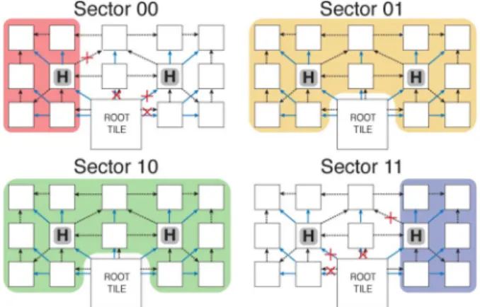
Fig. 13. Three-level sectored LP-NUCA. For each sector, red crosses mark the disabled links in the Search and Replacement networks; “H” tiles have repli-cated the r-tile hash function to ensure blocks do not leave their sector.
NUCA tile, such as in Static NUCA [7]. The other end, blocks can be mapped in any tile such as L-NUCA. Sectoring is in be-tween and maps blocks to clusters of tiles, sector, based on the Search network branches. The idea is similar to the D-NUCA sparse sets [7], but differs in that if sparse sets share a single bank, then all cache banks are -way set associative while the L-NUCA sectors do not impose any restriction on the cache con-figuration. Blocks are mapped to sectors based on a hash func-tion of their addresses. As a simple and efficient hash funcfunc-tion, we use that of the skewed-associative caches [38].
Fig. 13 shows a three-level sectored LP-NUCA with four sec-tors. When the r-tile misses, it hashes the block address to obtain a 2-b sector number. Depending on the value, the search request is propagated to all the second level tiles (sectors 01 and 10), or only to the two tiles on the left (sector 00) or on the right (sector 11). The miss wave propagation proceeds as usual except in the tiles marked with “H”, which compute again the hash function and forward the miss request according to the sector number. In this way, sectors 00 and 11 will experience at most six lookups instead of 14. The r-tile also evicts blocks according to sector number.
Sectoring changes global associativity. For instance, in the implemented 3-level LP-NUCA, we depart from the homo-geneous 28-way set associative structure (tile associativity number of tiles) to end up with different associativities: 28 and 12 for sectors 01–10 and 00–11, respectively. In any case, the associativity is still big, and the key factor for maintaining per-formance is to equally evict blocks among sectors. Assuming the hash function evenly distributes blocks among sectors, the eviction policy has to equalize the traffic among the three replacement links: all 00-blocks leave the r-tile through its West replacement link (West-rl), all 11-blocks through its East-rl, and for the remainder 50% blocks, two thirds are evicted through the North-rl and one third is halved between West-rl and East-rl. The extra hardware for this technique is only a counter and two 3-b flip-flops instead of the current 2-b round-robin flip-flop. C. Energy Estimation in 90 nm
Tile energy consumption is estimated by extracting the post-layout netlist and simulating the tile behavior for at least 1024 consecutive operations with random data. Operations include: read hit, read miss, write hit, write miss, fill with eviction, fill
TABLE VII
SECTORINGIMPACT ONTRAFFICDISTRIBUTION FOR THE
WHOLEWORKLOAD IN ATHREE-LEVELLP-NUCA
without eviction, and transport. Then, for every tile, the average energy per operation is multiplied by the corresponding tile ac-tivity counter, previously obtained with the microarchitectural simulator.
As previously stated, sectoring is an effective technique when it is able to distribute blocks evenly among sectors and reduce tile accesses. Table VII shows the total number of tile accesses for a three-level LP-NUCA with sectoring and an L-NUCA without it. Accesses are reduced by 36.5% and 35.3% for In-teger and Floating Point, respectively. More important, the hash function distributes blocks almost perfectly for Integer bench-marks—a perfect hashing would be 37.5, 25, and 37.5—and a bit worse for Floating Point.
Miss Wave Stopping is effective because most LP-NUCA hits occur in the second level tiles, namely, 78% and 62% for Integer and Floating Point programs. As a consequence, most time only 5 of the 14 tiles perform any activity, and these 5 tiles ensure that the network consumption is low: requests do not propagate to all fabric (Search), hit service only requires one or two hops (Transport), and the empty ways leaved by these hits are im-mediately filed with r-tile evictions stopping the domino effect (Replacement). Finally, although the number of requests to the second level caches is small—on average the r-tile injects a re-quest in three out of 100 cycles—its service latency is crucial in performance because out-of-order cores tolerate the latencies of first level caches but not those of the second one.
LP-NUCA does not hurt performance. On one hand, Miss Wave Stopping cannot affect performance by construction. On the other hand, Sectoring causes a negligible hit ratio reduction, but the extra latency is hidden by out of order execution.
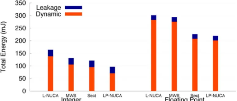
As far as the power consumption of our design is concerned, Fig. 14 shows the results for a baseline L-NUCA, an L-NUCA enhanced with Miss Wave Stopping (MWS), an L-NUCA en-hanced with Sectoring (Sect), and an LP-NUCA that comprises both techniques. The plot represents the sum of the energies spent for all the benchmarks. Each bar represents the leakage consumption stacked over the dynamic, which is the target of our techniques.
MWS is effective whether it applies to L-NUCA or Sectoring. Relative gains in dynamic energy are very similar in both cases, but its effectiveness is larger for the Integer set because these benchmarks exhibit the highest hit ratio, and this technique is useless for misses.
With respect to Sectoring, it saves more energy than Miss Wave Stopping, whether it applies to L-NUCA or MWS. Savings are larger for two reasons. First, it reduces the energy in two operations: search (lookup is performed in fewer tiles), and replacement (blocks pass through fewer tiles to leave the LP-NUCA), while MWS only decreases the search energy.
Fig. 14. LP-NUCA energy savings in 90 nm. L-NUCA represents the original organization, MWS and Sect add miss wave stopping and sectoring, respec-tively, and LP-NUCA combines both.
Second, Sectoring is effective for both hits and misses in contrast with MWS, which only targets hits.
If we look separately at dynamic and static energy, the static contribution is not negligible as one could expect from Fig. 9. Averaging all programs together, the static energy represents 9.4% of the total in the L-NUCA configuration because tile ac-tivity is not very high. For instance, if we assume a r-tile miss rate of 10%, only one in ten cycles there is dynamic consump-tion, whereas leakage is active the ten cycles. Of course, as the dynamic activity decreases, the relative static contribution increases because the execution time is almost constant in all configurations.
Finally, we can consider all programs together to quantify the impact of Wave Miss Stopping and Sectoring on the total en-ergy consumption. With respect to L-NUCA, Miss Wave Stop-ping saves 8.7%, Sectoring saves 25.4%, and their combination, LP-NUCA, rises the savings up to 32.1%.
We do not include any energy measurements regarding the conventional L2 cache and the S-NUCA organization, because we do not have any place & routed designs available for them in our 90-nm implementation technology. Also, mixing real im-plementation measurements with Cacti estimations at 90 nm is not a good option because our 90-nm technology does not match well with the 90-nm technology assumptions of Cacti. Instead, we chose to perform the energy comparison of the three cache organizations under a common framework employing Cacti and 32-nm technology models. Next, the obtained results along with the technology parameters employed are discussed.
D. Technology Scaling to 32 nm
LP-NUCA offers three main advantages over conventional or S-NUCA second level cache organizations. First, its tiled or-ganization allows changing cache size by just replicating the LP-NUCA tiles as many times as needed. The tile’s area, delay, and power characteristics, and thus its scaling to smaller tech-nologies are mainly determined by the size and the character-istics of the SRAM banks inside each tile. For acceptable per-formance, the total SRAM size per tile can be as low as 8 KB [18]. Second, it requires smaller total memory size compared to a conventional or S-NUCA L2 cache in order to perform equally well, in terms of IPC and average memory access time as shown in Fig. 11. From our experiments, equal performance is achieved when the total size of LP-NUCA is 12.5% less than L2 state of the art. Third, the proposed networks-in-cache rely on simple customized switches and on local wire connections, linking only
neighbor tiles. The length of the corresponding wires do not ex-ceed the layout area of the SRAM banks used in each tile. For example, in the 90-nm implementation with 32 KB of SRAM banks the longest inter-tile wires span 1.37 mm.
Two main issues that arise when scaling are wire delay and power consumption. Regarding the former, LP-NUCA is ex-pected to scale well to smaller technologies, assuming a con-stant capacity per tile. All inter-tile wires are short, and their length is solely determined by the area of small SRAM banks used per tile. Therefore, if capacity per tile is sufficiently small, LP-NUCA is guaranteed to behave in terms of latency the same as the 90-nm implementation.
Additionally, if we keep the total cache area constant, in-stead of the total cache size, which is 26.3 mm for a three-level LP-NUCA at 90 nm (r-tile not included), then the empty space left can be filled with more LP-NUCA levels. In this case, in-creased size conventional L2 caches have to face some serious issues arising from long wires [29] that may negatively affect their initiation rate. On the contrary, by construction, the initia-tion rate in LP-NUCA remains constant.
The power consumption of LP-NUCA is also expected to scale well to smaller technologies, assuming again a constant capacity per tile and the same number of tiles. LP-NUCA would benefit from the smaller capacitances offered by smaller de-vices, while at the same time its activity reduction techniques would again reduce any unnecessary power consumption. Also, LP-NUCA implicitly saves static power when compared to con-ventional or S-NUCA caches, since: 1) it provides a similar level of performance with lower cache sizes and 2) it reduces the total execution time [18].
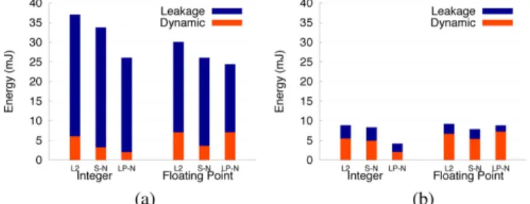
To verify these qualitative arguments, we have simulated an LP-NUCA, a conventional L2, and a S-NUCA at 32 nm using Cacti 6.5, keeping cache sizes constant. At 32 nm, there are a lot of options regarding the operating voltage, the transistor’s threshold as well as the per m current ratio [39]. All of these parameters can be tuned depending on the application domain. For high-performance low-power processors, we can identify two main domains: mains-powered and battery-pow-ered. To the first category, we find high-end networking systems, storage servers, or set-top boxes requiring the maximum perfor-mance with limited power consumption, while the second cat-egory covers systems that are designed for delivering desktop-level performance with very low energy consumption such as smartphones, eReaders, or mobile internet devices.
At 32 nm, for high-performance cores, the voltage ranges be-tween 0.8 and 1 V, the transistor’s threshold is bebe-tween 0.2 and 0.3 V while the per m ratio approaches 15 [39]–[41]. The model of Cacti 6.5 that best matched these cases is the Low Operational Power (LOP) one after increasing the voltage from 0.6 to 0.9 V7 [32]. Therefore, in the mains-powered domain, we employed the modified LOP model, whereas, in the battery-powered domain, the LSTP (Low STandby Power) for the SRAM core and the modified LOP for the rest. In the LSTP model both threshold voltage and ratio are 7When caches operate at a voltage close to 0.5 V, special circuit techniques are required, such the migration from 6T to 8T cells, which would guarantee SRAM cell stability. The high-performance model of Cacti is not used in the compar-isons since it is far more optimistic regarding the threshold voltage scaling and
I current perm relative to current technologies from industry [39]–[41]. At the same time, this model significantly overestimates theI perm current.
Fig. 15. Energy comparison of conventional L2 (L2), static NUCA (S-N), and LP-NUCA (LP-N) in the two application domains at 32 nm. (a) Mains-powered. (b) Battery-powered.
increased in order to guarantee that the static (leakage) power is always around 10%–20% of the total. Since Cacti does not model the proposed networks-in-cache, in order to estimate their consumption we assume the following: 1) tile capacity (32 KB) remains constant and 2) SRAM, logic transistors, and wires scale equally well. Hence, the relative module con-sumption does not change with scaling. Due to scaling, tile and processor frequency increase from 333 MHz to 1.2 GHz and 1 GHz for the mains-powered and the battery-powered domains, respectively. Finally, as a lower bound on the power consumption of the S-NUCA interconnection network we take that of the LP-NUCA transport network.
Fig. 15 shows the total energy consumption of the three cache organizations for the two application domains at 32 nm. LP-NUCA always requires the smallest static power consump-tion regardless the domain due to the reducconsump-tion in the cache size and in the execution time. As far as the total consumption is concerned, in Integer benchmarks, LP-NUCA overpasses L2 and S-NUCA with gains ranging between 23% and 111%. In Floating Point programs, LP-NUCA is the best option in the mains-powered domain, whereas S-NUCA is the best in the battery-powered domain. Although LP-NUCA significantly saves dynamic power of more than 30% in the majority of the Floating Point benchmarks there is one benchmark, 179.art, that stresses the energy behavior of LP-NUCA. This benchmark has the highest L1 MPKI and causes a lot of activity in the intermediate cache level. Its dynamic power represents 50% of the total dynamic power in L2 and S-NUCA organizations, while it reaches 88% in the LP-NUCA case. LP-NUCA reacts well to 179.art demands and services more hits that the L2 and the S-NUCA; however, 93% of them are serviced from the last level tiles.8 Regarding total energy consumption, in both domains, LP-NUCA wastes less energy with gains ranging from 18% to 39%.
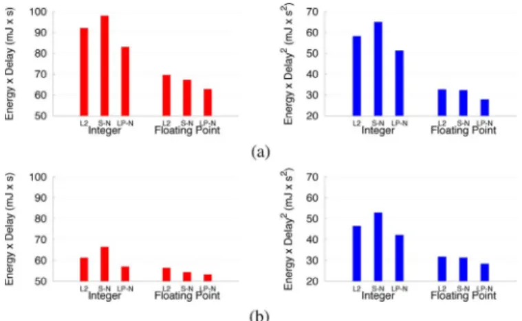
Finally, Fig. 16 compares the three cache organizations using two system level metrics: Energy-Delay (ED) and Energy-Delay ED . Both metrics have been computed by taking the product of the total energy and execution time for all programs together. Please note that the numbers reported in Fig. 16 also include the energy contribution of L1 and L3 caches. With this addition we want to show that even if LP-NUCA reduces the energy of the second level cache, it still 8On average, each hit in 179.art causes 14 tile lookups (both tag and data arrays), transport messages of three hops on average, and four or five domino replacements, all of which increases the overall power consumption.
Fig. 16. ED and ED for the conventional L2 (L2), Static NUCA (S-N), and light power NUCA (LP-N). Both ED and ED comprise level 1, L2 or S-N or LP-N, and level 3 cache energies. (a) Mains-powered. (b) Battery-powered.
does not increase the energy of the remaining cache hierarchy, offering a complete energy-efficient solution.
Fig. 16 shows that LP-NUCA behaves well both in the mains-powered and battery-powered domains, where its sav-ings are larger. LP-NUCA gains are bigger in Integer programs ranging between 2% (battery-powered, Floating Point relative to S-NUCA) and 21% (mains-powered, Integer relative to S-NUCA). Overall, we can conclude that LP-NUCA achieves both better performance and less energy consumption than conventional and S-NUCA caches.
VII. COHERENCEMANAGEMENT ANDREALTIME
A. Coherence Management
Next, we analyze the feasibility of integrating L-NUCA within a multicore chip in a coherent memory system, which essentially does not differ from that of conventional caches. Thereafter, we assume at least one private cache such an L-NUCA inside each core, addressing processor requests, and a single shared last-level cache (LLC) in charge of write serial-ization and coherence handling. The LLC replies to processor requests by issuing corresponding commands accordingly to the content management policy among caches (inclusive, exclusive, noninclusive) and to the scheme for locating cache blocks on cores (from full-map directories to snoopy-like management). These principles are commonly followed by high-end multicore chips.9
An LLC can monitor both the contents of a conventional L1, L2 pair of caches and an L-NUCA. In both cases, the LLC controls block refills and evictions. Thus, regardless of contents management and block location policies, we can focus on the inner management of the external coherence commands entering an L-NUCA cache, such as invalidations, requests for ownership, or remote load misses. These external commands would be a new class of messages in the Search Network, and blocks would be evicted through the Replacement Network 9The shared L2 cache of the UltraSPARC T2 System-on-a-Chip is an ex-ample of an inclusive shared LLC featuring a full-map scheme [42], the shared L2 cache of the low-power ARM Cortex-A9 MPCore processor is an example of snoopy last-level exclusive cache [2], and the shared L3 cache of the third-gener-ation multicore AMD Opteron processors is an example of a noninclusive cache featuring a limited directory scheme [43].
when necessary. In both cases, almost no extra wiring is re-quired, and only the control logic has to be enhanced to process the new coherence messages.
Evaluating the tradeoffs involved in designing a system with coherent L-NUCA is an interesting open work beyond the scope of this paper. From our results, we can guess that coherence traffic should not affect very much the performance of L-NUCA and even may be a cause of further improvement compared to a conventional L1-L2 hierarchy. While on average the Search Network is idle10more than 97% of the time (91% in the worst case, 179.art), the serial L2 cache is idle 83% of the time, not taking into account the write misses refills that do not occur in the LP-NUCA because it is no-write-allocate.
B. Real Time
In multitasking hard real-time systems, all tasks must com-plete execution before their deadlines. In order to perform a schedulability analysis is required to compute the worst case execution time (WCET) of each task and the effects of interfer-ences between tasks as well. Several analysis tools have been proposed to compute useful upper WCET bounds in reasonable time based on modeling the dynamic cache behavior [44]–[46]. Nevertheless, computing tight WCET bounds of real-time ap-plications executing with data cache hierarchies is still an open problem [47].
Regarding modeling their dynamic behavior, L-NUCAs re-semble conventional high-associativity caches, with the added difficulty of the round-robin tile eviction. Sectored LP-NUCAs, by restricting block location may soften the modeling difficulty. Regardless of the modeling tool, two cache features may ease analysis and improve bounds: data locking and partitioning [48], [49].
LP-NUCAs accept in a natural way two partitioning and locking granularities, namely tile and sector. One or more tiles (or a sector) can be devoted to a given task, avoiding (or reducing) inter-task interferences. Furthermore, tiles can be preloaded and locked (at system startup or at context switches) with blocks from one or more tasks. Both partitioning and locking in LP-NUCAs have a negligible hardware complexity and cost. So, we think that LP-NUCAs with partitioning and locking capabilities are good candidates for real-time data caches, and their modeling and experimentation deserve further research.
VIII. CONCLUSIONS
In this paper, we propose, implement, and evaluate light-power NUCA (LP-NUCA), a large distributed victim cache made of small cache tiles. It aims at high-end low-power processors for SoCs and is based on L-NUCA. LP-NUCA lever-ages three specialized networks-in-cache featuring block-wide links for exploiting short-term temporal locality. To prove its feasibility, we have fully implemented a tile in a 90-nm standard-cell based technology, drawing several conclusions.
First, it is very easy to build LP-NUCA with different sizes by just replicating two tile layouts. Second, all of the networks-in-cache proposed in LP-NUCA involve minimum overhead. The area, energy, and delay of LP-NUCAs are dominated by the 10Number of cycles where the Search links between the r-tile and the second level tiles are idle divided by total number of cycles.
SRAM macros filling each tile and not by the interconnection itself. In a 32-B block size, 32-KB tile, LP-NUCA’s low-com-plexity routing and migration policies require 10% of the tile cycle time and 11% of its area and consume at most 25% of the tile power. Third, LP-NUCA introduces two techniques for re-ducing dynamic energy consumption, namely Miss Wave Stop-ping and Sectoring. The former reduces the number of lookups after a hit, and the latter restricts block placement and search.
In order to evaluate performance and energy, we run represen-tative embedded workloads and feed a detailed cycle-by-cycle simulator with the energy costs from the different layout vari-ants in 90 nm and models in 32 nm. Both techniques together decrease the dynamic consumption by one third with regard to L-NUCA without degrading performance. LP-NUCA enables both faster execution and lower energy consumption compared with a slightly larger conventional or S-NUCA L2 cache. Hence, LP-NUCA offers a complete energy-delay efficient solution for high-performance low-power embedded processors.
ACKNOWLEDGMENT
The authors would like to thank B. Greskamp and the staff of CARV-FORTH, particularly G. Passas, and the anonymous reviewers for providing helpful comments on this paper.
REFERENCES
[1] “Intel Xeon Processor C5500/C3500 Series: Datasheet-Volume 1,” Intel Embedded, 2010 [Online]. Available: http://edc.intel.com/Link. aspx?id=3179
[2] T. R. Halfhill, “The rise of licensable SMP,”Microprocessor Rep., vol. 24, no. 2, pp. 11–18, 2010.
[3] “PowerPC Processor (476FP) Embedded Core Product Brief,” LSI Corp., 2010 [Online]. Available: http://www.lsi.com/Distribution-System/AssetDocument/PPC476FP-PB-v7.pdf
[4] “MIPS32 1004K Coherent Processing System (CPS),” MIPS Technol., 2010 [Online]. Available: http://www.mips.com/media/ files/MIPS32_1004K_410.pdf
[5] T. R. Halfhill, “Netlogic broadens XLP family,”Microprocessor Rep., vol. 24, no. 7, pp. 1–11, 2010.
[6] T. R. Halfhill, “Freescale P5 raises QorIQ’s I.Q,”Microprocessor Rep., vol. 24, no. 7, pp. 15–22, 2010.
[7] C. Kim, D. Burger, and S. W. Keckler, “An adaptive, non-uniform cache structure for wire-delay dominated on-chip caches,” inProc. 10th Int. Conf. Architectural Support for Programming Languages and Op-erating Systems (ASPLOS’02), 2002, pp. 211–222.
[8] Y. Jin, E. J. Kim, and K. H. Yum, “A domain-specific on-chip network design for large scale cache systems,” inProc. 13th Int. Symp. High Performance Comput. Architecture (HPCA’07), 2007, pp. 318–327. [9] N. Muralimanohar and R. Balasubramonian, “Interconnect design
con-siderations for large nuca caches,” inProc. 34th Int. Symp. Comput. Architecture (ISCA’07), 2007, pp. 369–380.
[10] N. Muralimanohar, R. Balasubramonian, and N. P. Jouppi, “Op-timizing NUCA organizations and wiring alternatives for large caches with CACTI 6.0,” inProc. 40th Int. Symp. Microarchitecture (MICRO’07), 2007, pp. 3–14.
[11] P. Foglia, D. Mangano, and C. A. Prete, “A nuca model for embedded systems cache design,” inProc. 3rd Workshop Embedded Syst. Real-Time Multimedia (ESTImedia’05), 2005, pp. 41–46.
[12] B. M. Beckmann and D. A. Wood, “Managing wire delay in large chip-multiprocessor caches,” inProc. 37th Int. Symp. Microarchitec-ture (MICRO’04), 2004, pp. 319–330.
[13] S. Cho and L. Jin, “Managing distributed, shared l2 caches through os-level page allocation,” inProc. 39th Int. Symp. Microarchitecture (MICRO’06), 2006, pp. 455–468.
[14] M. Awasthi, K. Sudan, R. Balasubramonian, and J. Carter, “Dynamic hardware-assisted software-controlled page placement to manage ca-pacity allocation and sharing within large caches,” inIn Proc. 15th Int. Symp. High-Performance Comput. Architecture, 2009, pp. 250–261.
[15] M. Chaudhuri, “PageNUCA: Selected policies for page-grain locality management in large shared chip-multiprocessor caches,” inProc. 15th IEEE Int. Symp. High-Performance Comput. Architecture, 2009, pp. 227–238.
[16] N. Hardavellas, M. Ferdman, B. Falsafi, and A. Ailamaki, “Reactive NUCA: Near-optimal block placement and replication in distributed caches,” inProc. 36th Int. Symp. Comput. Architecture (ISCA’09), 2009, pp. 184–195.
[17] J. Merino, V. Puente, P. Prieto, and J. A. Gregorio, “SP-NUCA: A cost effective dynamic non-uniform cache architecture,”SIGARCH Comput. Archit. News, vol. 36, no. 2, pp. 64–71, 2008.
[18] D. Suárez, T. Monreal, F. Vallejo, R. Beivide, and V. Viñals, “Light NUCA: A proposal for bridging the inter-cache latency gap,” inProc. 12th Des., Autom. Test in Europe Conf. and Exhibition (DATE’09), 2009, pp. 530–535.
[19] J. Lira, C. Molina, and A. Gonzalez, “LRU-PEA: A smart replacement policy for non-uniform cache architectures on chip multiprocessors,” inProc. IEEE Int. Conf. Comput. Design, 2009, pp. 275–281. [20] S.-H. Chou, C.-C. Chen, C.-N. Wen, Y.-C. Chan, T.-F. Chen, C.-C.
Wang, and J.-S. Wang, “No cache-coherence: A single-cycle ring in-terconnection for multi-core L1-NUCA sharing on 3-D chips,” inProc. 46th Des. Autom. Conf., 2009, pp. 587–592.
[21] J. Merino, V. Puente, and J. Gregorio, “ESP-NUCA: A low-cost adap-tive non-uniform cache architecture,” inProc. 16th Int. Symp. High Per-formance Comput. Architecture (HPCA’10), 2010, pp. 1–10. [22] N. P. Jouppi, “Improving direct-mapped cache performance by the
ad-dition of a small fully-associative cache and prefetch buffers,” inProc. 17th Int. Symp. Comput. Architecture, 1990, pp. 364–373.
[23] P. Gratz, C. Kim, R. McDonald, S. W. Keckler, and D. Burger, “Im-plementation and evaluation of on-chip network architectures,” inProc. 24th Int. Conf. Comput. Design, 2006, pp. 1625–1628.
[24] J. Lira, C. Molina, and A. González, “The auction: Optimizing banks usage in non-uniform cache architectures,” inProc. 24th Int. Conf. Su-percomputing, 2010, pp. 37–47.
[25] D. W. Plass and Y. H. Chan, “IBM POWER6 SRAM arrays,”IBM J. Res. Devel., vol. 51, no. 6, pp. 747–756, 2007.
[26] R. E. Kessler, R. Jooss, A. Lebeck, and M. D. Hill, “Inexpensive im-plementations of set-associativity,” inProc. 16th Int. Symp. Comput. Architecture, 1989, pp. 131–139.
[27] R. Mullins, A. West, and S. Moore, “Low-latency virtual-channel routers for on-chip networks,” in Proc. 31th Int. Symp. Comput. Architecture, 2004, pp. 188–197.
[28] A. Kumar, P. Kundu, A. P. Singh, L.-S. Pehy, and N. K. Jha, “A 4.6 Tbits/s 3.6 GHz single-cycle noc router with a novel switch allocator in 65 nm CMOS,” inProc. 25th Int. Conf. Comput. Design, 2007, pp. 63–70.
[29] R. Ho, K. W. Mai, and M. A. Horowitz, “The future of wires,”Proc. IEEE, vol. 89, no. 4, pp. 490–504, Apr. 2001.
[30] T. Austin and D. Burger, “SimpleScalar Tutorial (for Tool Set Release 2.0),” SimpleScalar LCC, 1997.
[31] “PowerPC 476FP L2 Cache Core Databook. Version 1.3 Preliminary,”
IBM, 2011.
[32] N. Muralimanohar, R. Balasubramonian, and N. P. Jouppi, “CACTI 6.0: A tool to model large caches,” HP Labs, HP Lab. Tech. Rep. HPL-2009-85, Apr. 2009.
[33] R. Grisenthwaite, “ARM cortex A8 processor,” inProc. IEE Cam-bridge One Day Seminar. Processor Cores Putting Silicon IP to Work, 2005, pp. 1–25.
[34] J. L. Henning, “SPEC CPU2000: Measuring cpu performance in the new millennium,”IEEE Computer, vol. 33, no. 7, pp. 28–35, Jul. 2000. [35] J. L. Henning, “SPEC CPU2006 benchmark descriptions,”SIGARCH
Comput. Archit. News, vol. 34, no. 4, pp. 1–17, 2006.
[36] G. Hamerly, E. Perelman, J. Lau, and B. Calder, “Simpoint 3.0: Faster and more flexible program analysis,” inProc. Workshop Modeling, Benchmarking and Simulation, 2005, pp. 25–30.
[37] J. L. Hennessy and D. A. Patterson, Computer Architecture: A Quanti-tative Approach, 4th ed. San Mateo, CA: Morgan Kaufmann, 2007. [38] A. Seznec, “A case for two-way skewed-associative caches,” inProc.
20th Int. Symp. Comput. Architecture, 1993, pp. 169–178.
[39] M. Bohr, “The new era of scaling in an SoC world,” inDig. Tech. Papers ISSCC, 2009, pp. 23–28.
[40] B. Greeneet al., “High performance 32 nm SOI CMOS with high-k/ metal gate and 0.149 mm SRAM and ultra low-k back end with eleven levels of copper,” inProc. Symp. VLSI Technol., 2009, pp. 140–141. [41] P. Packanet al., “High performance 32 nm logic technology featuring
2nd generation high-k + metal gate transistors,” inProc. Int. Electron Devices Meeting, 2009, pp. 1–4.
![Table VI shows the workload selection that includes 13 benchmarks from SPEC CPU2000 and CPU2006 [34], [35].](https://thumb-us.123doks.com/thumbv2/123dok_us/1662228.2727932/8.891.60.433.633.847/table-shows-workload-selection-includes-benchmarks-spec-cpu.webp)