Converter with Reference Oscillator
AD2S1210
Rev. A
Information furnished by Analog Devices is believed to be accurate and reliable. However, no responsibility is assumed by Analog Devices for its use, nor for any infringements of patents or other
rights of third parties that may result from its use. Specifications subject to change without notice. No One Technology Way, P.O. Box 9106, Norwood, MA 02062-9106, U.S.A.
FEATURES
Complete monolithic resolver-to-digital converter 3125 rps maximum tracking rate (10-bit resolution) ±2.5 arc minutes of accuracy
10-/12-/14-/16-bit resolution, set by user Parallel and serial 10-bit to 16-bit data ports Absolute position and velocity outputs System fault detection
Programmable fault detection thresholds Differential inputs
Incremental encoder emulation
Programmable sinusoidal oscillator on-board Compatible with DSP and SPI interface standards 5 V supply with 2.3 V to 5 V logic interface −40°C to +125°C temperature rating
APPLICATIONS
DC and ac servo motor control Encoder emulation
Electric power steering Electric vehicles
Integrated starter generators/alternators Automotive motion sensing and control
FUNCTIONAL BLOCK DIAGRAM
REFERENCE OSCILLATOR (DAC) EXCITATION OUTPUTS AD2S1210 EN C O D ER EM UL A T IO N SYNTHETIC REFERENCE RESET DATA I/O INPUTS FROM RESOLVER ENCODER EMULATION OUTPUTS VOLTAGE REFERENCE REFERENCE PINS INTERNAL CLOCK GENERATOR CRYSTAL TYPE II
TRACKING LOOP DETECTIONFAULT
FAULT DETECTION OUTPUTS POSITION REGISTER ADC ADC CONFIGURATION REGISTER MULTIPLEXER
DATA BUS OUTPUT
DATA I/O VELOCITY REGISTER 07 467 -00 1 Figure 1.
GENERAL DESCRIPTION
The AD2S1210 is a complete 10-bit to 16-bit resolution tracking resolver-to-digital converter, integrating an on-board program-mable sinusoidal oscillator that provides sine wave excitation for resolvers.
The converter accepts 3.15 V p-p ± 27% input signals, in the range of 2 kHz to 20 kHz on the sine and cosine inputs. A Type II servo loop is employed to track the inputs and convert the input sine and cosine information into a digital representation of the input angle and velocity. The maximum tracking rate is 3125 rps.
PRODUCT HIGHLIGHTS
1. Ratiometric tracking conversion. The Type II tracking loop provides continuous output position data without
conversion delay. It also provides noise immunity and tolerance of harmonic distortion on the reference and input signals.
2. System fault detection. A fault detection circuit can sense loss of resolver signals, out-of-range input signals, input signal mismatch, or loss of position tracking. The fault detection threshold levels can be individually programmed by the user for optimization within a particular application. 3. Input signal range. The sine and cosine inputs can accept
differential input voltages of 3.15 V p-p ± 27%.
4. Programmable excitation frequency. Excitation frequency is easily programmable to a number of standard frequencies between 2 kHz and 20 kHz.
5. Triple format position data. Absolute 10-bit to 16-bit angular position data is accessed via either a 16-bit parallel port or a 4-wire serial interface. Incremental encoder emulation is in standard A-quad-B format with direction output available. 6. Digital velocity output. 10-bit to 16-bit signed digital velocity accessed via either a 16-bit parallel port or a 4-wire serial interface.
TABLE OF CONTENTS
Features ... 1
Applications ... 1
Functional Block Diagram ... 1
General Description ... 1
Product Highlights ... 1
Revision History ... 2
Specifications ... 3
Timing Specifications ... 6
Absolute Maximum Ratings ... 8
ESD Caution ... 8
Pin Configuration and Function Descriptions ... 9
Typical Performance Characteristics ... 11
Resolver Format Signals ... 15
Theory of Operation ... 16
Resolver to Digital Conversion ... 16
Fault Detection Circuit ... 16
On-Board Programmable Sinusoidal Oscillator ... 18
Synthetic Reference Generation ... 18
Configuration of AD2S1210 ... 20
Modes of Operation ... 20
Register Map ... 21
Position Register ... 21
Velocity Register ... 21
LOS Threshold Register ... 21
DOS Overrange Threshold Register ... 21
DOS Mismatch Threshold Register ... 21
DOS Reset Maximum and Minimum Threshold Registers . 22 LOT High Threshold Register ... 22
LOT Low Threshold Register ... 22
Excitation Frequency Register ... 22
Control Register ... 22
Software Reset Register ... 23
Fault Register ... 23 Digital interface ... 24 SOE Input ... 24 SAMPLE Input... 24 Data Format ... 24 Parallel Interface ... 24 Serial Interface ... 28
Incremental Encoder Outputs ... 31
Supply Sequencing and Reset ... 31
Circuit Dynamics ... 32
Loop Response Model ... 32
Sources of Error ... 33
Outline Dimensions ... 34
Ordering Guide ... 34
REVISION HISTORY
2/10—Rev. 0 to Rev. A Changes to Typical Performance Characteristics Section ... 11, 12 Changes to Ordering Guide ... 34 8/08—Revision 0: Initial VersionSPECIFICATIONS
AVDD = DVDD = 5.0 V ± 5%, CLKIN = 8.192 MHz ± 25%, EXC, EXC frequency = 10 kHz to 20 kHz (10-bit); 6 kHz to 20 kHz (12-bit);
3 kHz to 12 kHz (14-bit); 2 kHz to 10 kHz (16-bit); TA = TMIN to TMAX; unless otherwise noted.1
Table 1.
Parameter Min Typ Max Unit Conditions/Comments
SINE, COSINE INPUTS2
Voltage Amplitude 2.3 3.15 4.0 V p-p Sinusoidal waveforms, differential SIN to SINLO,
COS to COSLO
Input Bias Current 8.25 μA VIN = 4.0 V p-p, CLKIN = 8.192 MHz
Input Impedance 485 kΩ VIN = 4.0 V p-p, CLKIN = 8.192 MHz
Phase Lock Range −44 +44 Degrees Sine/cosine vs. EXC output, Control Register D3 = 0
Common-Mode Rejection ±20 arc sec/V 10 Hz to 1 MHz, Control Register D4 = 0
ANGULAR ACCURACY3
Angular Accuracy ±2.5 + 1 LSB ±5 + 1 LSB arc min B, D grades
±5 + 1 LSB ±10 + 1 LSB arc min A, C grades
Resolution 10, 12, 14, 16 Bits No missing codes
Linearity INL 10-bit ±1 LSB B, D grades ±2 LSB A, C grades 12-bit ±2 LSB B, D grades ±4 LSB A, C grades 14-bit ±4 LSB B, D grades ±8 LSB A, C grades 16-bit ±16 LSB B, D grades ±32 LSB A, C grades Linearity DNL ±0.9 LSB Repeatability ±1 LSB VELOCITY OUTPUT Velocity Accuracy4
10-bit ±2 LSB B, D grades, zero acceleration
±4 LSB A, C grades, zero acceleration
12-bit ±2 LSB B, D grades, zero acceleration
±4 LSB A, C grades, zero acceleration
14-bit ±4 LSB B, D grades, zero acceleration
±8 LSB A, C grades, zero acceleration
16-bit ±16 LSB B, D grades, zero acceleration
±32 LSB A, C grades, zero acceleration
Resolution5 9, 11, 13, 15 Bits DYNAMNIC PERFORMANCE Bandwidth 10-bit 2000 6500 Hz 2900 5300 Hz CLKIN = 8.192 MHz 12-bit 900 2800 Hz 1200 2200 Hz CLKIN = 8.192 MHz 14-bit 400 1500 Hz 600 1200 Hz CLKIN = 8.192 MHz 16-bit 100 350 Hz 125 275 Hz CLKIN = 8.192 MHz
Tracking Rate 10-bit 3125 rps CLKIN = 10.24 MHz 2500 CLKIN = 8.192 MHz 12-bit 1250 rps CLKIN = 10.24 MHz 1000 CLKIN = 8.192 MHz 14-bit 625 rps CLKIN = 10.24 MHz 500 CLKIN = 8.192 MHz 16-bit 156.25 rps CLKIN = 10.24 MHz 125 CLKIN = 8.192 MHz Acceleration Error
10-bit 30 arc min At 50,000 rps2, CLKIN = 8.192 MHz
12-bit 30 arc min At 10,000 rps2, CLKIN = 8.192 MHz
14-bit 30 arc min At 2500 rps2, CLKIN = 8.192 MHz
16-bit 30 arc min At 125 rps2, CLKIN = 8.192 MHz
Settling Time 10° Step Input
10-bit 0.6 0.9 ms To settle to within ±2 LSB , CLKIN = 8.192 MHz
12-bit 2.2 3.1 ms To settle to within ±2 LSB, CLKIN = 8.192 MHz
14-bit 6.5 9.0 ms To settle to within ±2 LSB , CLKIN = 8.192 MHz
16-bit 27.5 40 ms To settle to within ±2 LSB, CLKIN = 8.192 MHz
Settling Time 179° Step Input
10-bit 1.5 2.2 ms To settle to within ±2 LSB , CLKIN = 8.192 MHz
12-bit 4.75 6.0 ms To settle to within ±2 LSB, CLKIN = 8.192 MHz
14-bit 10.5 14.7 ms To settle to within ±2 LSB , CLKIN = 8.192 MHz
16-bit 45 66 ms To settle to within ±2 LSB, CLKIN = 8.192 MHz
EXC, EXC OUTPUTS
Voltage 3.2 3.6 4.0 V p-p Load ±100 μA, typical differential output
(EXC to EXC) = 7.2 V p-p
Center Voltage 2.40 2.47 2.53 V
Frequency 2 20 kHz
EXC/EXC DC Mismatch 30 mV
EXC/EXC AC Mismatch 100 mV
THD −58 dB First five harmonics
VOLTAGE REFERENCE
REFOUT 2.40 2.47 2.53 V ±IOUT = 100 μA
Drift 100 ppm/°C
PSRR −60 dB
CLKIN, XTALOUT6
VIL Voltage Input Low 0.8 V
VIH Voltage Input High 2.0 V
LOGIC INPUTS
VIL Voltage Input Low 0.8 V VDRIVE = 2.7 V to 5.25 V
0.7 V VDRIVE = 2.3 V to 2.7 V
VIH Voltage Input High 2.0 V VDRIVE = 2.7 V to 5.25 V
1.7 V VDRIVE = 2.3 V to 2.7 V
IIL Low Level Input Current (Non
Pull-Up)
10 μA
IIL Low Level Input Current (Pull-Up) 80 μA RES0, RES1, RD, WR/FSYNC, A0, A1, and RESET pins
IIH High Level Input Current −10 μA
LOGIC OUTPUTS
VOL Voltage Output Low 0.4 V VDRIVE = 2.3 V to 5.25 V
Parameter Min Typ Max Unit Conditions/Comments POWER REQUIREMENTS AVDD 4.75 5.25 V DVDD 4.75 5.25 V VDRIVE 2.3 5.25 V POWER SUPPLY IAVDD 12 mA IDVDD 35 mA IOVDD 2 mA
1 Temperature ranges are as follows: A, B grades: –40°C to +85°C; C, D grades: –40°C to +125°C. 2 The voltages, SIN, SINLO, COS, and COSLO, relative to AGND, must always be between 0.15 V and AV
DD − 0.2 V. 3 All specifications within the angular accuracy parameter are tested at constant velocity, that is, zero acceleration. 4 The velocity accuracy specification includes velocity offset and dynamic ripple.
5 For example when RES0 = 0 and RES1 = 1, the position output has a resolution of 12 bits. The velocity output has a resolution of 11 bits with the MSB indicating the
direction of rotation. In this example, with a CLKIN frequency of 8.192 MHz the velocity LSB is 0.488 rps, that is, 1000 rps/(211).
6 The clock frequency of the AD2S1210 can be supplied with a crystal, an oscillator, or directly from a DSP/microprocessor digital output. When using a single-ended
AVDD = DVDD = 5.0 V ± 5%, TA = TMIN to TMAX, unless otherwise noted.1
Table 2.
Parameter Description Limit at TMIN, TMAX Unit
fCLKIN Frequency of clock input 6.144 MHz min
10.24 MHz max
tCK Clock period ( = 1/fCLKIN) 98 ns min
163 ns max
t1 A0 and A1 setup time before RD/CS low 2 ns min
t2 Delay CS falling edge to WR/FSYNC rising edge 22 ns min
t3 Address/data setup time during a write cycle 3 ns min
t4 Address/data hold time during a write cycle 2 ns min
t5 Delay WR/FSYNC rising edge to CS rising edge 2 ns min
t6 Delay CS rising edge to CS falling edge 10 ns min
t7 Delay between writing address and writing data 2 × tCK + 20 ns min
t8 A0 and A1 hold time after WR/FSYNC rising edge 2 ns min
t9 Delay between successive write cycles 6 × tCK + 20 ns min
t10 Delay between rising edge of WR/FSYNC and falling edge of RD 2 ns min
t11 Delay CS falling edge to RD falling edge 2 ns min
t12 Enable delay RD low to data valid in configuration mode
VDRIVE = 4.5 V to 5.25 V 37 ns min
VDRIVE = 2.7 V to 3.6 V 25 ns min
VDRIVE = 2.3 V to 2.7 V 30 ns min
t13 RD rising edge to CS rising edge 2 ns min
t14A Disable delay RD high to data high-Z 16 ns min
t14B Disable delay CS high to data high-Z 16 ns min
t15 Delay between rising edge of RD and falling edge of WR/FSYNC 2 ns min
t16 SAMPLE pulse width 2 × tCK + 20 ns min
t17 Delay from SAMPLE before RD/CS low 6 × tCK + 20 ns min
t18 Hold time RD before RD low 2 ns min
t19 Enable delay RD/CS low to data valid
VDRIVE = 4.5 V to 5.25 V 17 ns min
VDRIVE = 2.7 V to 3.6 V 21 ns min
VDRIVE = 2.3 V to 2.7 V 33 ns min
t20 RD pulse width 6 ns min
t21 A0 and A1 set time to data valid when RD/CS low
VDRIVE = 4.5 V to 5.25 V 36 ns min
VDRIVE = 2.7 V to 3.6 V 37 ns min
VDRIVE = 2.3 V to 2.7 V 29 ns min
t22 Delay WR/FSYNC falling edge to SCLK rising edge 3 ns min
t23 Delay WR/FSYNC falling edge to SDO release from high-Z
VDRIVE = 4.5 V to 5.25 V 16 ns min
VDRIVE = 2.7 V to 3.6 V 26 ns min
VDRIVE = 2.3 V to 2.7 V 29 ns min
t24 Delay SCLK rising edge to DBx valid
VDRIVE = 4.5 V to 5.25 V 24 ns min
Parameter Description Limit at TMIN, TMAX Unit
t29 Delay WR/FSYNC rising edge to SDO high-Z 15 ns min
t30 Delay from SAMPLE before WR/FSYNC falling edge 6 × tCK + 20 ns ns min
t31 Delay CS falling edge to WR/FSYNC falling edge in normal mode 2 ns min
t32 A0 and A1 setup time before WR/FSYNC falling edge 2 ns min
t33 A0 and A1 hold time after WR/FSYNC falling edge2
In normal mode, A0 = 0, A1 = 0/1 24 × tCK + 5 ns ns min
In configuration mode, A0 = 1, A1 = 1 8 × tCK + 5 ns ns min
t34 Delay WR/FSYNC rising edge to WR/FSYNC falling edge 10 ns min
fSCLK Frequency of SCLK input
VDRIVE = 4.5 V to 5.25 V 20 MHz
VDRIVE = 2.7 V to 3.6 V 25 MHz
VDRIVE = 2.3 V to 2.7 V 15 MHz
1 Temperature ranges are as follows: A, B grades: –40°C to +85°C; C, D grades: –40°C to +125°C.
2 A0 and A1 should remain constant for the duration of the serial readback. This may require 24 clock periods to read back the 8-bit fault information in addition to the
ABSOLUTE MAXIMUM RATINGS
Table 3. Parameter Rating AVDD to AGND, DGND −0.3 V to +7.0 V DVDD to AGND, DGND −0.3 V to +7.0 V VDRIVE to AGND, DGND −0.3 V to AVDD AVDD toDVDD −0.3 V to +0.3 V AGND to DGND −0.3 V to +0.3 VAnalog Input Voltage to AGND −0.3 V to AVDD + 0.3 V
Digital Input Voltage to DGND −0.3 V to VDRIVE + 0.3 V
Digital Output Voltage to DGND −0.3 V to VDRIVE + 0.3 V
Analog Output Voltage Swing −0.3 V to AVDD + 0.3 V
Input Current to Any Pin Except Supplies1 ±10 mA
Operating Temperature Range (Ambient)
A, B Grades −40°C to +85°C
C, D Grades −40°C to +125°C
Storage Temperature Range −65°C to +150°C
θJA Thermal Impedance2 54°C/W
θJA Thermal Impedance2 15°C/W
RoHS-Compliant Temperature, Soldering Reflow
260(−5/+0)oC
ESD 2 kV HBM
1 Transient currents of up to 100 mA do not cause latch-up. 2 JEDEC 2S2P standard board.
Stresses above those listed under Absolute Maximum Ratings may cause permanent damage to the device. This is a stress rating only; functional operation of the device at these or any other conditions above those indicated in the operational section of this specification is not implied. Exposure to absolute maximum rating conditions for extended periods may affect device reliability.
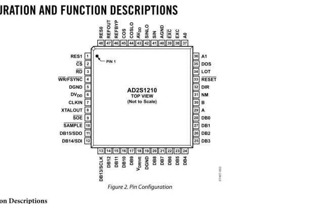
PIN CONFIGURATION AND FUNCTION DESCRIPTIONS
48 RE S 0 47 RE F O U T 46 RE F BY P 45 CO S 44 CO S L O 43 AV DD 42 SI N L O 41 SI N 40 AG ND 39 EX C 38 EX C 37 A0 35 DOS 34 LOT 33 RESET 30 B 31 NM 32 DIR 36 A1 29 A 28 DB0 27 DB1 25 DB3 26 DB2 2 CS 3 RD 4 WR/FSYNC 7 CLKIN 6 DVDD 5 DGND 1 RES1 8 XTALOUT 9 SOE 10 SAMPLE 12 DB14/SDI 11 DB15/SDO 13 DB13/ S C L K 14 DB12 15 DB 11 16 DB10 17 DB9 18 VDR IV E 19 DG ND 20 DB8 21 DB7 22 DB6 23 DB5 24 DB4 PIN 1 AD2S1210 TOP VIEW (Not to Scale) 07 46 7-0 02Figure 2. Pin Configuration
Table 4. Pin Function Descriptions
Pin
No. Mnemonic Description
1 RES1 Resolution Select 1. Logic input. RES1 in conjunction with RES0 allows the resolution of the AD2S1210 to be programmed. Refer to the Configuration of AD2S1210 section.
2 CS Chip Select. Active low logic input. The device is enabled when CS is held low.
3 RD Edge-Triggered Logic Input. When the SOE pin is high, this pin acts as a frame synchronization signal and output
enable for the parallel data outputs, DB15 to DB0. The output buffer is enabled when CS and RD are held low. When the SOE pin is low, the RD pin should be held high.
4 WR/FSYNC Edge-Triggered Logic Input. When the SOE pin is high, this pin acts as a frame synchronization signal and input enable for the parallel data inputs, DB7 to DB0. The input buffer is enabled when CS and WR/FSYNC are held low. When the SOE pin is low, the WR/FSYNC pin acts as a frame synchronization signal and enable for the serial data bus. 5, 19 DGND Digital Ground. These pins are ground reference points for digital circuitry on the AD2S1210. Refer all digital input
signals to this DGND voltage. Both of these pins can be connected to the AGND plane of a system. The DGND and AGND voltages should ideally be at the same potential and must not be more than 0.3 V apart, even on a transient basis. 6 DVDD Digital Supply Voltage, 4.75 V to 5.25 V. This is the supply voltage for all digital circuitry on the AD2S1210. The AVDD and DVDD
voltages ideally should be at the same potential and must not be more than 0.3 V apart, even on a transient basis. 7 CLKIN Clock Input. A crystal or oscillator can be used at the CLKIN and XTALOUT pins to supply the required clock frequency of
the AD2S1210. Alternatively, a single-ended clock can be applied to the CLKIN pin. The input frequency of the AD2S1210 is specified from 6.144 MHz to 10.24 MHz.
8 XTALOUT Crystal Output. When using a crystal or oscillator to supply the clock frequency to the AD2S1210, apply the crystal across the CLKIN and XTALOUT pins. When using a single-ended clock source, the XTALOUT pin should be considered a no connect pin.
9 SOE Serial Output Enable. Logic input. This pin enables either the parallel or serial interface. The serial interface is selected by holding the SOE pin low, and the parallel interface is selected by holding the SOE pin high.
10 SAMPLE Sample Result. Logic input. Data is transferred from the position and velocity integrators to the position and velocity registers, after a high-to-low transition on the SAMPLE signal. The fault register is also updated after a high-to-low transition on the SAMPLE signal.
11 DB15/SDO Data Bit 15/Serial Data Output Bus. When the SOE pin is high, this pin acts as DB15, a three-state data output pin controlled by CS and RD. When the SOE pin is low, this pin acts as SDO, the serial data output bus controlled by CS and WR/FSYNC. The bits are clocked out on the rising edge of SCLK.
12 DB14/SDI Data Bit 14/Serial Data Input Bus. When the SOE pin is high, this pin acts as DB14, a three-state data output pin controlled by CS and RD. When the SOE pin is low, this pin acts as SDI, the serial data input bus controlled by CS and WR/FSYNC. The bits are clocked in on the falling edge of SCLK.
No. Mnemonic Description
13 DB13/SCLK Data Bit 13/Serial Clock. In parallel mode, this pin acts as DB13, a three-state data output pin controlled by CS and RD. In serial mode, this pin acts as the serial clock input.
14 to 17
DB12 to DB9
Data Bit 12 to Data Bit 9. Three-state data output pins controlled by CS and RD.
18 VDRIVE Logic Power Supply Input. The voltage supplied at this pin determines at what voltage the interface operates. Decouple this pin to DGND. The voltage range on this pin is 2.3 V to 5.25 V and may be different to the voltage range at AVDD and DVDD but should never exceed either by more than 0.3 V.
20 DB8 Data Bit 8. Three-state data output pin controlled by CS and RD.
21 to 28
DB7 to DB0 Data Bit 7 to Data Bit 0. Three-state data input/output pins controlled by CS, RD, and WR/FSYNC.
29 A Incremental Encoder Emulation Output A. Logic output. This output is free running and is valid if the resolver format input signals applied to the converter are valid.
30 B Incremental Encoder Emulation Output B. Logic output. This output is free running and is valid if the resolver format input signals applied to the converter are valid.
31 NM North Marker Incremental Encoder Emulation Output. Logic output. This output is free running and is valid if the resolver format input signals applied to the converter are valid.
32 DIR Direction. Logic output. This output is used in conjunction with the incremental encoder emulation outputs. The DIR output indicates the direction of the input rotation and is high for increasing angular rotation.
33 RESET Reset. Logic input. The AD2S1210 requires an external reset signal to hold the RESET input low until VDD is within the specified operating range of 4.75 V to 5.25 V.
34 LOT Loss of Tracking. Logic output. LOT is indicated by a logic low on the LOT pin and is not latched. Refer to the Loss of Position Tracking Detection section.
35 DOS Degradation of Signal. Logic output. Degradation of signal (DOS) is detected when either resolver input (sine or cosine) exceeds the specified DOS sine/cosine threshold or when an amplitude mismatch occurs between the sine and cosine input voltages. DOS is indicated by a logic low on the DOS pin. Refer to the Signal Degradation Detection section.
36 A1 Mode Select 1. Logic input. A1 in conjunction with A0 allows the mode of the AD2S1210 to be selected. Refer to the
Configuration of AD2S1210 section.
37 A0 Mode Select 0. Logic input. A0 in conjunction with A1 allows the mode of the AD2S1210 to be selected. Refer to the
Configuration of AD2S1210 section.
38 EXC Excitation Frequency. Analog output. An on-board oscillator provides the sinusoidal excitation signal (EXC) and its complement signal (EXC) to the resolver. The frequency of this reference signal is programmable via the excitation frequency register.
39 EXC Excitation Frequency Complement. Analog output. An on-board oscillator provides the sinusoidal excitation signal
(EXC) and its complement signal (EXC) to the resolver. The frequency of this reference signal is programmable via the excitation frequency register.
40 AGND Analog Ground. This pin is the ground reference points for analog circuitry on the AD2S1210. Refer all analog input signals and any external reference signal to this AGND voltage. Connect the AGND pin to the AGND plane of a system. The AGND and DGND voltages should ideally be at the same potential and must not be more than 0.3 V apart, even on a transient basis.
41 SIN Positive Analog Input of Differential SIN/SINLO Pair. The input range is 2.3 V p-p to 4.0 V p-p. 42 SINLO Negative Analog Input of Differential SIN/SINLO Pair. The input range is 2.3 V p-p to 4.0 V p-p.
43 AVDD Analog Supply Voltage, 4.75 V to 5.25 V. This pin is the supply voltage for all analog circuitry on the AD2S1210. The AVDD and DVDD voltages ideally should be at the same potential and must not be more than 0.3 V apart, even on a transient basis.
44 COSLO Negative Analog Input of Differential COS/COSLO Pair. The input range is 2.3 V p-p to 4.0 V p-p. 45 COS Positive Analog Input of Differential COS/COSLO Pair. The input range is 2.3 V p-p to 4.0 V p-p.
46 REFBYP Reference Bypass. Connect reference decoupling capacitors at this pin. Typical recommended values are 10 μF and 0.01 μF.
47 REFOUT Voltage Reference Output.
48 RES0 Resolution Select 0. Logic input. RES0 in conjunction with RES1 allows the resolution of the AD2S1210 to be
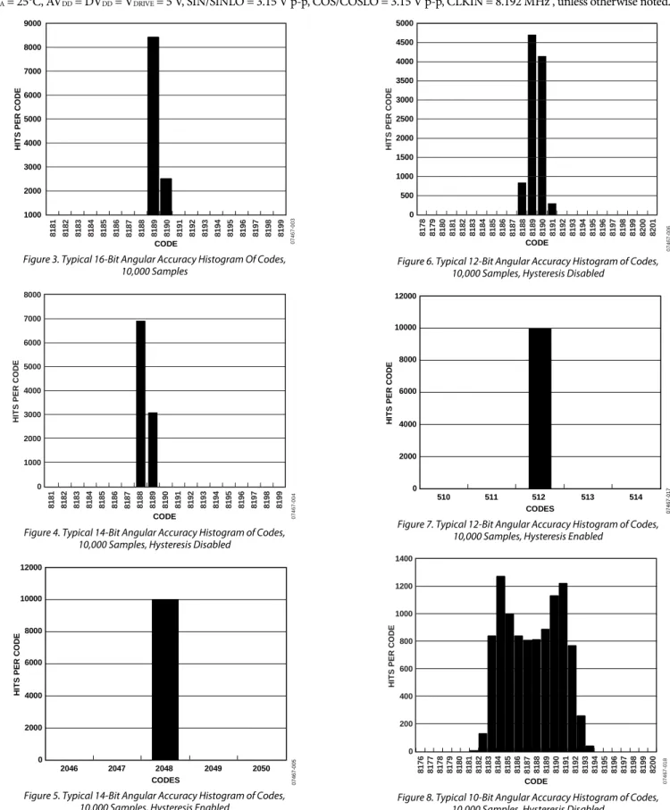
TYPICAL PERFORMANCE CHARACTERISTICS
TA = 25°C, AVDD = DVDD = VDRIVE = 5 V, SIN/SINLO = 3.15 V p-p, COS/COSLO = 3.15 V p-p, CLKIN = 8.192 MHz , unless otherwise noted.
8181 8182 8183 8184 8185 8186 8187 8188 8189 8190 8191 8192 8193 8194 8195 8196 8197 8198 8199 07 46 7-0 03 1000 2000 3000 4000 5000 6000 7000 8000 9000 HI T S P E R CO DE CODE
Figure 3. Typical 16-Bit Angular Accuracy Histogram Of Codes, 10,000 Samples 8000 7000 6000 5000 4000 3000 2000 1000 0 818 1 818 2 818 3 818 4 818 5 818 6 8187 818 8 818 9 819 0 819 1 819 2 819 3 819 4 819 5 819 6 819 7 819 8 819 9 HI T S P E R CO DE 07 46 7-0 04 CODE
Figure 4. Typical 14-Bit Angular Accuracy Histogram of Codes, 10,000 Samples, Hysteresis Disabled
12000 10000 8000 6000 4000 2000 0 2046 2047 2048 2049 2050 CODES H IT S P E R CO DE 07 46 7-00 5
Figure 5. Typical 14-Bit Angular Accuracy Histogram of Codes, 10,000 Samples, Hysteresis Enabled
81 78 81 79 81 80 81 81 81 82 81 83 81 84 81 85 81 86 8187 81 88 81 89 81 90 81 91 81 92 81 93 81 94 81 95 81 96 81 97 81 98 81 99 82 00 82 01 HI T S P E R CO DE 0 74 67 -006 CODE 0 500 1000 1500 2000 2500 3000 3500 4000 4500 5000
Figure 6. Typical 12-Bit Angular Accuracy Histogram of Codes, 10,000 Samples, Hysteresis Disabled
12000 10000 8000 6000 4000 2000 0 510 511 512 513 514 CODES H IT S P E R CO DE 07 46 7-01 7
Figure 7. Typical 12-Bit Angular Accuracy Histogram of Codes, 10,000 Samples, Hysteresis Enabled
1400 1200 1000 800 600 400 200 0 817 8 817 9 817 6 817 7 818 0 818 1 818 2 818 3 818 4 818 5 818 6 8 187 818 8 818 9 819 0 819 1 819 2 819 3 819 4 819 5 819 6 819 7 819 8 819 9 820 0 HI T S P E R C O DE 07 46 7-0 18 CODE
Figure 8. Typical 10-Bit Angular Accuracy Histogram of Codes, 10,000 Samples, Hysteresis Disabled
10000 8000 6000 4000 2000 0 126 127 128 129 130 CODES H IT S P E R CO DE 07 46 7-03 8
Figure 9. Typical 10-Bit Angular Accuracy Histogram of Codes, 10,000 Samples, Hysteresis Enabled
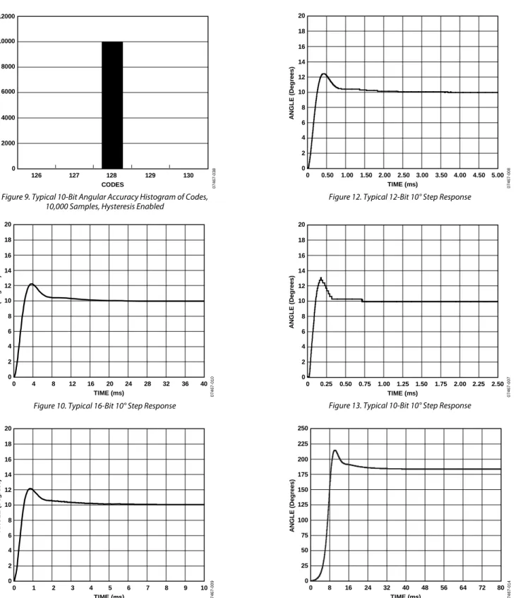
20 18 16 14 12 10 8 6 4 2 0 0 4 8 12 16 20 24 28 32 36 40 TIME (ms) A N G L E ( D eg rees) 07 46 7-0 10
Figure 10. Typical 16-Bit 10° Step Response
20 18 16 14 12 10 8 6 4 2 0 0 1 2 3 4 5 6 7 8 9 10 TIME (ms) A N G L E ( D eg rees) 07 46 7-00 9
Figure 11. Typical 14-Bit 10° Step Response
18 16 14 12 10 8 6 4 2 0 0 0.50 1.00 1.50 2.00 2.50 3.00 3.50 4.00 4.50 5.00 TIME (ms) A N G L E ( D eg rees) 07 46 7-0 08
Figure 12. Typical 12-Bit 10° Step Response
20 18 16 14 12 10 8 6 4 2 0 0 0.25 0.50 0.75 1.00 1.25 1.50 1.75 2.00 2.25 2.50 TIME (ms) ANG L E ( D eg rees) 07 46 7-00 7
Figure 13. Typical 10-Bit 10° Step Response
250 225 200 175 150 125 100 75 50 25 0 0 8 16 24 32 40 48 56 64 72 80 TIME (ms) ANG L E ( D eg rees) 07 46 7 -01 4
250 225 200 175 150 125 100 75 50 25 0 0 2 4 6 8 10 12 14 16 18 20 TIME (ms) ANG L E ( D eg re es ) 07 46 7-0 13
Figure 15. Typical 14-Bit 179° Step Response
250 225 200 175 150 125 100 75 50 25 0 0 1 2 3 4 5 6 7 8 9 10 TIME (ms) ANG L E ( D eg rees) 07 46 7 -01 2
Figure 16. Typical 12-Bit 179° Step Response
250 225 200 175 150 125 100 75 50 25 0 0 1 2 3 4 TIME (ms) ANG L E ( D eg re es) 07 46 7-01 1 5
Figure 17. Typical 10-Bit 179° Step Response
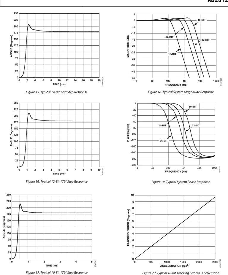
5 0 –5 –10 –15 –20 –25 –30 –35 –40 –45 1 10 100 1k 10k 100k FREQUENCY (Hz) M AG NI T UDE ( d B) 07 46 7 -01 5 16-BIT 14-BIT 12-BIT 10-BIT
Figure 18. Typical System Magnitude Response
0 –40 –20 –60 –80 –100 –120 –140 –160 –180 –200 1 10 100 1k 10k 100k F RE Q U EN CY (H z) PH AS E ( D egr ee s) 07467 -016 16-B IT 14-B IT 12-BIT 10-B IT
Figure 19. Typical System Phase Response
10 8 9 7 6 5 4 3 2 1 0 0 500 1000 1500 2000 2500 ACCELERATION (rps2) T RACKI NG E R RO R ( D eg rees) 07 46 7 -02 2
8 9 7 6 5 4 3 2 1 0 0 5000 10000 15000 20000 25000 30000 35000 40000 45000 ACCELERATION (rps2) T RACKI NG E R RO R ( D eg rees) 07 46 7 -02 1
Figure 21. Typical 14-Bit Tracking Error vs. Acceleration
10 8 9 7 6 5 4 3 2 1 0 0 20000 60000 100000 140000 180000 ACCELERATION (rps2) T RACKI NG E R RO R ( D eg rees) 07 46 7 -02 0
Figure 22. Typical 12-Bit Tracking Error vs. Acceleration
8 9 7 6 5 4 3 2 1 0 0 200000 400000 600000 800000 1000000 ACCELERATION (rps2) T RACKI NG E R RO R ( D eg rees) 07 46 7 -01 9
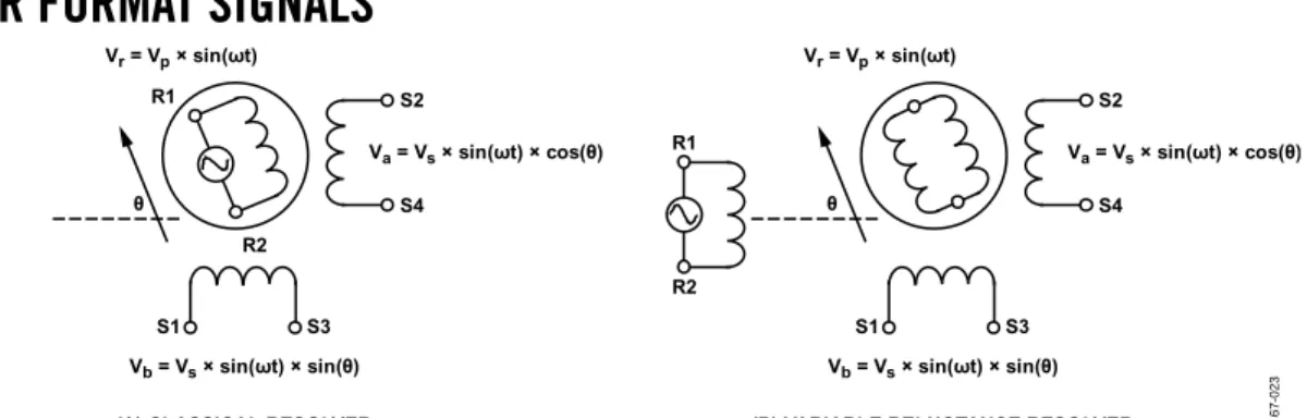
RESOLVER FORMAT SIGNALS
07 46 7-0 23 Vr = Vp × sin(ωt) Vb = Vs × sin(ωt) × sin(θ)(A) CLASSICAL RESOLVER
S1 S3 Va = Vs × sin(ωt) × cos(θ) S2 S4 R1 R2 θ Vr= Vp× sin(ωt) Vb = Vs × sin(ωt) × sin(θ)
(B) VARIABLE RELUCTANCE RESOLVER
S1 S3 Va = Vs × sin(ωt) × cos(θ) S2 S4 R1 R2 θ
Figure 24. Classical Resolver vs. Variable Reluctance Resolver
A resolver is a rotating transformer, typically with a primary winding on the rotor and two secondary windings on the stator. In the case of a variable reluctance resolver, there are no wind-ings on the rotor, as shown in Figure 24. The primary winding is on the stator as well as the secondary windings, but the saliency in the rotor design provides the sinusoidal variation in the secondary coupling with the angular position. Either way, the resolver output voltages (S3 − S1, S2 − S4) have the same equations, as shown in Equation 1.
θ ω θ ω cos sin 4 2 sin sin 1 3 × = − × = − t E S S t E S S 0 0 (1) where:
θ is the shaft angle.
Sinωt is the rotor excitation frequency. E0 is the rotor excitation amplitude.
The stator windings are displaced mechanically by 90° (see Figure 24). The primary winding is excited with an ac reference. The amplitude of subsequent coupling onto the stator secondary windings is a function of the position of the rotor (shaft) relative to the stator. The resolver, therefore, produces two output voltages (S3 − S1, S2 − S4) modulated by the sine and cosine of shaft angle. Resolver format signals refer to the signals derived from the output of a resolver, as shown in Equation 1. Figure 25 illustrates the output format.
07 46 7-0 24 0° S2 – S4 (cos) S3 – S1 (sin) R2 – R4 (REF) 90° 180° θ 270° 360°
THEORY OF OPERATION
RESOLVER TO DIGITAL CONVERSION
The AD2S1210 operates on a Type II tracking closed-loop principle. The output continually tracks the position of the resolver without the need for external conversion and wait states. As the resolver moves through a position equivalent to the least significant bit weighting, the output is updated by one LSB.
The converter tracks the shaft angle θ by producing an output angle ϕ that is fed back and compared to the input angle θ, and the resulting error between the two is driven towards 0 when the converter is correctly tracking the input angle. To measure the error, S3 − S1 is multiplied by cosϕ and S2 − S4 is multiplied by sinϕ to give φ θ ω sin cos sin 0 t× E (for S3 − S1) φ θ ω cos sin sin 0 t× E (for S2 − S4)
The difference is taken, giving
) sin cos cos (sin sin 0 ωt× θ φ− θ φ E (2)
This signal is demodulated using the internally generated synthetic reference, yielding
) sin cos cos (sin 0 θ φ− θ φ E (3)
Equation 3 is equivalent to E0sin(θ − ϕ), which is approximately
equal to E0(θ − ϕ) for small values of θ − ϕ, where θ − ϕ =
angular error.
The value E0 (θ − ϕ) is the difference between the angular error
of the rotor and the digital angle output of the converter. A phase-sensitive demodulator, some integrators, and a compensa-tion filter form a closed-loop system that seeks to null the error signal. When this is accomplished, ϕ equals the Resolver Angle θ within the rated accuracy of the converter. A Type II tracking loop is used so that constant velocity inputs can be tracked without inherent error.
FAULT DETECTION CIRCUIT
The AD2S1210 fault detection circuit can sense loss of resolver signals, out-of-range input signals, input signal mismatch, or loss of position tracking; however, in the event of a fault, the position indicated by the AD2S1210 may differ significantly from the actual shaft position of the resolver.
Monitor Signal
The AD2S1210 generates a monitor signal by comparing the angle in the position register to the incoming sine and cosine signals from the resolver. The monitor signal is created in a similar fashion to the error signal described in the Resolver to
φ θ φ
θ sin 2 cos cos
sin
1× × + × ×
=A A
Monitor (4)
where:
A1 is the amplitude of the incoming sine signal (A1 × sinθ). A2 is the amplitude of the incoming cosine signal (A2 × cosθ). θ is the resolver angle.
ϕ is the angle stored in the position register.
Note that Equation 4 is shown after demodulation, with the Carrier Signal sinωt removed. Also, note that for matched input signal (that is, a no fault condition), A1 = A2.
When A1 = A2 and the converter is tracking (θ = ϕ), the monitor signal output has a constant magnitude of A1 (Monitor = A1 × (sin2 θ + cos2 θ) = A1), which is independent of shaft
angle. When A1 ≠ A2, the monitor signal magnitude varies between A1 and A2 at twice the rate of shaft rotation. The monitor signal is used as described in the following sections to detect degradation or loss of input signals.
Loss of Signal Detection
The AD2S1210 indicates that a loss of signal (LOS) has occurred for four separate conditions.
• When either resolver input (sine or cosine) falls below the specified LOS sine/cosine threshold. This threshold is defined by the user and is set by writing to the internal register, Address 0x88 (see the Register Map section). • When any of the resolver input pins (SIN, SINLO, COS, or
COSLO) are disconnected from the sensor.
• When any of the resolver input pins (SIN, SINLO, COS, or COSLO) are clipping the power rail or ground rail of the AD2S1210. Refer to the Sine/Cosine Input Clipping section. • When a configuration parity error has occurred. Refer to
the Configuration Parity Error section.
A loss of signal is caused if either of the stator windings of the resolver (sine or cosine) are open circuit or have a number of shorted turns. LOS is indicated by both the DOS and LOT pins latching as logic low outputs. The DOS and LOT pins are reset to a no fault state when the user enters configuration mode and reads the fault register. The LOS condition has priority over both the DOS and LOT conditions, as shown in Table 6. To determine the cause of the LOS fault detection, the user must read the fault register, Address 0xFF (see the Register Map section). When a loss of signal is detected due to the resolver inputs (sine or cosine) falling below the specified LOS sine/cosine threshold, the electrical angle through which the resolver may rotate before the LOS can be detected by the AD2S1210 is referred to as the LOS angular latency. This is defined by the specified LOS sine/ cosine threshold set by the user and the maximum amplitude of
Angular Latency = ⎥ ⎥ ⎦ ⎤ ⎢ ⎢ ⎣ ⎡ × amplitude cosine sine threshold LOS Arc / max cos 2 (5)
The preceding equation is based on the worst-case angular error, which can be seen by the AD2S1210 before an LOS fault is indicated. This occurs if one of the resolver input signals, either sine or cosine, is lost while the remaining signal is at its peak amplitude, for example, if the sine input is lost while the input angle is 90°. The worst-case angular latency is twice the worst-case angular error.
Signal Degradation Detection
The AD2S1210 indicates that a degradation of signal (DOS) has occurred for two separate conditions.
• When either resolver input (sine or cosine) exceeds the specified DOS sine/cosine threshold. This threshold is defined by the user and is set by writing to the internal register, Address 0x89 (see the Register Map section). • When the amplitudes of the input signals, sine and cosine,
mismatch by more than the specified DOS sine/cosine mismatch threshold. This threshold is defined by the user and is set by writing to the internal register, Address 0x8A (see the Register Map section). The AD2S1210 continuously stores the minimum and maximum magnitude of the moni-tor signal in internal registers. The difference between the minimum and maximum is calculated to determine if a DOS mismatch has occurred. The initial values for the minimum and maximum internal registers must be defined by the user, at Address 0x8C and Address 0x8B, respectively (see the Register Map section).
DOS is indicated by a logic low on the DOS pin. When DOS is indicated, the output is latched low until the user enters configura-tion mode and reads the fault register. The DOS condiconfigura-tion has priority over the LOT condition, as shown in Table 6. To deter-mine the cause of the DOS fault detection, the user must read the fault register, Address 0xFF (see the Register Map section).
Time Latency for LOS and DOS Detection
Note that the monitor signal is generated on the active edge of the internal AD2S1210 clock. The internal clock is generated by dividing the externally applied CLKIN frequency by 2; for example, when using a CLKIN frequency of 8.192 MHz the internal AD2S1210 clock is 4.096 MHz. The AD2S1210 conti-nuously stores the minimum and maximum magnitude of the monitor signal in internal registers. The values stored in these internal registers are compared to the LOS and DOS thresholds configured by the user at set intervals. This interval, known as the window counter period, is dependent on the excitation frequency configured by the user. It is set to ensure that two window counter periods include at least one full period of the excitation frequency applied to the resolver. The window counter period is defined in terms of internal clock cycles. The
window counter periods for the range of excitation frequencies on the AD2S1210 are outlined in Table 5.
Table 5. Window Counter Period vs. Excitation Frequency Range, CLKIN = 8.192 MHz Excitation Frequency Range Number of Internal Clock Cycles Window Counter Period (μs)1 2 kHz ≤ Exc Freq < 4 kHz 1065 260 4 kHz ≤ Exc Freq < 8 kHz 554 135.25 8 kHz ≤ Exc Freq ≤ 20 kHz 256 62.5
1 CLKIN = 8.192 MHz. The window counter period scales with clock frequency
and can be calculated by multiplying the number of internal clock cycles by the period of the internal clock frequency, that is, CLKIN/2.
The AD2S1210 detects an LOS or DOS due to the resolver inputs (sine or cosine) falling below or exceeding the LOS and DOS thresholds within two window counter periods. For example, with an excitation frequency of 10 kHz, a fault is detected within 125 μs. A persistent fault is detected within one window counter period of the reading and clearing the fault register.
Note that the time latency to detect the occurrence of a DOS mismatch fault is dependent on the speed of rotation of the resolver. The worst-case time latency to detect a DOS mismatch fault is the time required for one full rotation of the resolver.
Loss of Position Tracking Detection
The AD2S1210 indicates that a loss of tracking (LOT) has occurred when
• The internal error signal of the AD2S1210 has exceeded the specified angular threshold. This threshold is defined by the user and is set by writing to the internal register, Address 0x8D (see the Register Map section).
• The input signal exceeds the maximum tracking rate. The maximum tracking rate depends on the resolution defined by the user and the CLKIN frequency.
LOT is indicated by a logic low on the LOT pin and is not latched. LOT has hysteresis and is not cleared until the internal error signal is less than the value defined in the LOT low threshold register, Address 0x8E (see the Register Map section). When the maximum tracking rate is exceeded, LOT is cleared only if the velocity is less than the maximum tracking rate and the internal error signal is less than the value defined in the LOT low threshold register. LOT can be indicated for step changes in position (such as after a RESET signal is applied to the AD2S1210). It is also useful as a built-in test to indicate that the tracking converter is functioning properly. The LOT condition has lower priority than both the DOS and LOS conditions, as shown in
. The LOT and DOS conditions cannot be indicated using the LOT and DOS pins at the same time. However, both condi-tions are indicated separately in the fault register. To determine the cause of the LOT fault detection, the user must read the fault register, Address 0xFF (see the section).
Table 6
Condition DOS Pin LOT Pin
Order of Priority
Loss of Signal (LOS) 0 0 1
Degradation of Signal (DOS) 0 1 2
Loss of Tracking (LOT) 1 0 3
No Fault 1 1 N/A
Sine/Cosine Input Clipping
The AD2S1210 indicates that a clipping error has occurred if any of the resolver input pins (SIN, SINLO, COS, or COSLO) are clipping the power rail or ground rail of the AD2S1210. The clipping fault is indicated if the input amplitudes are less than 0.15 V or greater then AVDD − 0.2 V for more than 4 μs.
Sine/cosine input clipping error is indicated by both the DOS and LOT pins latching as logic low outputs. Sine/cosine input clipping error is also indicated by Bit D7 of the fault register being set high. The DOS and LOT pins are reset to a no fault state when the user enters configuration mode and reads the fault register.
Configuration Parity Error
The AD2S1210 includes a number of user programmable registers that allow the user to configure the part. Each read/write register on the AD2S1210 is programmed with seven bits of informa-tion by the user. The 8th bit is reserved as a parity error bit. In
the event that the data within these registers becomes corrupted, the AD2S1210 indicates that a configuration parity error has occurred. Configuration parity error is indicated by both the DOS and LOT pins latching as logic low outputs. Configuration parity error is also indicated by Bit D0 of the fault register being set high. In the event that a parity error occurs, it is recommended that the user reset the part using the RESET pin.
Phase Lock Error
The AD2S1210 indicates that a phase lock error has occurred if the difference between the phase of the excitation frequency and the phase of the sine and cosine signals exceeds the specified phase lock range. Phase lock error is indicated by a logic low on the LOT pin and is not latched. Phase lock error is also indicated by Bit D1 of the fault register being set high.
ON-BOARD PROGRAMMABLE SINUSOIDAL
OSCILLATOR
An on-board oscillator provides the sinusoidal excitation signal (EXC) to the resolver as well as its complemented signal (EXC). The frequency of this reference signal is programmable to a number of standard frequencies between 2 kHz and 20 kHz. The amplitude of this signal is 3.6 V p-p and is centered on 2.5 V. The reference excitation output of the AD2S1210 needs an external buffer amplifier to provide gain and the additional current to drive a resolver.
signal that is phase locked to its sine and cosine inputs. Phase errors between the resolver primary and secondary windings can degrade the accuracy of the RDC and are compensated by this synchronous reference signal. This also compensates the phase shifts due to temperature and cabling and eliminates the need of an external preset phase compensation circuit.
SYNTHETIC REFERENCE GENERATION
When a resolver undergoes a high rotation rate, the RDC tends to act as an electric motor and produces speed voltages, along with the ideal sine and cosine outputs. These speed voltages are in quadrature to the main signal waveform. Moreover, nonzero resistance in the resolver windings causes a nonzero phase shift between the reference input and the sine and cosine outputs. The combination of speed voltages and phase shift causes a track-ing error in the RDC that is approximated by
Frequency Reference Rate Rotation Shift Phase Error= × (6)
To compensate for the described phase error between the resolver reference excitation and the sine/cosine signals, an internal synthetic reference signal is generated in phase with the refer-ence frequency carrier. The synthetic referrefer-ence is derived using the internally filtered sine and cosine signals. It is generated by determining the zero crossing of either the sine or cosine (whichever signal is larger, to improve phase accuracy) and evaluating the phase of the resolver reference excitation. The synthetic reference reduces the phase shift between the refer-ence and sine/cosine inputs to less than 10°, and operates for phase shifts of ±44°. If additional phase lock range is required, Bit D5 in the control register can be set to zero to expand the phase lock range to 360° (see the Control Register section).
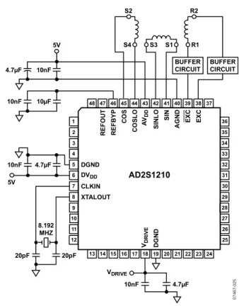
CONNECTING THE CONVERTER
Ground is connected to the AGND and DGND pins (see Figure 26). A positive power supply (VDD) of 5 V dc ± 5% is
connected to the AVDD and DVDD pins, with typical values for the
decoupling capacitors being 10 nF and 4.7 μF. These capacitors are then placed as close to the device pins as possible and are connected to both AVDD and DVDD. The VDRIVE pin is connected
to the supply voltage of the microprocessor. The voltage applied to the VDRIVE input controls the voltage of the parallel and serial
interfaces. VDRIVE can be set to 5 V, 3 V, or 2.5 V. Typical values
for the VDRIVE decoupling capacitors are 10 nF and 4.7 μF.
Typical values for the oscillator decoupling capacitors are 20 pF, whereas typical values for the reference decoupling capacitors are 10 nF and 10 μF.
48 47 RE F O UT 46 RE F BY P 45 CO S 44 CO S L O 43 AV DD 42 SI N L O 41 SI N 40 AG ND 39 EX C 38 EX C 37 35 34 33 30 31 32 36 29 28 27 25 26 2 3 4 7 CLKIN 6 DVDD 5 DGND 1 8 XTALOUT 9 10 12 11 13 14 15 16 17 18 VDRI V E 19 DG ND 20 21 22 23 24 AD2S1210 07 46 7-02 5 20pF 20pF 8.192 MHZ 4.7µF 10nF 5V 5V 10nF 10µF 4.7µF 10nF BUFFER CIRCUIT BUFFER CIRCUIT S2 R2 S4 S3 S1 R1 10nF VDRIVE 4.7µF
Figure 27 shows a suggested buffer circuit. Capacitor C1 may be used in parallel with Resistor R2 to filter out any noise that may exist on the EXC and EXC outputs. Care should be taken when selecting the cutoff frequency of this filter to ensure that phase shifts of the carrier caused by the filter do not exceed the phase lock range of the AD2S1210.
The gain of the circuit is
)) 1 /( 1 ( ) / (R2 R1 R2 C1 ω Gain Carrier =− × + × × (7) and IN REF OUT V C1 R2 R1 R2 R1 R2 V V ⎟ ⎠ ⎞ ⎜ ⎝ ⎛ × × + × ⎟ ⎠ ⎞ ⎜ ⎝ ⎛ − ⎟ ⎠ ⎞ ⎜ ⎝ ⎛ ⎟ ⎠ ⎞ ⎜ ⎝ ⎛ + × = ω 1 1 1 (8) where:
ω is the radian frequency of the applied signal.
VREF, a dc voltage, is set so that VOUT is always a positive value,
eliminating the need for a negative supply. C1 R2 R1 12V 12V 5V EXC/EXC (VIN) (VREF) VOUT 07 46 7-02 6 AD8662 Figure 26. Connecting the AD2S1210 to a Resolver
In this recommended configuration, the converter introduces a VREF/2 offset in the SIN, SINLO, COS, and COSLO signal outputs
from the resolver. The sine and cosine signals can each be connected to a different potential relative to ground if the sine and cosine signals adhere to the recommended specifications. Note that because the EXC and EXC outputs are differential, there is an inherent gain of 2×.
Figure 27. Buffer Circuit
A separate screened twisted pair cable is recommended for the analog input pins, SIN, SINLO, COS, and COSLO. The screens should terminate to either REFOUT or AGND.
CONFIGURATION OF AD2S1210
MODES OF OPERATION
The AD2S1210 has two modes of operation: configuration mode and normal mode. The configuration mode is used to program the registers that set the excitation frequency, the resolution, and the fault detection thresholds of the AD2S1210. Configuration mode is also used to read back the information in the fault register. The data in the position and velocity registers can also be read back while in configuration mode. The AD2S1210 can be operated entirely in configuration mode or, when the initial configuration is completed, the part can be taken out of configuration mode and operated in normal mode. When operating in normal mode, the data outputs can provide angular position or angular velocity data. The A0 and A1 inputs are used to determine whether the AD2S1210 is in configuration mode and to determine whether the position or velocity data is supplied to the output pins, see Table 8.
Setting the Excitation Frequency
The excitation frequency of the AD2S1210 is set by writing a frequency control word to the excitation frequency register, Address 0x91 (see the Register Map section).
(
)
15 2 CLKIN f FCW Frequency Excitation = ×where FCW is the frequency control word and fCLKIN is the clock
frequency of the AD2S1210.
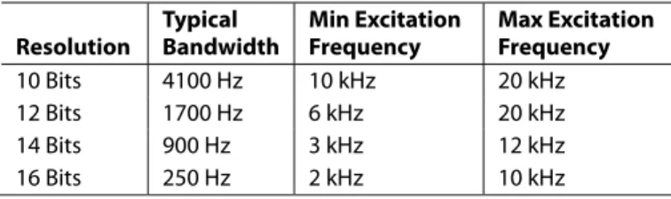
The specified range of the excitation frequency is from 2 kHz to 20 kHz and can be set in increments of 250 Hz. To achieve the angular accuracy specifications in Table 1, the excitation frequency should be selected as outlined in Table 7.
Table 7. Recommended Excitation Frequency vs. Resolution (fCLKIN = 8.192 MHz) Resolution Typical Bandwidth Min Excitation Frequency Max Excitation Frequency 10 Bits 4100 Hz 10 kHz 20 kHz 12 Bits 1700 Hz 6 kHz 20 kHz 14 Bits 900 Hz 3 kHz 12 kHz 16 Bits 250 Hz 2 kHz 10 kHz
Note that the recommended frequency range for each resolution and bandwidth, as outlined in Table 7, are defined for a clock frequency of 8.192 MHz. The recommended excitation frequency range scales with the clock frequency of the AD2S1210. The default excitation frequency of the AD2S1210 is 10 kHz when operated with a clock frequency of 8.192 MHz.
A0, A1 Inputs
The AD2S1210 allows the user to read the angular position or the angular velocity data directly from the parallel outputs or through the serial interface. The required information can be selected using the A0 and A1 inputs. These inputs should also be used to put the part into configuration mode. The data from the fault register and the remaining on-chip registers can be accessed in configuration mode.
Table 8. Configuration Mode Settings
A0 A1 Result
0 0 Normal mode—position output
0 1 Normal mode—velocity output
1 0 Reserved
1 1 Configuration mode
RES0, RES1 Inputs
In normal mode, the resolution of the digital output is selected using the RES0 and RES1 input pins. In configuration mode, the resolution is selected by setting the RES0 and RES1 bits in the control register. When switching between normal mode and configuration mode, it is the responsibility of the user to ensure that the resolution set in the control register matches the resolution set by the RES0 and RES1 input pins. Failure to do so may result in incorrect data on the outputs, caused by the differences between the resolution settings.
Table 9. Resolution Settings
RES0 RES1 Resolution (Bits) Position LSB (Arc min) Velocity LSB (rps)1 0 0 10 21.1 4.88 0 1 12 5.3 0.488 1 0 14 1.3 0.06 1 1 16 0.3 0.004
1 CLKIN = 8.192 MHz. The velocity LSB size and maximum tracking rate scale
REGISTER MAP
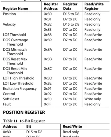
Table 10. Register Map
Register Name Register Address Register Data Read/Write Register
Position 0x80 D15 to D8 Read only
0x81 D7 to D0 Read only
Velocity 0x82 D15 to D8 Read only
0x83 D7 to D0 Read only
LOS Threshold 0x88 D7 to D0 Read/write
DOS Overrange Threshold 0x89 D7 to D0 Read/write DOS Mismatch Threshold 0x8A D7 to D0 Read/write
DOS Reset Max Threshold
0x8B D7 to D0 Read/write
DOS Reset Min Threshold
0x8C D7 to D0 Read/write
LOT High Threshold 0x8D D7 to D0 Read/write
LOT Low Threshold 0x8E D7 to D0 Read/write
Excitation Frequency 0x91 D7 to D0 Read/write
Control 0x92 D7 to D0 Read/write
Soft Reset 0xF0 D7 to D0 Write only
Fault 0xFF D7 to D0 Read only
POSITION REGISTER
Table 11. 16-Bit Register
Address Bit Read/Write
0x80 D15 to D8 Read only
0x81 D7 to D0 Read only
The position register contains a digital representation of the angular position of the resolver input signals. The values are stored in 16-bit binary format. The value in the position register is updated following a falling edge on the SAMPLE input. Note that with hysteresis enabled (see the Control Register section), at lower resolutions, the LSBs of the 16-bit digital output are set to zero. For example, at 10-bit resolution, Data Bit D15 to Data Bit D6 provide valid data; D5 to D0 are set to zero. With hysteresis dis-abled, the value stored in the position register is 16 bits regardless of resolution. At lower resolutions, the LSBs of the 16-bit digital output can be ignored. For example, at 10-bit resolution, Data Bit D15 to Data Bit D6 provide valid data; D5 to D0 can be ignored.
VELOCITY REGISTER
Table 12. 16-Bit Register
Address Bit Read/Write
0x82 D15 to D8 Read only
0x83 D7 to D0 Read only
The velocity register contains a digital representation of the angular velocity of the resolver input signals. The value in the velocity register is updated following a falling edge on the sample input. The values are stored in 16-bit, twos complement format. The
maximum velocity that the AD2S1210 can track for each resolution is specified in Table 1. For example, the maximum tracking rate of the AD2S1210 at 16 bits resolution, with an 8.192 MHz input clock, is ±125 rps. A velocity of +125 rps results in 0x7FFF being stored in the velocity register; a velocity of −125 rps results in 0x8000 being stored in the velocity register. The value stored in the velocity register is 16 bits regardless of resolution. At lower resolutions, the LSBs of the 16-bit digital output should be ignored. For example, at 10-bit resolution, Data Bit D15 to Data Bit D6 provide valid data; D5 to D0 should be ignored. The maximum tracking rate of the AD2S1210 at 10-bit resolution with an 8.192 MHz input clock is ±2500 rps. A velocity of +2500 rps results in 0x1FF being stored in Bit D15 to Bit D6 of the velocity register; a velocity of −2500 rps results in 0x3FF being stored in Bit D15 to Bit D6 of the velocity register. In this 10-bit example, the LSB size of the velocity output is 4.88 rps.
LOS THRESHOLD REGISTER
Table 13. 8-Bit Register
Address Bit Read/Write
0x88 D7 to D0 Read/write
The LOS threshold register determines the loss of signal threshold of the AD2S1210. The AD2S1210 allows the user to set the LOS threshold to a value between 0 V and 4.82 V. The resolution of the LOS threshold is seven bits, that is, 38 mV. Note that the MSB, D7, should be set to 0. The default value of the LOS threshold on power-up is 2.2 V.
DOS OVERRANGE THRESHOLD REGISTER
Table 14. 8-Bit Register
Address Bit Read/Write
0x89 D7 to D0 Read/write
The DOS overrange threshold register determines the degradation of signal threshold of the AD2S1210. The AD2S1210 allows the user to set the DOS overrange threshold to a value between 0 V and 4.82 V. The resolution of the DOS overrange threshold is seven bits, that is, 38 mV. Note that the MSB, D7, should be set to 0. The default value of the DOS overrange threshold on power-up is 4.1 V.
DOS MISMATCH THRESHOLD REGISTER
Table 15. 8-Bit Register
Address Bit Read/Write
0x8A D7 to D0 Read/write
The DOS mismatch threshold register determines the signal mismatch threshold of the AD2S1210. The AD2S1210 allows the user to set the DOS mismatch threshold to a value between 0 V and 4.82 V. The resolution of the DOS mismatch threshold is seven bits, that is, 38 mV. Note that the MSB, D7, should be set to 0.The default value of the DOS mismatch threshold on power-up is 380 mV.
THRESHOLD REGISTERS
Table 16. 8-Bit Registers
Address Bit Read/Write
0x8B D7 to D0 Read/write
0x8C D7 to D0 Read/write
The AD2S1210 continuously stores the minimum and maximum magnitude of the monitor signal in internal registers. The differ-ence between the minimum and maximum is calculated to determine if a DOS mismatch has occurred. The initial values for the minimum and maximum internal registers must be defined by the user. When the fault register is cleared, the registers that store the maximum and minimum amplitudes of the monitor signal are reset to the values stored in the DOS reset maximum and minimum threshold registers. The resolution of the DOS reset maximum and minimum thresholds is seven bits each, that is, 38 mV. Note that the MSB, D7, should be set to 0.To ensure correct operation, it is recommended that the DOS reset minimum threshold register be set to at least 1 LSB less than the DOS overrange threshold, and the DOS reset maximum threshold register be set to at least 1 LSB greater than the LOS threshold register. The default value of the DOS reset minimum threshold register and the DOS reset maximum threshold register are 3.99 V and 2.28 V, respectively.
LOT HIGH THRESHOLD REGISTER
Table 17. 8-Bit Register
Address Bit Read/Write
0x8D D7 to D0 Read/write
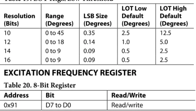
The LOT high threshold register determines the loss of position tracking threshold for the AD2S1210. The LOT high threshold is a 7-bit word. Note that the MSB, D7, should be set to 0. The range of the LOT high threshold, the LSB size, and the default value of the LOT high threshold on power-up are dependent on the resolution setting of the AD2S1210, and are outlined in Table 19.
LOT LOW THRESHOLD REGISTER
Table 18. 8-Bit Register
Address Bit Read/Write
0x8E D7 to D0 Read/write
The LOT low threshold register determines the level of hysteresis on the loss of position tracking fault detection. Loss of tracking (LOT) occurs when the internal error signal of the AD2S1210 exceeds the LOT high threshold. LOT has hysteresis and is not cleared until the internal error signal is less than the value defined in the LOT low threshold register. The LOT low threshold is a 7-bit word. Note that the MSB, D7, should be set to 0. The range
Resolution (Bits) Range (Degrees) LSB Size (Degrees) LOT Low Default (Degrees) LOT High Default (Degrees) 10 0 to 45 0.35 2.5 12.5 12 0 to 18 0.14 1.0 5.0 14 0 to 9 0.09 0.5 2.5 16 0 to 9 0.09 0.5 2.5
EXCITATION FREQUENCY REGISTER
Table 20. 8-Bit Register
Address Bit Read/Write
0x91 D7 to D0 Read/write
The excitation frequency register determines the frequency of the excitation outputs of the AD2S1210. A 7-bit frequency control word is written to the register to set the excitation frequency. Note that the MSB, D7, should be set to 0.
(
)
CLKIN f Frequency Excitation FCW 15 2 × = (9)where FCW is the frequency control word and fCLKIN is the clock
frequency of the AD2S1210. The specified range of the excitation frequency is from 2 kHz to 20 kHz and can be set in increments of 250 Hz. To ensure that the AD2S1210 is operated within the specified frequency range, the frequency control word should be a value between 0x4 and 0x50.
For example, if the user requires an excitation frequency of 5 kHz and has an 8.192 MHz clock frequency, the code that needs to be programmed is given by
(
)
14 MHz 192 . 8 2 kHz 5 15 = × = FCW (hexadecimal)The default excitation frequency of the AD2S1210 on power-up is 10 kHz.
CONTROL REGISTER
Table 21. 8-Bit Register
Address Bit Read/Write
0x92 D7 to D0 Read/write
The control register is an 8-bit register that sets the AD2S1210 control modes. The default value of the control register on power-up is 0x7E.
Table 22. Control Register Bit Descriptions
Bit Description
D7 Address/data bit
D6 Reserved; set to 1
D5 Phase lock range
Address/Data Bit
The MSB of each 8-bit word written to the AD2S1210 indicates whether the 8-bit word is a register address or data. The MSB (D7) of each register address defined on the AD2S1210 is high. The MSB of each data word written to the AD2S1210 is low. Note that when a data word is written to the AD2S1210, the MSB is internally reconfigured as a parity bit. When reading data from any of the read/write registers (see Table 10), the parity of Bit D6 to Bit D0 is recalculated and compared to the previously stored parity bit. The MSB of the 8-bit output is used to indicate whether a configuration error has occurred. If the MSB is returned high, this indicates that the data read back from the device does not match the configuration data written to the device in the previous write cycle.
Phase Lock Range
The phase lock range allows the AD2S1210 to compensate for phase errors between the excitation frequency and the sine/cosine inputs. The recommended mode of operation is to use the default phase lock range of ±44°. If additional phase lock range is required, a range of 360° can be set. However, in this mode of operation, the AD2S1210 should be reset following a loss of signal error. Failure to do so may result in a 180° error in the angular output data.
Hysteresis
The AD2S1210 includes a hysteresis function, ±1 LSB, between the output of the position integrator and the input to the position register. When operating in a noisy environment, this can be used to prevent flicker on the LSB. On the AD2S1210, the maximum tracking rate is defined by the bandwidth. Each resolution setting is internally configured with a different bandwidth, as outlined in Table 1. The maximum tracking rate and the bandwidth are inversely proportional to the resolution, that is, the maximum tracking rate increases as the resolution is decreased. The option of disabling the hysteresis allows the user to oversample the position output and to achieve a higher resolution output within the specified bandwidths through external averaging. The hysteresis function can be enabled or disabled through setting Bit D4 in the control register. Hysteresis is enabled by default on power-up.
Set Encoder Resolution
The resolution of the encoder outputs of the AD2S1210 can be set to the same resolution as the digital output or it can also be set to a lower resolution. For example, when the resolution of the AD2S1210 position outputs is set to 16 bits, the resolution of the encoder outputs may be set to 14, 12, or 10 bits. This allows the user to take advantage of the lower bandwidth and improved performance of the 16-bit resolution setting without requiring external divide down of the A-quad-B encoder outputs. The default resolution of the encoder outputs on power-up is 16 bits. Refer to the Incremental Encoder Outputs section.
Table 23. Encoder Resolution Settings
EnRES0 EnRES1 Resolution (Bits)
0 0 10 0 1 12 1 0 14 1 1 16
Set Resolution
In normal mode, the resolution of the digital output is selected using the RES0 and RES1 input pins (see Table 9). In configuration mode, the resolution is selected by setting the RES0 and RES1 bits in the control register. When switching between normal mode and configuration mode, it is the responsibility of the user to ensure that the resolution set in the control register matches the resolution set by the RES0 and RES1 input pins. The default resolu-tion of the digital output on power-up is 12 bits.
SOFTWARE RESET REGISTER
Table 24. 8-Bit Register
Address Bit Read/Write
0xF0 D7 to D0 Write only
Addressing the software reset register, that is writing the 8-bit address, 0xF0, of the software reset register to the AD2S1210 while in configuration mode, allows the user to initiate a soft-ware reset of the AD2S1210. The softsoft-ware reset reinitializes the excitation frequency outputs and the internal Type II tracking loop. The data stored in the configuration registers is not overwritten by a software reset. However, it should be noted that the data in the fault register is reset. In an application that uses two or more resolver-to-digital converters, which are both driven from the same clock source, the software reset can be used to synchronize the phase of the excitation frequencies across the converters.
FAULT REGISTER
Table 25. 8-Bit Register
Address Bit Read/Write
0xFF D7 to D0 Read only
The AD2S1210 has the ability to detect eight separate fault condi-tions. When a fault occurs, the DOS and/or the LOT output pins are taken low. By reading the fault register, the user can determine the cause of the triggering of the fault detection output pins. Note that the fault register bits are active high, that is, the fault bits are taken high to indicate that a fault has occurred. Table 26. Fault Register Bit Descriptions
Bit Description
D7 Sine/cosine inputs clipped
D6 Sine/cosine inputs below LOS threshold
D5 Sine/cosine inputs exceed DOS overrange threshold
D4 Sine/cosine inputs exceed DOS mismatch threshold
D3 Tracking error exceeds LOT threshold
D2 Velocity exceeds maximum tracking rate
D1 Phase error exceeds phase lock range D0 Configuration parity error
DIGITAL INTERFACE
The angular position and angular velocity are represented by binary data and can be extracted either via a 16-bit parallel interface or via a 4-wire serial interface that operates at clock rates of up to 25 MHz. The AD2S1210 programmable functions are controlled using a set of on-chip registers. Data is written to these registers using either the serial or the