CH7025/CH7026
Advance InformationChrontel
CH7025/CH7026 TV/VGA Encoder
F
EATURES
G
ENERAL
D
ESCRIPTION
• Support multiple output formats. Such as SDTV format
(NTSC and PAL), HDTV format for 480p,576p,720p and 1080i, analog RGB output for VGA. Sync signals can be
provided in separated or composite manner
(Programmable composite sync generation).
• Three on-chip 10-bit high speed DACs providing flexible
output capabilities. Such as single, double or triple CVBS outputs, YPbPr output, RGB output and simultaneous CVBS and S-video outputs.
• Internal embedded 16Mbits SDRAM is used as frame
buffer. Supporting for frame rate conversion. 90/180/270 degree image rotation and vertical or horizontal flip functions are supported.
• Programmable 24-bit/18-bit/16-bit/15-bit/12-bit/8-bit
digital input interface supports various RGB (RGB888, RGB666, RGB565 and etc), YCbCr (4:4:4 YCbCr, ITU656) and 2x or 3x multiplexed input. CPU/Memory interface are supported.
• Support for flexible input resolution is up to 800x800 and
1024x680. 320x240, 640x480, 960x720 are support.
• Bypass mode is supported.
• Flexible up and down scaling engine is embedded
including de-flickering capability. Text enhancement is supported.
• Pixel by pixel brightness, contrast, hue and saturation
adjustment for each kind of output are supported. For RGB output, only brightness and contrast adjustment are supported.
• Pixel by pixel horizontal position adjustment and line by
line vertical position adjustment are supported.
• Fully programmable through serial port. IO and SPC/SPD
voltage supported is from 1.2V to 3.3V.
• TV/Monitor connection detect capability.
• Programmable power management. DAC can be switched
off based on detection result (Driver support is required).
• Flexible pixel clock frequency from graphics controller is
supported (2.3MHz –120MHz). Flexible input clock from crystal or oscillator is supported (2.3MHz – 64MHz).
• MacrovisionTM 7.1.L1 for SDTV is supported in CH7025
(CH7026 is Non-Macrovision part.). MacrovisionTM copy protection support for progressive scan TV (480p, 576p CH7025 only).
• CGMS-Asupport for SDTV and HDTV (CH7025 only).
• Offered in BGA or QFP package.
The CH7025/CH7026 is a device targeting handheld and similar consumer systems which accept digital input signal. CH7025/CH7026 encodes and transmits data through 10-bit DACs. The device is able to
encode the video signals and generate
synchronization signals SDTV format for NTSC and
PAL standards and HDTV format for
480p,576p,720p and 1080i. Analog RGB output and composite SYNC signal are also supported. The device accepts different data formats including RGB and YCbCr (e.g. RGB565, RGB666, RGB888, ITU656 like YCbCr, etc.).Both interlaced and non-interlaced input data formats are supported. 16Mbit SDRAM is embedded in package. Frame rate conversion, Image rotation, zooming and scaling, are supported.
Note: the above feature list is subject to change without notice. Please contact Chrontel for more information and current updates.
CHRONTEL
CH7025/CH7026
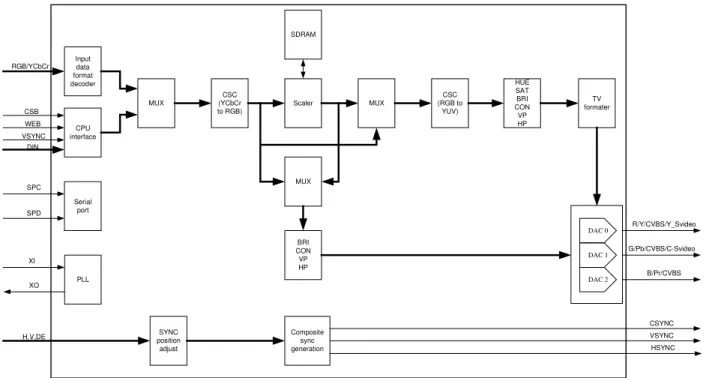
Input data format decoder RGB/YCbCr CPU interface CSB WEB VSYNC DIN MUX CSC (YCbCr to RGB) Scaler SDRAM HUE SAT BRI CON VP HP TV formater MUX BRI CON VP HP DAC 0 DAC 2 DAC 1 R/Y/CVBS/Y_Svideo G/Pb/CVBS/C-Svideo B/Pr/CVBS Serial port SPC SPD PLL XI XO SYNC position adjustH,V,DE Composite sync generation CSYNC VSYNC HSYNC CSC (RGB to YUV) MUX
CHRONTEL
CH7025/CH7026
Table of Contents
F
EATURES... 1
G
ENERALD
ESCRIPTION... 1
1.0
P
IN-
OUT... 6
1.1 Package Diagram ...6 1.2 Pin Description ...72.0
F
UNCTIONALD
ESCRIPTION... 11
2.1 Input Interface ...11 2.1.1 Overview...112.1.2 Input Clock and Data Timing Diagram...11
2.1.3 Input Data Voltage...12
2.1.4 Input Data Format ...12
2.2 Chip Output ...14
2.2.1 TV Output ...14
2.2.2 VGA Output...15
2.2.3 Video DAC Output ...15
2.2.4 DAC Single/Double Termination ...15
2.2.5 Video DAC Connection Detect ...15
2.2.6 Picture Enhancement ...15
2.2.7 Color Sub-carrier Generation...15
2.2.8 ITU-R BT.470 Compliance ...16
2.3 Testing Functions and Power Down Mode ...16
2.3.1 Test Pattern Select ...16
2.3.2 SDRAM Power Down ...16
2.4 Serial Port...16
2.4.1 Introduction...16
2.4.2 Electrical Characteristics of the Serial Port ...17
2.4.3 Transfer Protocol ...17
2.4.4 Chrontel Encoder Write Cycle Protocol (R/W* = 0)...18
2.4.5 Chrontel Encoder Read Cycle Protocol (R/W* = 1)...19
3.0
E
LECTRICALS
PECIFICATIONS... 21
3.1 Absolute Maximum Ratings ...21
3.2 Recommended Operating Conditions ...21
3.3 Electrical Characteristics ...22
3.4 Digital Inputs / Outputs...22
3.5 AC Specifications ...23
4.0
P
ACKAGED
IMENSIONS... 24
CHRONTEL
CH7025/CH7026
FIGURES AND TABLES
List of Figures
Figure 1: CH7025/CH7026 Block Diagram ...2
Figure 2: BGA Package (Top View) ...6
Figure 3: 80 Pin LQFP Package ...7
Figure 4: Clock and Data Input Timing in 3x Multiplexed Mode ...11
Figure 5: SDR and DDR Input Data Formats ...11
Figure 6: Horizontal Input Timing...12
Figure 7: Vertical Input Timing...12
Figure 8: CPU/MEMORY Interface Timing ...12
Figure 9: The Connection of the Serial Port Interface ...17
Figure 10: Acknowledge Protocol ...19
Figure 11:Single-step Write Cycles (2 cycles) ...19
Figure 12:Auto-Increment Write Cycle ...19
Figure 13: Single-step Read Cycles (2 cycles) ...20
Figure 14:Auto-increment Read Cycles...20
Figure 15: 80 Pin TFBGA Package ...24
Figure 16: 80 Pin LQFP Package ...25
List of Tables
Table 1: Pin Name Description (BGA Package) ...7Table 2: Pin Name Descriptions (LQFP80 Package)...9
Table 3: Input Data Format...13
Table 4: Supported SDTV Standards...14
Table 5: Supported EDTV/HDTV Standards ...14
Table 6: Composite Sync Type...15
Table 7: Video DAC Configurations for CH7025/CH7026 ...15
CHRONTEL
CH7025/CH7026
1.0 P
IN
-
OUT
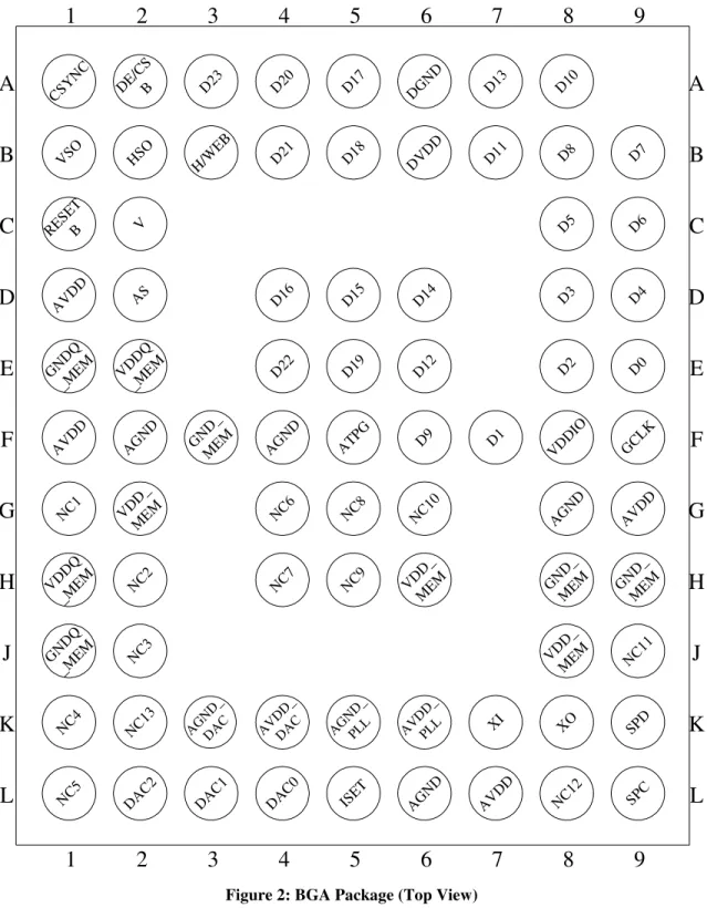
1.1 Package Diagram
NC 8 VD D_ MEM NC 11 AV DD NC 2 GN D_ MEM VD D_ MEM N C6 GC LK AG ND AV DD D9 D0 GN DQ _M EM AG ND NC 10 D1 VD DIO D2 AS AV DD D3 D4 RES ET B D15 NC 7 VD D_ MEM GN D_ MEM VD DQ _M EM NC 1 D12 D23 DV DD D5 D6 V D20 D17 D11 D8 HSO VSO H/WEB D21 D18 D7 D13 D10 D16 DE/ CS B CSY NC NC 3 GN DQ _M EMA
B
C
D
E
F
G
H
J
VD DQ _M EM ATP G GN D_ MEMA
B
C
D
E
F
G
H
J
1
2
3
4
5
6
7
8
9
D19 D22 NC 9 D14 AG ND DG ND AV DD _ PLL X I SPC NC 13 DA C0 DA C1 AV DD _ DA C AG ND AV DD NC 12 SPD NC 4 AG ND _ DA C DA C2 NC 5K
L
XO1
2
3
4
5
6
7
8
9
K
L
ISET AG ND _ PLLCHRONTEL
CH7025/CH7026
1 2 3 4 5 6 7 8 9 10 11 12 13 14 15 16 17 18 19 20 2 1 2 2 2 3 2 4 2 5 2 6 2 7 2 8Chrontel
CH7025/CH7026
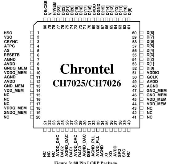
2 9 3 0 3 1 3 2 3 3 3 4 3 5 3 6 3 7 3 8 3 9 4 0 HSO D [1 0 ] D[8] D[7] D[6] D [9 ] D [1 2 ] D [1 9 ] D [1 7 ] D [1 6 ] D [1 5 ] D [1 4 ] D [1 3 ] D [1 1 ] D [1 8 ] D [2 0 ] D [2 2 ] D V D D D E /C S B V H/W E B D [2 3 ] D [2 1 ] D G N D VSO CSYNC D[3] D[5] D[4] D[2] VDDIO GCLK GND_MEM VDD_MEM NC NC NC AGND AVDD D[0] D[1] GND_MEM VDD_MEM A V D D _ D A C D A C 2 A G N D _ D A C D A C 1 A V D D _ D A C D A C 0 A G N D _ D A C IS E T A G N D _ P L L A V D D _ P L L A G N D A V D D X I X O S P C S P D N C N C N C N C ATPG AS RESETB AGND AVDD GNDQ_MEM VDDQ_MEM NC NC NC GNDQ_MEM VDDQ_MEM AGND AVDD GND_MEM VDD_MEM NC 8 0 7 9 7 8 7 7 7 6 7 5 74 7 3 7 2 7 1 7 0 6 9 6 8 6 7 6 6 6 5 6 1 6 2 6 3 6 4 60 41 42 43 44 45 46 47 48 49 50 51 52 53 54 55 56 57 58 59Figure 3: 80 Pin LQFP Package
1.2 Pin Description
Table 1: Pin Name Description (BGA Package)
Pin # Type Symbol Description
A3, E4, B4, A4, E5, B5, A5, D4, D5, D6, A7, E6, B7, A8, F6, B8, B9, C9, C8, D9, D8, E8, F7, E9
In D[23:0] [1] Data[0] through Data[23] Inputs
These pins accept the 24 data inputs from a digital video port of a graphics controller. The swing is defined by VDDIO.
C2 In/Out V Vertical Sync Input / Output
When the SYO control bit is low, this pin accepts a vertical sync input for use with the input data.
When the SYO control bit is high, the device will output a vertical sync pulse. The output is driven from the VDDIO supply.
B3 In/Out H/WEB Horizontal Sync Input / Output
When the SYO control bit is low, this pin accepts a horizontal sync input for use with the input data.
When the SYO control bit is high, the device will output a horizontal sync pulse. The output is driven from the VDDIO supply.
CHRONTEL
CH7025/CH7026
A2 In DE/CSB Data Input Indicator
When the pin is high, the input data is active. When the pin is low, the input data is blanking. It is also the CSB signal of CPU/MEMORY interface.
D2 In AS Serial Port Device Address Select (7-bit address + R/W bit)
0: 76h 1: 75h
F5 In ATPG ATPG Enable (Internally pull-low)
This pin should be left open or pulled low with a 10 kΩ
resistor in the application. This pin configures the pre-condition for scan chain and boundary scan test when high. Otherwise it should be pulled low. Voltage level is 0 to 3.3V.
C1 In RESETB Active low reset.
When RESETB is low, the device is held in the hardware reset condition. When RESETB is high, reset is controlled through the serial port.
K9 In/Out SPD Serial Port Data Input / Output (open drain)
This pin functions as the bi-directional data pin of the serial port. External pull-up resistor is required.
L9 In SPC Serial Port Clock Input (open drain)
This pin functions as the clock pin of the serial port. External pull-up resistor is required.
L4 Out DAC0 CVBS, S-video, YPbPr or Analog RGB output
Full swing is up to 1.3 V.
L3 Out DAC1 CVBS, S-video, YPbPr or Analog RGB output
Full swing is up to 1.3 V.
L2 Out DAC2 CVBS, S-video, YPbPr or Analog RGB output
Full swing is up to 1.3 V.
L5 In ISET Current Set
This pin sets the DAC current. A 1.2 kΩ, 1% tolerance resistor should be connected between this pin and AGND_DAC using short and wide trace.
K7 In XI Crystal Input / External Input
For some situation of the slave mode, a parallel resonance crystal (± 20 ppm) should be attached between this pin and
XO. However, an external 3.3V CMOS compatible clock can drive the XI input.
K8 Out XO Crystal Output
For some situation of the slave mode, a parallel resonance crystal (± 20 ppm) should be attached between this pin and
XI. However, if an external CMOS clock is attached to XI, XO should be left open.
F9 In GCLK Graphics Controller Clock Input
B1 Out VSO Vertical sync signal output
B2 Out HSO Horizontal sync signal output
A1 Out CSYNC Composite sync output
F8 Power VDDIO IO supply voltage(1.2-3.3V)
B6 Power DVDD Digital supply voltage (1.8V)
D1, F1, L7, G9 Power AVDD Analog supply voltage (2.5 – 3.3V)
K6 Power AVDD_PLL PLL supply voltage (1.8V)
K4 Power AVDD_DAC DAC power supply (2.5 – 3.3V)
E2, H1 Power VDDQ_MEM SDRAM output buffer supply voltage (2.5V)
CHRONTEL
CH7025/CH7026
A6 Power DGND Digital supply ground
F4, F2, L6, G8 Power AGND Analog supply ground
K5 Power AGND_PLL PLL supply ground
K3 Power AGND_DAC DAC supply ground
E1, J1 Power GNDQ_MEM SDRAM output buffer supply ground
F3, H9, H8 Power GND_MEM SDRAM device supply ground
Notes:
1. All the unused Data input pins should be pulled low with 10 kΩresistors or shorted to Ground directly.
Table 2: Pin Name Descriptions (LQFP80 Package)
Pin # Type Symbol Description
52 - 67 70 - 77
In D[23:0] [1] Data[0] through Data[23] Inputs
These pins accept the 24 data inputs from a digital video port of a graphics controller. The swing is defined by VDDIO.
79 In/Out V Vertical Sync Input / Output
When the SYO control bit is low, this pin accepts a vertical sync input for use with the input data.
When the SYO control bit is high, the device will output a vertical sync pulse. The output is driven from the VDDIO supply.
78 In/Out H/WEB Horizontal Sync Input / Output
When the SYO control bit is low, this pin accepts a horizontal sync input for use with the input data.
When the SYO control bit is high, the device will output a horizontal sync pulse. The output is driven from the VDDIO supply.
It is also the WEB signal of CPU/MEMORY interface.
80 In DE/CSB Data Input Indicator
When the pin is high, the input data is active. When the pin is low, the input data is blanking. CSB signal input of CPU/MEMORY interface.
5 In AS Serial Port Device Address Select (7-bit address + R/W bit)
0: 76h 1: 75h
4 In ATPG ATPG Enable (Internally pull-low)
This pin should be left open or pulled low with a 10 kΩ resistor in the application. This pin configures the pre-condition for scan chain and boundary scan test when high. Otherwise it should be pulled low. Voltage level is 0 to 3.3V.
6 In RESETB Reset * Input
When this pin is low, the device is held in the power-on reset condition. When this pin is high, reset is controlled through the serial port.
38 In/Out SPD Serial Port Data Input / Output (open drain)
This pin functions as the bi-directional data pin of the serial port. External pull-up resistor is required.
39 In SPC Serial Port Clock Input (open drain)
This pin functions as the clock pin of the serial port. External pull-up resistor is required.
29 Out DAC0 CVBS, S-video, YPbPr or Analog RGB output
Full swing is up to 1.3 V
27 Out DAC1 CVBS, S-video, YPbPr or Analog RGB output
Full swing is up to 1.3 V
25 Out DAC2 CVBS, S-video, YPbPr or Analog RGB output
CHRONTEL
CH7025/CH7026
31 In ISET Current Set
This pin sets the DAC current. A 1.2 kΩ, 1% tolerance resistor should be connected between this pin and AGND_DAC using short and wide trace.
35 In XI Crystal Input / External Input
For some situation of the slave mode, a parallel resonance crystal (± 20
ppm) should be attached between this pin and XO. However, an external 3.3V CMOS compatible clock can drive the XI input.
36 Out XO Crystal Output
For some situation of the slave mode, a parallel resonance crystal (± 20
ppm) should be attached between this pin and XI. However, if an external CMOS clock is attached to XI, XO should be left open.
50 In GCLK Graphics Controller Clock Input
2 Out VSO Vertical sync signal output,
The amplitude of this pin is from 0 to AVDD
1 Out HSO Horizontal sync signal output,
The amplitude of this pin is from 0 to AVDD
3 Out CSYNC Composite sync output,
The amplitude of this pin is from 0 to AVDD
51 Power VDDIO IO supply voltage(1.2-3.3V)
69 Power DVDD Digital supply voltage (1.8V)
8, 12 37, 49
Power AVDD Analog supply voltage (2.5 – 3.3V)
33 Power AVDD_PLL PLL supply voltage (1.8V)
24, 28 Power AVDD_DAC DAC power supply (2.5 – 3.3V)
10, 18 Power VDDQ_MEM SDRAM output buffer supply voltage (2.5V)
14, 44 45
Power VDD_MEM SDRAM device supply voltage (2.5V)
68 Power DGND Digital supply ground
7, 11, 34 48
Power AGND Analog supply ground
32 Power AGND_PLL PLL supply ground
26, 30 Power AGND_DAC DAC supply ground
9, 19 Power GNDQ_MEM SDRAM output buffer supply ground
13,46, 47 Power GND_MEM SDRAM device supply ground
Notes:
CHRONTEL
CH7025/CH7026
2.0 F
UNCTIONAL
D
ESCRIPTION
2.1 Input Interface
2.1.1 Overview
Five distinct methods of transferring data to the CH7025/CH7026 are described below. 1. Unitary data, clock input at 1X the pixel rate (SDR mode)
2. Multiplexed data, clock input at 1X of pixel rate (DDR mode) 3. Multiplexed data, clock input at 2X of pixel rate
4. Multiplexed data, clock input at 3X of pixel rate 5. 8/16/24 bit CPU/MEMORY interface
For the multiplexed data, clock at 1X pixel rate, the data applied to the CH7025/CH7026 is latched with both edges of the clock (also referred to as dual edge transfer mode or DDR). For the multiplexed data, clock at 2X or 3X pixel rate the data applied to the CH7025/CH7026 is latched with one edge of the clock (also known as single edge transfer mode or SDR). For the unitary data, clock at 1X pixel rate, the data applied to the CH7025/CH7026 is latched with one edge of the clock .The polarity of the pixel clock can be reversed through serial port control. Hsync and Vsync can be input individually or embedded into data signal such as BT656 input format.
2.1.2 Input Clock and Data Timing Diagram
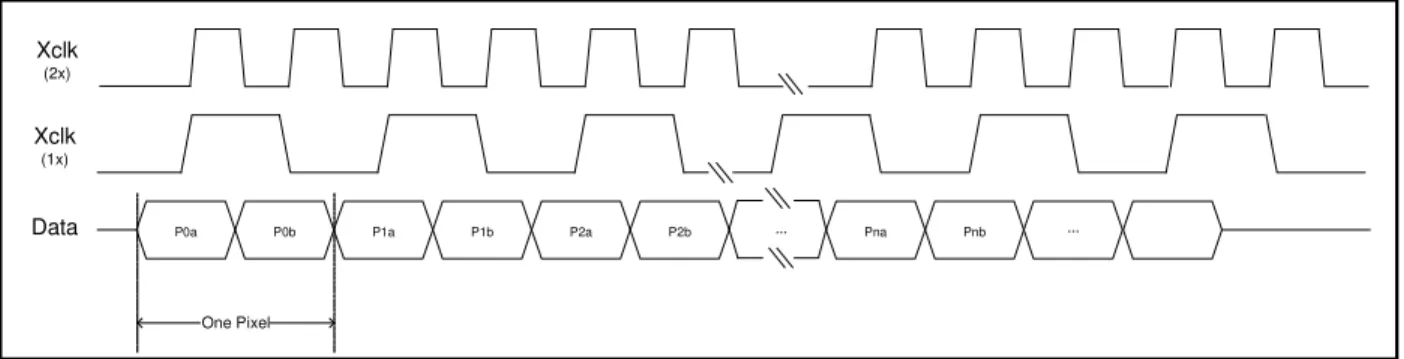
Figure 4 to Figure 8 below shows the timing diagram for input data and clocks. The timing requirements are given in later section. Pna Pnb Pnc … P1a P1b P1c P2a P2b P2c Data Xclk (3x) P0c P0b P0a … One Pixel
Figure 4: Clock and Data Input Timing in 3x Multiplexed Mode
Data Xclk (1x) One Pixel P1b P2a P2b P1a P0b P0a … Pna Pnb … Xclk (2x)
Figure 5: SDR and DDR Input Data Formats
(Note: In Figure 5, the first XCLK waveform represents the input clock for single edge transfer (SDR) methods. The second XCLK waveform represents the input clock for the dual edge transfer (DDR) method.)
CHRONTEL
CH7025/CH7026
Hsync Data DE Xclk (1x) HW HT HA HOFigure 6: Horizontal Input Timing
Vsync Line Hsync DE VW VT VA VO
Figure 7: Vertical Input Timing
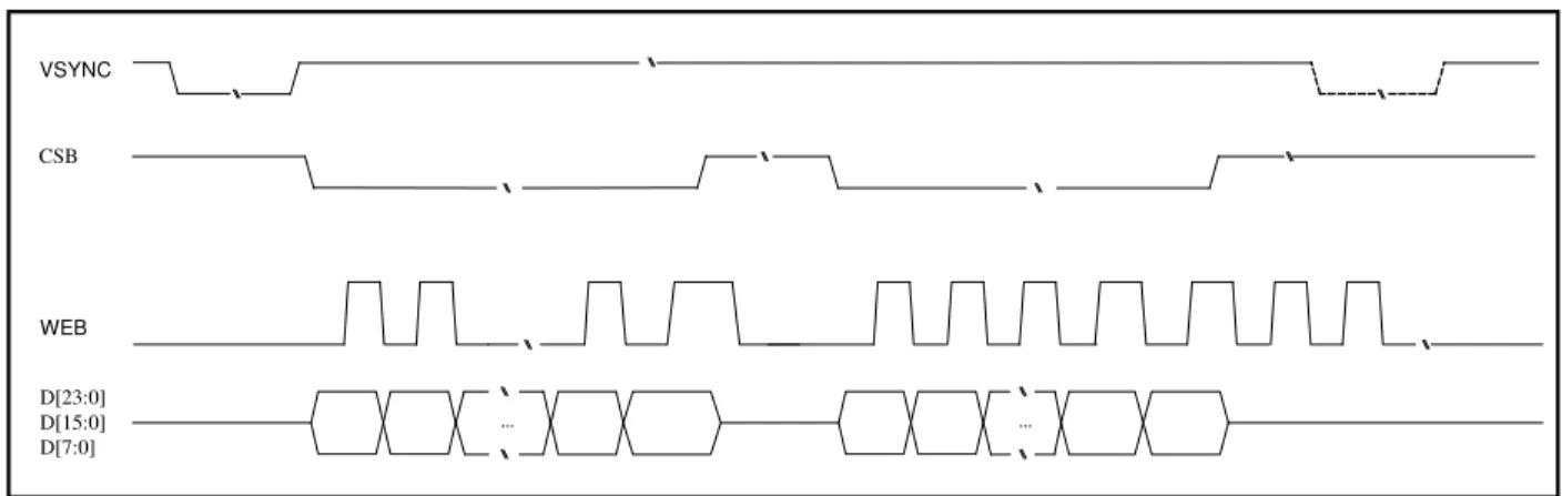
WEB … VSYNC CSB … D[23:0] D[15:0] D[7:0]
Figure 8: CPU/MEMORY Interface Timing
(Note: VSYNC pulse of CPU/MEMORY interface is not necessary for each input frame, it is required to appear at least one time at any input frame blank period.)
2.1.3 Input Data Voltage
The voltage level of input pins D[23:0], H/WEB, V, DE/CSB are from 0 to VDDIO. These pins support two input mode, one is CMOS mode, the other is pseudo differential mode. The default is CMOS mode with CMOS level on these pins. When control bit DIFFEN is high, the input is pseudo differential mode that uses a reference voltage (VREF) to compare with input voltage and decide input logic value. The VREF value can be 80%, 70%, 60% and 50% of VDDIO value, referring to VRTM[1:0]. The pseudo differential mode can accept the wide range of the input voltage level from 1.2v to 3.3v, while the CMOS mode can accept 1.8v to 3.3v input voltage.
2.1.4 Input Data Format
CHRONTEL
CH7025/CH7026
Table 3: Input Data FormatMULTI IDF D[23:16] D[15:8] D[7:0] 0 R[7:0] G[7:0] B[7:0] 1 2'b00,R[5:0] 2'b00,G[5:0] 2'b00,B[5:0] 2 3'b000,R[4:0] 2'b00,G[5:0] 3'b000,B[4:0] 3 3'b000,R[4:0] 3'b000,G[4:0] 3'b000,B[4:0] 4 R[7:3],G[7:5] R[2:0],G[1],G[4:2], B[7] B[6:3],G[0],B[2:0] 5 8'h00 Y[7:0] C[7:0] 6 4'h0, Y[9:6] Y[5:0],C[9:8] C[7:0] 7 Y[7:0] Cb[7:0] Cr[7:0]
8 Reserved Reserved Reserved
9 6'h00, R[5:4] R[3:0],G[5:2] G[1:0],B[5:0] 10 8'h00 R[4:0],G[5:3] G[2:0],B[4:0] 0 11 8'h00 1'b0, R[4:0],G[4:3] G[2:0],B[4:0] PA 4’h0, R[7:4] R[3:0],G[7:4] PB 0 4’h0, G[3:0] B[7:0] PA 7’h00, R[5] R[4:0],G[5,3] PB 1 7’h00, G[2] G[1:0],B[5:0] PA R[4:0],G[5,3] PB 2 G[2:0],B[4:0] PA 1’b0,R[4:0],G[4,3] PB 3 G[2:0],B[4:0] PA 4’h0, R[7:4] R[3],G[7:5],R[2:0],G[1] PB 4 4’h0, G[4:2], B [7] B[6:3],G[0],B[2:0] PA Y[7:0] PB 5 C[7:0] PA 6’h00, Y[9:8] Y[7:0] PB 6 6’h00, C[9:8] C[7:0] PA 4’h0, Y[7:4] Y[3:0],Cb[7:4] 1 PB 7 4’h0, Cb[3:0] Cr[7:0] PA R[7:0] PB G[7:0] PC 0 B[7:0] PA Y[7:0] PB Cb[7:0] 2 PC 7 Cr[7:0] (PA,PB,PC represent the parts of one pixel data)
IDF[3:0] describes the major input data format that CH7025/CH7026 accepts. They are: IDF = 0: 888 RGB(standard order) input
IDF = 1: 666 RGB input IDF = 2: 565 RGB input IDF = 3: 555 RGB input
CHRONTEL
CH7025/CH7026
IDF = 5: 8-bit YCbCr4:2:2 inputIDF = 6: 10-bit YCbCr4:2:2 input IDF = 7: 8-bit YCbCr4:4:4 input IDF = 8: Reserved
IDF = 9: Consecutive aligned 666 RGB input IDF = 10: Consecutive aligned 565 RGB input IDF = 11: Consecutive aligned 555 RGB input
Table 3 above describes the 24-bit input data format under unitary mode. For multiplexed input, input data need to be de-multiplexed to unitary input first then this table can be applied. The Pixel Data bus represents a 12-bit or 8-bit multiplexed data stream, which contains either RGB or YCbCr formatted data. The input data rate is 2X the pixel rate, and each pair of Pn values (e.g.; PA and PB) contains a complete pixel (3X input has the similar feature). When the input is a YCbCr data stream the color-difference data will be transmitted at half the data rate of the luminance data, with the sequence being set as Cb, Y, Cr, Y, where Cb0,Y0,Cr0 refers to co-sited luminance and color-difference samples and the following Y1 byte refers to the next luminance sample, per ITU-R BT.656 standards (the clock frequency is dependent upon the current mode, and is not 27MHz as specified in ITU-R BT.656). In YCbCr 4:2:2 with embedded sync mode, the hardware can detect the connection error and correct it automatically.
2.2 Chip Output
2.2.1 TV Output
The CH7025/CH7026 supports the following output formats:
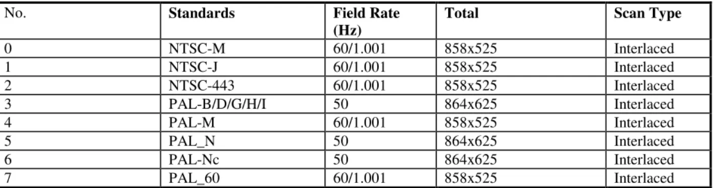
Table 4: Supported SDTV Standards
No. Standards Field Rate
(Hz)
Total Scan Type
0 NTSC-M 60/1.001 858x525 Interlaced 1 NTSC-J 60/1.001 858x525 Interlaced 2 NTSC-443 60/1.001 858x525 Interlaced 3 PAL-B/D/G/H/I 50 864x625 Interlaced 4 PAL-M 60/1.001 858x525 Interlaced 5 PAL_N 50 864x625 Interlaced 6 PAL-Nc 50 864x625 Interlaced 7 PAL_60 60/1.001 858x525 Interlaced
Table 5: Supported EDTV/HDTV Standards
Standards Field/Frame Rate (Hz) Total Active Clock (MHz) Scan Type
480/60p SMPTE293M EIA770.2A 60/1.001 858x525 or 1716x525 720x480 27 or 54 Progressive 576/50p ITU-R BT1358 50 864x625 or 1728x625 720x576 27 or 54 Progressive 720/60p SMPTE296M 60 or 60/1.001 1650x750 1280x720 74.25 or 74.176 Progressive 720/50p SMPTE296M 50 1980x750 1280x720 74.25 Progressive 1080/60i SMPTE274M 60 or 60/1.001 2200x1125 1920x1080 74.25 or 74.176 Interlaced
1080/50i SMPTE274M 50 2640x1125 1920x1080 74.25 Interlaced
1080/50i SMPTE295M 50 2376x1250 1920x1080 74.25 Interlaced
CVBS, S-video, YPbPr and analog RGB output are supported, when output analog RGB, composite sync output is available.
CHRONTEL
CH7025/CH7026
2.2.2 VGA OutputCH7025/CH7026 also supports analog RGB output through video DACs. Typically used resolution are 800x600, 856x480, 800x480 or 640x480. Vertical sync and horizontal sync signal are provided. Composite sync output is also supported. The type of composite sync can be programmed through register map.
Table 6: Composite Sync Type
CSSEL[2:0] Composite sync type
0 Vsync XOR Hsync
1 Vsync OR Hsync
2 Vsync AND Hsync
2.2.3 Video DAC Output
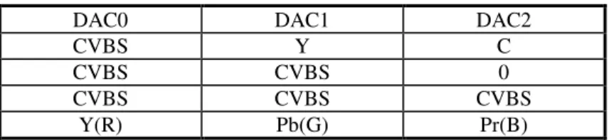
The DAC output is configured by the register bits VFMT[2:0]. DACS[1:0] bits are used to control the multiple output format i.e. dual or triple CVBS output, dual CVBS and S-Video output and etc. DACSP[2:0] bits are to swap the DAC output sequence such as CVBS, S-Video or S-Video, CVBS. Detailed information of these bits are described in register bits description section of this document. Table 7 below lists the DAC output configurations of the CH7025/CH7026:
Table 7: Video DAC Configurations for CH7025/CH7026
DAC0 DAC1 DAC2
CVBS Y C
CVBS CVBS 0
CVBS CVBS CVBS
Y(R) Pb(G) Pr(B)
2.2.4 DAC Single/Double Termination
The DAC output of CH7025/CH7026 can be single terminated or double terminated. Using single termination will save power consumption while double termination is likely to minimize the reflection from the cable. Refer to the description of register bit SEL_R.
2.2.5 Video DAC Connection Detect
CH7025/CH7026 can detect the Video DAC connection by setting register SPPSNS. It can detect which DAC is connected, short to ground or not connected.
2.2.6 Picture Enhancement
The CH7025/CH7026 has the capability of vertical and horizontal output picture position adjustment. It can automatically put the picture in the display center, and the vertical or horizontal position is also programmable through user input. And also it can provide brightness, contrast, hue, saturation adjustment and text enhancement functions. (For analog RGB output, only brightness and contrast adjustment are available).
CH7025/CH7026 also supports vertical or horizontal flip and rotation (0, 90, 180 and 270 degree) functions.
2.2.7 Color Sub-carrier Generation
CH7025/CH7026 has two ways to generate the color sub-carrier frequency. If the GCLK from the graphics controller has a steady center frequency and very small jitter, the sub-carrier can be derived from the GCLK. However, since even a ±0.01% sub-carrier frequency variation is enough to cause some TV to lose color lock,
CH7025/CH7026 has the ability to generate the sub-carrier frequency from the crystal when the GCLK from the graphics device cannot meet the requirement. In this case, the crystal has to be present.
CHRONTEL
CH7025/CH7026
In addition, CH7025/CH7026 has the capability to gen-lock the color sub-carrier with Vsync. Also, it has the ability to operate in a “stop dot crawl” mode for NTSC CVBS output when the first sub-carrier generation method is used.2.2.8 ITU-R BT.470 Compliance
The SDTV output of CH7025/CH7026 is mostly compliant with ITU-R BT.470 standard except for the items below.
• The frequencies of horizontal sync, vertical sync, and color sub-carrier depend on the quality of GCLK from
graphics controller and/or the off-chip crystal.
• It is assumed that gamma correction, if required, is performed in the graphics device.
• Pulse widths and rise/fall times for sync pulses, front/back porches, and equalizing pulses are designed to
approximate ITU-R BT.470 requirements. However, they may have a small variation depending on the actual input and output format.
• The actual bandwidths of the luminance and chrominance signals depend on the input resolution and the filter
selection.
2.3 Testing Functions and Power Down Mode
2.3.1 Test Pattern Select
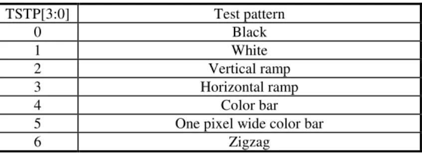
Setting TSTP[3:0] of 04h on the second page of register map can select different video patterns that go through datapath, according to the following table. TEST (bit5 of 04h on the second page) has to be 1 to enable test mode. TSYNC is to select which sync will be used internally generated sync or external input sync.
Table 8: Test Pattern Selection
TSTP[3:0] Test pattern 0 Black 1 White 2 Vertical ramp 3 Horizontal ramp 4 Color bar
5 One pixel wide color bar
6 Zigzag
2.3.2 SDRAM Power Down
SDRAM has two kinds of power down modes. One is power down mode, the other is deep power down mode. For power down mode, all data contents will be held in the bank. For deep power down mode, a command is required to issued. There is a bit called MEMPD in register map. It can be used to enable the deep power mode. During deep power mode, all the data in memory banks will be lost, and the SDRAM leakage current is less than 1 µA. A very important thing required to be noted here is that not all the SDRAM parts support either power down or deep power down mode. In these cases, even CH7025/CH7026 enters into power down, the leakage current is still large ( >100 µA ). In deep power down mode, the current consumption of SDRAM is less than 10 µA. (This leakage current is primarily derived from the SDRAM die. )
2.4 Serial Port
2.4.1 Introduction
The Chrontel CH7025/CH7026 contains a serial port interface, through which the control registers can be written to and read from. The serial interface consists of SPD (bidirectional serial port data) and SPC (serial port clock).
CHRONTEL
CH7025/CH7026
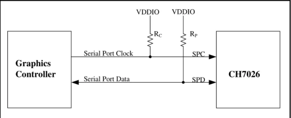
The serial port clock line (SPC) is input only and is driven by the output buffer of the graphics controller device, which is the clock master in the system. The serial port data line (SPD) is either input to or output from the encoder depending on the write or read status. The data on the line can be transferred up to 400 kbits/s. Figure 9 shows the connection of the serial port interface.Graphics Controller CH7026 SPD SPC Serial Port Clock
Serial Port Data
RP
RC
VDDIO VDDIO
Figure 9: The Connection of the Serial Port Interface
2.4.2 Electrical Characteristics of the Serial Port
The connections of the serial port interface is shown in Figure 9. A pull-up resistor (RP) must be connected to the
same voltage supply seen by the serial port interface pins. The serial port input voltage level is determined by VDDIO. A weak pull-up resister (RC) may be added to the clock line to ensure that it is pulled high when
the line is free.
Maximum and minimum values of pull-up resistor (RP)
The value of RP depends on the following parameters:
• Supply voltage • Line capacitance
• Number of devices connected (input current + leakage current = Iinput)
The supply voltage limits the minimum value of resistor RP due to the specified minimum sink current of 2mA at
VOLmax = 0.4 V for the output stages:
RP >= (VDD - 0.4) / 2 (where: RP is in kΩ)
The line capacitance is the total capacitance of wire, connections and pins. This capacitance limits the maximum value of RP due to the specified rise time. The equation for RP is shown below:
RP <= 103/C (where: RP is in kΩ and C, the total capacitance, is in pF)
The maximum HIGH level input current of each input/output connection has a specified maximum value of 10 µA. Due to the desired noise margin of 0.2VDD for the HIGH level, the input current limits the maximum value
of RP. The RP limit depends on VDD and is shown below:
RP <= (100 x VDD)/ Iinput (where: RP is in kΩ and Iinput is in µA)
2.4.3 Transfer Protocol
Both read and write cycles can be executed in “Single-step”, or “Auto-increment”. Auto-increment read/write allows you to establish the initial register location, then automatically increments the register address after each subsequent data access so that the next register address does not need to be resent through the SPC/SPD serial interface lines. When Auto-increment is set, the initial address is first sent to the encoder then data1 is sent, then data2, then data3, and so forth. Single-step read/write, is a simplified version of the Auto-increment read/write with a single set of data
CHRONTEL
CH7025/CH7026
instead of multiple data that is sent to or received from a specific register. The description of the transfer protocol is as follows:The transfer sequence is initiated when a high-to-low transition of SPD occurs while SPC is high; this is the “START” condition. Transitions of address and data bits can only occur while SPC is low.
The transfer sequence is terminated when a low-to-high transition of SPD occurs while SPC is high; this is the “STOP” condition.
Upon receiving the first START condition, the Chrontel encoder expects a Device Address Byte (DAB) from the master device. The DAB data format is shown below. Bits B[7:1] of the DAB is referred to as the serial port address. When the AS pin of the CH7025/CH7026 is pulled low, the Device Address Byte becomes ECh for serial port write and EDh for serial port read. When the AS pin of the CH7025/CH7026 is pulled high, the Device Address Byte becomes EAh for serial port write and EBh for serial port reads.
After the DAB is received, the Chrontel encoder expects a Register Address Byte (RAB) from the master.
The data format of the RAB is shown below.
CH7025/CH7026 Device Address Byte (DAB)
Bit7 Bit6 Bit5 Bit4 Bit3 Bit2 Bit1 Bit0
1 1 1 0 1 AS* AS R/W*
AS Address Select
For the CH7025/CH7026, the value of this bit is determined by the status of the AS pin. When the pin is strapped low, the value of AS = 0. When the pin is strapped high, the value of AS = 1.
R/W Read/Write Indicator
“0”: The master device will write to the encoder at the register location specified by the address AR[7:0]
“1”: The master device will read from the encoder at the register location specified by the address AR[7:0].
CH7025/CH7026 Register Address Byte (RAB)
Bit7 Bit6 Bit5 Bit4 Bit3 Bit2 Bit1 Bit0
AR[7] AR[6] AR[5] AR[4] AR[3] AR[2] AR[1] AR[0]
AR[7:0] is the register address byte that specifies the address of the register to be accessed. The value of AR[7:0] will be loaded into the Address Register of the Chrontel encoder. The R/W access, which follows, will be directed to the register specified by Address Register.
2.4.4 Chrontel Encoder Write Cycle Protocol (R/W* = 0)
An acknowledge is required for all data transfers. The acknowledge-related clock pulse is generated by the master-transmitter. The master-transmitter releases the SPD line (HIGH) during the acknowledge clock pulse. The slave-receiver must pull down the SPD line, during the acknowledge clock pulse, so that it remains LOW during the HIGH period of the clock pulse. Note that the resultant state of SPD is the wired-AND of data outputs from the transmitter and receiver. Figure 10 shows the acknowledge protocol.
CHRONTEL
CH7025/CH7026
no acknowledge
acknowledge
clock pulse for acknowledgment Start Condition SPD Data Output By the Master-Transmitter SPD Data Output By the Chrontel Encoder
SPC from the Master
8 9
1 2
Figure 10: Acknowledge Protocol
Figure 11 represents two consecutive Single step write cycles. The byte of information, following the Register Address Byte (RAB), is the data to be written into the register specified by AR[7:0]. The serial interface bus will then enter the “Stop Condition” immediately after the acknowledge has been received. The cycle is then repeated for each subsequent write cycle.
Start Condition SPD SPC 1-7 8 9 1-8 9 1-8 9 Stop Condition
Device ID R/W* ACK RAB ACK Data ACK
Chrontel encoder acknowledge Chrontel encoder acknowledge Chrontel encoder acknowledge
Note: The acknowledge is from the Chrontel encoder (slave).
Figure 11:Single-step Write Cycles (2 cycles)
An Auto-increment write cycle is shown in Figure 12. During the Auto-increment write, the register address pointer continues to increment for each data write cycle until AR[7:0] = the last accessible Address Register of the encoder. The next byte of information represents a new auto-sequencing “Starting address”, which is the address of the register to receive the next byte. The auto-sequencing then resumes based on this new “Starting address”. The Auto-increment sequence can be terminated any time by either a “STOP” or “RESTART” condition. The write
operation can be terminated with a “STOP” condition.
Start Condition SPD SPC 1-7 8 9 1-8 9 1-8 9 Stop Condition
Device ID R/W* ACK RABn ACK Datan ACK
Chrontel encoder acknowledge Chrontel encoder acknowledge Chrontel encoder acknowledge 1-8 9 ACK Datan+1 Chrontel encoder acknowledge
Note: The acknowledge is from the Chrontel encoder (slave).
Figure 12:Auto-Increment Write Cycle 2.4.5 Chrontel Encoder Read Cycle Protocol (R/W* = 1)
The master-receiver must signal the end of data to the slave-transmitter by not generating an acknowledge on the last byte that was clocked out of the slave. The slave-transmitter encoder will then release the data line to allow the master to generate either the STOP condition or the RESTART condition.
To read the content of the registers, the master device must first issue a “START” condition (or a “RESTART” condition). After the START condition, the first byte of data will be the DAB with R/W = 0. The second byte is the
CHRONTEL
CH7025/CH7026
RAB with AR[7:0] containing the address of the register that the master device intends to read from. The master device must then issue a “RESTART” condition (“RESTART” = “START”, without a previous “STOP” condition). The first byte of data, after the RESTART condition, is another DAB with R/W=1, indicating the master’s intention to read data hereafter. The master then reads the next byte of data (the content of the register specified in the RAB). For Single-step read, a “Stop” condition or “Restart” condition is sent out immediately after the acknowledge which indicates that the data has been read (see Figure 13).Start Condition SPD SPC 1-7 8 9 1-8 9 10 Stop Condition Device ID R/W* ACK RAB1 ACK Restart
Condition Chrontel encoder acknowledge Chrontel encoder acknowledge 1-7 9 ACK Device ID Chrontel encoder acknowledge 1-8 9 Data1 ACK 8 R/W* 10
Master does not acknowledge
Figure 13: Single-step Read Cycles (2 cycles)
For Auto-increment read cycles, the address register is incremented automatically. This allows subsequent data bytes to be read from successive registers without having to provide a second RAB.
Regarding the Auto-increment read cycle, the address register continues to increment for each read cycle. When AR[7:0] of the RAB has been incremented to the last accessible register address of the encoder, the Address Register will wrap around and start from 00h again. The auto increment sequence can be terminated by either a “STOP” or “RESTART” condition. The read operation can be terminated with a “STOP” condition. Figure 14 shows an Auto-increment read cycle terminated by a STOP condition.
Start Condition SPD SPC 1-7 8 9 1-8 9 10 Stop Condition
Device ID R/W* ACK RABn ACK Restart
Condition Chrontel encoder acknowledge Chrontel encoder acknowledge 1-7 9 ACK Device ID Chrontel encoder acknowledge 1-8 9 Datan ACK 8 R/W* 10
Master does not acknowledge Before the stop condition 1-8 Datan+1 9 ACK Master acknowledge
CHRONTEL
CH7025/CH7026
3.0 E
LECTRICAL
S
PECIFICATIONS
3.1 Absolute Maximum Ratings
Symbol Description Min Typ Max Units
All 1.8V power supplies relative to GND [1] All 3.3V power supplies relative to GND [2]
-0.5
-0.5
2.5
5.0 V
Input voltage of all digital pins [3] GND – 0.5 VDDIO+0.5 V
TAMB Ambient operating temperature [4] -40 85 °C
TSTOR Storage temperature -40 150 °C
TJ Junction temperature 150 °C
TVPS Vapor phase soldering (5 second)
Vapor phase soldering (11 second) Vapor phase soldering (1 minute)
260 245 225 °C Note:
1. Stresses greater than those listed under absolute maximum ratings may cause permanent damage to the device. These are stress ratings only. Functional operation of the device at these or any other conditions above those indicated under the normal operating condition of this specification is not recommended. Exposure to absolute maximum rating conditions for extended periods may affect reliability.
2. The device is fabricated using high-performance CMOS technology. It should be handled as an ESD sensitive device. Voltage on any signal pin that exceeds the power supply voltages by more than ± 0.5V can induce permanent damage.
3. The digital input voltage will follow the I/O supply voltage (VDDIO), the I/O supply voltage range is from 1.2V to 3.3V.
4. Industrial standard.
3.2 Recommended Operating Conditions
Symbol Description Min Typ Max Units
AVDD Crystal and I/O Power Supply Voltage 2.5 3.3 3.5 V
AVDD_DAC DAC Power Supply Voltage 2.5 3.3 3.5 V
AVDD_PLL PLL Power Supply Voltage 1.71 1.8 1.89 V
DVDD Digital Power Supply Voltage 1.71 1.8 1.89 V
VDDIO Data I/O supply voltage 1.14 3.5 V
RL1 Output load to DAC Current Reference 1.2k Ω
RL2 Output load to DAC Outputs 37.5 Ω
VDDQ_MEM Memory data interface supply 2.375 2.5 2.625 V
VDD_MEM Memory core supply 2.375 2.5 2.625 V
VDD18 Generic for all 1.8V supplies 1.71 1.8 1.89 V
VDD33 Generic for all 3.3V supplies 2.5 3.3 3.5 V
CHRONTEL
CH7025/CH7026
3.3 Electrical Characteristics
(Operating Conditions: TA = -0°C – 70°C, VDD18=1.8V± 5%, VDD33 =2.5V – 3.5V)
Symbol Description Min Typ Max Units
Video D/A Resolution 10 10 10 bits
Full scale output current 38 mA
Video level error 10 %
IVDD18 Total VDD18 supply current (1.8V supplies) 35 mA
IVDD33 Total VDD33 supply current (3.3V supplies) [1] 30 mA
IVDDQ Memory data interface supply current 0.1 mA
IVDD_MEM Memory core supply current 20 mA
IPD Total Deep Power Down Current [2] <20 µA
Notes:
1. Applies for one DAC and single 75 Ω termination. The current of every DAC is less than 25 mA for single termination and less than 50 mA for double termination.
2. If the chip is not in deep power down mode, the total power down current will be about 6 mA. Most of the leakage current is come from the SDRAM.
3.4 Digital Inputs / Outputs
Symbol Description Test Condition Min Typ Max Unit
VSDOL
SPD (serial port data)
Output Low Voltage IOL = 3.0 mA GND-0.5 0.4 V
VSPIH
Serial Port (SPC, SPD)
Input High Voltage 1.14
VDD33 +
0.5 V
VSPIL Serial Port (SPC, SPD)
Input Low Voltage GND-0.5 0.4 V
VHYS
Hysteresis of Serial Port
Input 0.25 V
VDATAIH Data I/O [1] High Voltage VDDIO/2+0.
25
VDDIO
+ 0.5 V
VDATAIL Data I/O Low Voltage GND-0.5
VDDIO/2
-0.25 V
VMISCIH
Miscellaneous Input High
Voltage [2] VDD33 – 0.5
VDD33 +
0.5 V
VMISCIL
Miscellaneous Input Low
Voltage [2] GND-0.5 0.6 V
VSYNCOH Miscellaneous Output
High Voltage [3] VDD33 x 0.8 V
VSYNCOL Miscellaneous Output
Low Voltage [3] 0.3 V
IMISCPU
Miscellaneous Input Pull
Up Current [2] VIN = 0 0.5 5.0 µA
IMISCPD
Miscellaneous Input Pull
Down Current [2] VIN = VDD33 0.1 1.1 µA
Notes:
1. Applies to D[23:0], GCLK, H, V and DE. VDDIO is the I/O supply, ranging from 1.2V to 3.3V.
2. Applies to AS, RESETB and ATPG. 3. Applies to HSO, VSO, CSYNC.
CHRONTEL
CH7025/CH7026
3.5 AC Specifications
Symbol Description Test Condition Min Typ Max Unit
fCRYSTAL
Input (CRYSTAL)
frequency 2.3 64 MHz
fGCLK Input (GCLK) frequency 1.5 120 MHz
DCGCLK Input (GCLK) Duty Cycle TS + TH < 1.2ns 30 70 %
tGJIT GCLK clock jitter tolerance 10 ns tS Setup Time: D[23:0], H, V and DE to GCLK GCLK to D[23:0], H, V, DE = Vref 0.35 ns tH Hold Time: D[23:0], H, V and DE to GCLK D[23:0], H, V, DE = Vref to GCLK 0.5 ns
CHRONTEL
CH7025/CH7026
4.0 P
ACKAGE
D
IMENSIONS
A B C D E F G H J 5 9 K L A1Conrer 1 2 3 4 6 7 8 ( Top View ) A B C D E F G H J 1 2 3 4 5 6 7 8 9 K L C ( Bottom View ) A1Conrer H G I D A F E BFigure 15: 80 Pin TFBGA Package
Table of Dimensions
No. of Leads SYMBOL
80 (5 X 6 mm) A B C D E F G H I
Min 1.04 0.17 0.26
Milli-
meters Max 6.00 5.00 5.00 0.50 4.00 0.50 1.20 0.27 0.36
Notes:
CHRONTEL
CH7025/CH7026
A
I
B
A
1B
H
J
G
E
F
.004 ?
LEAD CO-PLANARITYC
D
Figure 16: 80 Pin LQFP Package
Table of Dimensions
No. of Leads SYMBOL
80 (10 X 10 mm) A B C D E F G H I J
MIN 11.90 9.90 0.13 1.35 0.05 0.45 0.09 0°
Milli-
meters MAX 12.10 10.10 0.40 0.23 1.45 0.15 1.00 0.75 0.20 7°
Notes:
1. Conforms to JEDEC standard JESD-30 MS-026D.
2. Dimension B: Top Package body size may be smaller than bottom package size by as much as 0.15 mm. 3. Dimension B does not include allowable mold protrusions up to 0.25 mm per side.
CHRONTEL
CH7025/CH7026
5.0 R
EVISION
H
ISTORY
Rev. # Date Section Description
1.0 3/5/2008 All Official release.
1.1 05/30/2008 Section 2.1 Add some Input Timing Figures.
1.20 07/27/2009 Section 2.4 Add
description
of theserial port interface
.Update the Package Dimension.
1.21 10/15/2009 Section 2.1.4 Change the IDF 4 description.
CHRONTEL
CH7025/CH7026
Disclaimer
This document provides technical information for the user. Chrontel reserves the right to make changes
at any time without notice to improve and supply the best possible product and is not responsible and
does not assume any liability for misapplication or use outside the limits specified in this document. We
provide no warranty for the use of our products and assume no liability for errors contained in this
document. The customer should make sure that they have the most recent data sheet version. Customers
should take appropriate action to ensure their use of the products does not infringe upon any patents.
Chrontel, Inc. respects valid patent rights of third parties and does not infringe upon or assist others to
infringe upon such rights.
Chrontel PRODUCTS ARE NOT AUTHORIZED FOR AND SHOULD NOT BE USED WITHIN LIFE SUPPORT SYSTEMS OR NUCLEAR FACILITY APPLICATIONS WITHOUT THE SPECIFIC WRITTEN CONSENT OF Chrontel. Life support systems are those intended to support or sustain life and whose failure to perform when used as directed can reasonably expect to result in personal injury or death.
ORDERING INFORMATION
Part Number Package Type Copy
Protection Operating Temperature Range
CH7025B-GF 80TFBGA, Lead-free Macrovision™ Commercial : -20 to 70°C
CH7025B-GFI 80TFBGA, Lead-free Macrovision™ Industrial : -40 to 85°C
CH7025B-TF 80LQFP, Lead-free Macrovision™ Commercial : -20 to 70°C
CH7025B-TFI 80LQFP, Lead-free Macrovision™ Industrial : -40 to 85°C
CH7026B-GF 80TFBGA, Lead-free None Commercial : -20 to 70°C
CH7026B-GFI 80TFBGA, Lead-free None Industrial : -40 to 85°C
CH7026B-TF 80LQFP, Lead-free None Commercial : -20 to 70°C
CH7026B-TFI 80LQFP, Lead-free None Industrial : -40 to 85°C
Chrontel
Chrontel International Limited
129 Front Street, 5th floor, Hamilton, Bermuda HM12
www.chrontel.com E-mail: [email protected]