Linearizing Power Amplifiers
Using Digital Predistortion,
EDA Tools and Test Hardware
By Kelly Mekechuk, Wan-Jong Kim, Shawn P. Stapleton, Simon Fraser University Jong Heon Kim, Kwangwoon University
T
his article presents a method for power amplifier lineariza-tion known as baseband adaptive digital predis-tortion. Using an EDA software package with both DSP (Digital Signal Processing) and RF capabilities, connected to a vector signal generator and a signal analyz-er, this hardware/software connected system allows an actual hardware power amplifier to be optimally linearized for a specific wireless transmission standard.Introduction
Spectral efficiency is increasingly impor-tant in today’s mobile communications. The non-constant envelope (high peak-to-average ratio) digital modulation schemes used in many 2.5G and 3G wireless systems make RF power amplifier (PA) linearity and efficiency a crucial design issue. Typically, linearity is achieved either by reducing efficiency or by using linearization techniques. For a Class A PA, simply ‘backing off ’ the input can improve linearity, but this reduces power efficiency and increases heat dissipation. When considering the vast numbers of base stations wireless operators need to account for, increased power consumption is not a viable tradeoff.
Not all linearization methods are equal. One method, known as feedforward technique, is frequently employed. Feedforward tech-nique generally provides good linearity, but it results in poor PA efficiency. All linearization methods are limited in their maximum cor-rectable range, which is region of power out-put level near the onset of saturation.
In this article, we present a promising lin-earization method, known as baseband adap-tive digital predistortion. To evaluate this technique, we built a system around an EDA software package with both DSP and RF capa-bilities, which can be connected to a vector sig-nal generator and a sigsig-nal asig-nalyzer. With this system we optimally linearized an actual hardware power amplifier for a specific wire-less transmission standard.
The Adaptive Digital Predistortion System
Digital predistortion (DP) is used to lin-earize the nonlinear response of a power amplifier (PA) over its intended power range. It uses digital signal processing (DSP) tech-niques to predistort a baseband signal before modulation, up-conversion, and amplification by the PA. As a result, the cascade of the DP response and the PA response produces the desired linear response. Figure 1 shows the simplified block diagram. The gain,G, of the PA is modeled as a function of the instanta-neous magnitude of the PA’s input signal,Vp. The function Gis assumed to be memoryless and nonlinear. The use of a memoryless model, that is only dependent upon input sig-This tutorial article
describes the process for developing and imple-menting an effective lin-earization scheme using digital predistortion
Figure 1 · Digital predistorter followed by a power amplifier.
20 High Frequency Electronics High Frequency Design
AMPLIFIER LINEARIZATION
nal magnitude, is a simplification of the actual response of a typical PA. Other variables will impact the PA response, particularly the operating frequency band and instantaneous operating temperature.
Similar to G, the predistortion function, let’s call it F, is made to be a function of the magnitude of the input sig-nal Vi. The circuitry that implements the predistortion function may be referred simply as the predistorter. Thus, the cascade of the predistorter and PA will result in the desired linear response when F(|Vi|) G(|Vp|) = k, where k is a constant and Vp = ViF(|Vi|). Figure 2 illustrates the typical relationship between the input power and out-put power of a PA. The heavier dark curve shows that in the absence of DP the PA’s Poutversus Pin curve is non-linear. However, through the introduction of DP, the Pout versus Pin curve can be forced to have a linear response over a useful range of input power levels. The desired lin-ear response of the PA is illustrated by the Linlin-ear Output curve shown in Figure 2. The slope of the Linear Output curve is the desired linear gain of the PA.
The way DP works is explained in Figure 2. If the amplifier is operating in compression, the Poutversus Pin curve falls below the Linear Output curve, and the actual output power of the PA is not sufficient for linear opera-tion. Including DP before the PA introduces expansion— the amplitude of the input signal is increased so that the
desired output power (falling on the Linear Output curve) is achieved. The expansion effect is shown in Figure 2, where the input power,Pin(resulting in Poutbefore DP), is increased to Pin–pdso that the PA output power is raised to Pout–pd, coinciding with the Linear Output curve. The region of the Poutversus Pincurve that can be linearized using DP is limited by a number of variables, including the number of coefficients available over the full input power range, the distribution of these coefficients within this range (for example, a higher density of coefficients at the larger input power levels where the PA is most non-linear), and the dynamic range of the analog-to-digital and digital-to-analog (ADC and DAC) converters.
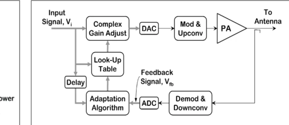
A block diagram of an adaptive digital predistortion system is shown in Figure 3. With the inclusion of DP, the digital complex baseband input signal samples are multi-plied before the DAC by complex coefficients drawn from the Look-Up-Table (LUT). The LUT coefficients imple-ment the predistortion function. The Adaptation Algorithm determines the values of the coefficients by comparing the feedback signal and a delayed version of the input signal. The complex gain adjuster and LUT blocks of Figure 3 are shown in more detail in Figure 4. The predistortion function is implemented using a com-plex multiplier, a LUT, and an Address Generation block that selects the appropriate coefficient from the LUT, given the magnitude of the input signal.
The size of the LUT employed determines the number of points at which the predistortion function is calculated. In addition, it is not necessary that the predistortion function points be evenly distributed across the range of the input signal magnitude. In some applications, it may be desirable to distribute the predistortion function points across the range of the input signal magnitude using a squared (power) or logarithmic relationship to provide a higher density of coefficients at the higher input power levels where the PA is most nonlinear [3, 4].
The function of the adaptation algorithm is to derive the predistortion function,F, in other words, the inverse
Figure 2 · Power amplifier Poutversus Pinand digital predistortion.
Figure 3 · Digital predistortion block diagram.
characteristic of the amplifier response. The predistortion function may be derived using either a modulated signal input (random signal) or a known training signal. The adaptation algorithm and its implementation are funda-mentally different depending upon which type of input signal is utilized. The algorithms that are based on the use of a modulated signal employ statistical signal pro-cessing and typically require some type of curve fitting algorithm to generate a smooth predistortion function. The complexity of the adaptation algorithm and its imple-mentation can be significantly simplified by using an alternative input signal—a known training signal [5].
The adaptation algorithm chosen for our implementa-tion is based on the use of a training signal. The training signal is a single tone having a frequency equal to the carrier frequency and whose power is ramped up during the training period. The power of the tone is set to zero at the start of the training period and will typically peak at, or just below, the maximum correctable input power of the amplifier.
Using a single tone whose power is ramped as a train-ing signal greatly simplifies the adaptation algorithm and its implementation. However, using the training signal requires interrupting the modulated signal while the training signal is transmitted. In addition, because the training signal is a single tone, the digital predistorter
only corrects for the operation of the amplifier at a single frequency, and not across the entire transmission band-width. If the amplifier’s passband is quite flat, using a single-tone training signal enables the predistortion func-tion to be determined accurately. Be aware, however, that using a single complex coefficient to correct for distortion of the amplifier at a particular power level presupposes minimal amplifier memory effects.
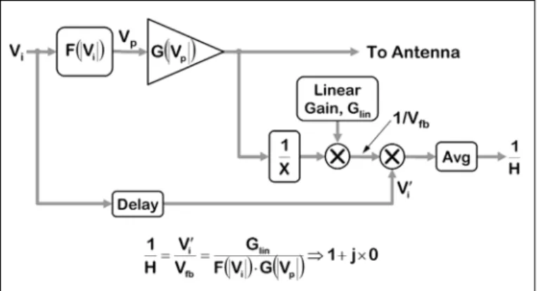
Figure 5 shows a block diagram of the adaptation algo-rithm. This algorithm is based on the determination of the open loop gain H of the predistorter and amplifier combination, at the power level associated with each LUT entry. Recall that the desired linear response of the pre-distorter and amplifier cascade requires that F(|Vi|) G(|Vp|) = kfor all inputs. Hence, if Glinis set to be equal to k, the desired open loop gain of the system is unity. If the calculated open loop gain is not equal to unity, the predistortion function must be adjusted to drive the open loop towards unity. Figure 6 illustrates this.
The predistortion function is defined by a set of coeffi-cients stored in the LUT,Ln, where each ncorresponds to an input signal magnitude that is mapped to a LUT address. To drive the open loop gain to unity, the predis-tortion function’s coefficients are updated by dividing each coefficient by the calculated open loop gain.
The delay in the feedback path is estimated by calcu-lating the correlation between the magnitude of the input signal and the magnitude of the feedback signal. The ben-efit of using the signal magnitude is that it does not require phase synchronization in the feedback path. Because the delay in the feedback path will not necessar-ily be equal to an integer number of DSP sample periods, interpolation is employed. The correlation between the input and feedback signal is performed on a modulated signal that precedes the training signal because the gain compression of the amplifier potentially degrades the accuracy of the correlator's estimation process during the training signal. In general, the accuracy of the estimation improves as the block size increases. However, a larger block size requires more memory and takes longer to cal-culate.
The predistortion function cannot be determined exactly by following the transmission of a single training ramp. It requires an iterative calculation of the LUT coef-ficients. A series of training ramps must be transmitted, although significant improvement to the amplifier Adjacent Channel Power Ratio (ACPR) is often observed following just two or three training ramps.
Connected Test Hardware-EDA Software Solution
The traditional design process for modern communica-tion systems typically uses Electronic Design Automacommunica-tion (EDA) tools (software) to create the first design using func-tional blocks and models. This is followed by intensive
sim-Figure 5 · Implementation of the adaptation algorithm.
24 High Frequency Electronics High Frequency Design
AMPLIFIER LINEARIZATION
ulation to understand the behavior of the design. Modifications are made until acceptable performance is achieved. Finally, a prototype is fabri-cated and evaluated with test and
measurement hardware. During this hardware measurement process, unexpected problems can arise due to model imperfections and simulation variables.
With our method, we combine EDA software with the test and mea-surement equipment to help meet emerging requirements that are not addressed by design software or instruments alone. In general, adding real measurements to a simulation helps ensure a successful prediction of the final performance.
Our method used the Advanced Design System (ADS, from Agilent Technologies) for EDA design and simulation. We also used the Linearization DesignGuide, which provides a complete tool kit to inter-actively explore dynamic lineariza-tion systems at the top level as part of an integrated design process. We connected these EDA software tools with test and measurement equip-ment (signal generator, signal source, and signal generator, also from Agilent Technologies) to create a con-nected software-hardware digital predistortion system. The system allowed us to work with realistic, complex, and customized test signals and measurements to gain added insight about the performance of the device-under-test.
Simulation and Measurement Results
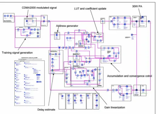
A 30 Wrms power amplifier was designed in ADS using a 170 W Motorola Laterally Diffused Metal Oxide Semiconductor or LDMOS device (MRF 9180) and simulated with the adaptive digital predistor-tion system in the 880 MHz band. Figure 7 illustrates the PA block dia-gram as defined in ADS. The PA con-sists of 3 stages: 1) a MRF9045 amplifier that has a drive amplifier (MHL9236), 2) a MRF9045 amplifier, and 3) a balanced MRF9180 amplifi-er. The PA, as designed, has 49 dB gain and 54 dBm saturated power. Figure 8 shows the entire ADS schematic of the digital predistorter wherein all subsystems have been implemented in the ADS Agilent Ptolemy simulation environment. Figure 9 illustrates the simulation
Figure 7 · The PA block diagram defined in ADS.
Figure 8 · The complete simulation schematic of the digital predistortion linearizer.
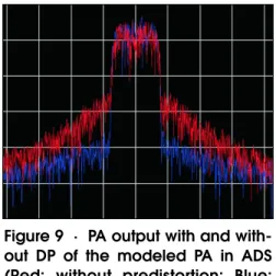
results. Approximately 20 dB of dis-tortion correction is achieved at the 45 W output power level.
Figure 10 illustrates the setup for interconnecting the Electronic Signal Generator (Agilent ESG E4438C), amplifier under test (DUT), Vector Signal Analyzer (Agilent VSA 89641A) and the ADS digital predis-torter system design. The DUT is illustrated in Figure 11.
The overall simulation of the pre-distorter consists of two separate ADS simulations—the ESG simula-tion and the VSA simulasimula-tion.
The ESG simulation generates and predistorts a modulated signal conforming the desired wireless stan-dard, passing it on to the ESG where the signal is modulated onto an RF carrier. Data files containing both the ideal signal and the predistorted sig-nal are also saved. The RF output of the ESG is directed to the power amplifier whose output is connected through an appropriate attenuator to the VSA. When the VSA simulation is run, the VSA instrument captures the received and downconverted sig-nal, then transfers the signal into the ADS environment. ADS then per-forms the signal processing necessary to align the received signal with the saved reference signals and adaptive-ly calculate and update the LUT coef-ficients. A CDMA2000 forward-link-modulated signal with a chip rate of
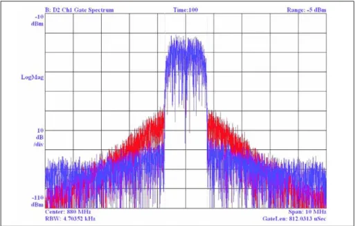
Figure 12 shows the PA output with digital predistortion. The power lev-els shown include attenuation to pro-tect the VSA’s input circuitry. Following three iterations at 45 watts of output power, the out-of-band spec-tra were reduced by over 15 dB.
due to factors such as temperature-based memory effects, test equipment bandwidth limitations (in this case the particular VSA used provided 39 MHz of bandwidth), and the inherent accuracy of the particular MOSFET device model used in ADS.
Figure 9 · PA output with and with-out DP of the modeled PA in ADS (Red: without predistortion; Blue: with predistortion).
High Frequency Design
AMPLIFIER LINEARIZATION
Conclusions
The adaptive digital predistortion system was imple-mented using the Advanced Design System EDA software package with the Linearization DesignGuide, connected to test equipment (ESG signal source and VSA signal analyzer). Through the use of a training signal, a simple adaptive algorithm was employed to update the LUT coef-ficients used to linearize a candidate Power Amplifier. Significant reduction in out-of-band distortion products was observed. The connected test hardware-EDA soft-ware solution approach can also provide key information to design engineers for optimizing the DSP architecture of a candidate PA linearized using digital predistortion. For example, the effect of changing the number of LUT coefficients may be rapidly observed. Further improve-ments may be possible by addressing other issues, such as temperature and electrical memory effects, as well as by using wider measurement bandwidths.
References
1. O. Ichiyoshi, “High-Power Linear Amplification Using Periodically Updated Amplitude and Phase Correction Values,” U.S. Patent No. 5,699,383, December 16, 1997.
2. F. Zavosh, et al., “Digital Predistortion Techniques for RF Power Amplifiers with CDMA Applications,” Microwave Journal, October 1999.
3. Intersil Application Note, Adaptive Predistortion Using the ISL5239, AN1028, September 2002.
4. K.J. Muhonen, M. Kavehrad and R.
Krishnamoorthy, “Look-up Table Techniques for Adaptive Digital Predistortion: A Development and Comparison,” IEEE Transactions on Vehicular Technology, vol. 49, no. 5, September 2000, pp. 1995-2002.
5. J. de Mingo and A. Valdovinos, “Performance of a New Digital Baseband Predistorter Using Calibration
Figure 10 · ESG, VSA, and PC hardware set-up in the connected solution.
Memory,” IEEE Transactions on Vehicular Technology, vol. 50, no. 4, July 2001, pp. 1169-1176.
Author Information
The authors include: Kelly Mekechuk, Wan-Jong Kim and Shawn P. Stapleton of the Mobile/RF Communications Laboratory, School of Engineering Science, Simon Fraser University, 8888 University Drive, Burnaby, BC V5A 1S6 Canada; and Jong Heon Kim of the Software Radio System Laboratory, Radio Science & Engineering, Kwangwoon University, 447-1, Wolgye, Nowon, Seoul 139-701 Korea.
employed as CTO at PropheSi Technologies. His research at SFU has focused on integrated RF/DSP applications for wireless communica-tions, GaAs MMIC circuits and PA and optical linearization. He received his BEng in 1982, MEng in 1984 and PhD in 1988 from Carleton University, Canada. Before joining Simon Fraser University, Shawn worked on a wide variety of projects including optical communications, RF/Microwave communications sys-tems, and adaptive array antennas. While at Simon Fraser University he developed a number of adaptive lin-earization techniques ranging from feedforward, active biasing and work function predistortion to digital base-band predistorters. He has developed PLL, linearization and communica-tions design software for the wireless industry. Earlier in his career, he was a Staff Scientist at Scientific Atlanta where he worked on CATV headend equipment.
Interested readers may contact Wan-Jong Kim ([email protected]) or Dr. Shawn Stapleton (sstapleton@ prophesitech.com
Figure 12 · PA output with and without DP of the actual hardware PA (Red: without predistortion, Blue: with predistortion).
Figure 11 · The 30 Wrms power amplifier developed for the lin-earization experiments.