Measuring Handler CDM Stress Provides Guidance for
Factory Static Controls
Arnold Steinman (1) and Timothy J. Maloney (2)
(1) Electronics Workshop/Dangelmayer Associates, 1321 Walnut Street, Berkeley, CA 94709 USA tel.: 510-549-3775, e-mail: [email protected]
(2) Intel Corporation, 2200 Mission College Blvd., SC9-09, Santa Clara, CA 95054 USA
Abstract - A handler simulator with a 50-ohm current detector creates CDM events for analysis and circuit
modeling. The 50 ohms is mathematically removed to leave only air spark resistance, and the synthesized waveform, with higher peak current, is shown to relate to both CDM tester results and E-field in the factory.
I. Introduction
Modern manufacturing increasingly depends on automated handlers to move components through processing steps. It has become important to characterize the capability of this equipment to handle components of a known Charged Device Model (CDM) ESD sensitivity, to avoid ESD damage to sensitive components. Beyond the equipment, it has also become important to be able to characterize an entire manufacturing process as to its capability to handle devices of known CDM ESD sensitivity. The question to be answered is simply, “can this equipment or process safely handle devices of a known ESD sensitivity.” The challenge is to develop test methods capable of answering this question.
Previous studies of CDM ESD in factory equipment [1,2] have shown how discharge currents in component handlers correlate with the currents in standardized CDM testers. In addition, these studies made a direct connection between the voltages producing the currents in the CDM testers and the voltages measured directly on devices with a high impedance contacting digital voltmeter (HIDVM).
The component handler simulator or discharge test fixture of [2] allows a component to be charged at some distance from the ground plane, and then discharged through a 50-ohm oscilloscope channel for easy detection. These CDM events are simple and easily-observed pulses, made all the more observable by the 50 ohms added to the air spark resistance, usually tens of ohms [3, 4]. Voltages on the device pins prior to discharge were verified by the HIDVM. Similar HIDVM measurements could be made on
devices prior to contact with grounded surfaces in actual manufacturing environments.
The primary reasons for using 50 ohms in the handler discharge test fixture are to produce higher amplitude, easily measured waveforms and the cost of specialized discharge resistors, such as those used in typical CDM testers. In the CDM Tester, the device discharges through a 1-ohm resistor. We would like to know what a handler CDM pulse would look like with this resistance so that we could compare the discharge in the handler to the discharge in the CDM tester more directly. Fortunately, the 50 ohms can be removed mathematically if we use the RLC approximation to the CDM waveform as was recently proposed [4]. The result is a waveform with the same total charge but a higher peak current and less damping.
From this waveform, the relationships connecting charge and peak current can be examined. These relationships directly correspond to voltage measurements made with the HIDVM and to the voltages used in CDM testers. It is also possible to calculate the E-field resulting from surface charge density on the device (related to device area).
damage. Correlation to HIDVM measurements and E-field measurements would be available as well. This work will describe the above topics for some component examples.
II. Discharge Fixture Waveforms
The discharge fixture, described in [2], operates like a handler as it holds a component by vacuum, allows the component to be pre-charged at a fixed height above the ground plane (2.5 mm), and then causes the part to contact the ground strip (0.125”x1.0”) on the target plane. This is schematically shown in Figure 1. A picture of the apparatus is shown in Figure 2.
Figure 1. The device creates mirror charge, then touches the pedestal and sends a pulse to the oscilloscope.
Figure 2. Discharge Test fixture
The oscilloscope detects the discharge and displays a waveform such as that shown in Figure 3, which results from discharging a 64-pin LQFP device. When a digital waveform is captured, we have a record suitable for applying the methods of [4] and simply extracting an approximate RLC network. The method uses peak current Ipk, first peak charge Qfp,
and total charge Qa, plus a charging voltage V0, to
formulate an RLC model matching the measured quantities exactly. The flow of the calculation is shown in Figure 4, taken from [4]. Total capacitance
C0 is found from C0V0=Qa, but equivalent resistance
and inductance Req and Leq are deduced from an
intermediate calculation of damping factor D, which relates to other quantities through transcendental equations described in [4].
Figure 3. Test fixture discharge for 500V, 64-pin device.
Qa
Qfp
Vo
Imax
Co
Leq D
Cmax
Req
derived quantity measured quantity
LC RC D
2 =
Figure 4. Flow of RLC calculation for the usual case of D<1, with Req, Leq and Co the series RLC parameters of an equivalent network.
We take the discrete points in Figure 3 (data provided by the oscilloscope) and plot them with smooth connections, and also fit them to an RLC discharge waveform, as shown in the curves of Figure 5a. The final choice of an RLC model depends on estimating how much voltage the device loses by the time it hits the ground plane, having been charged at a set height (2.5 mm for this work) above the ground plane. This voltage reduction factor f (taken to be 1.5 here) also multiplies the capacitance. Thus, initial charging of the device C0V0=Qa is solved for placement of the
device at 2.5 mm and then C=fC0 is the final
capacitance, discharged when the voltage has dropped to V=V0/f.
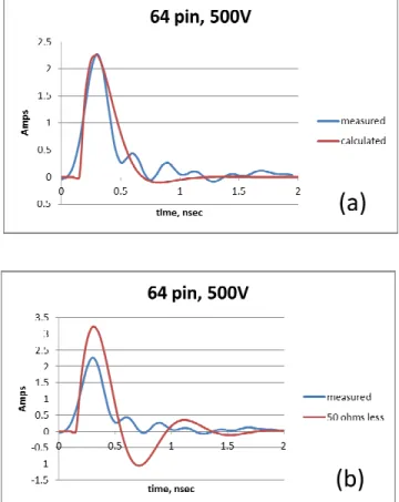
In the case of Figure 5a, the RLC values are as shown in Table 1c for the 64-pin device. Resistance R includes the 50 ohm scope impedance, so we subtract 50 ohms to leave the air spark resistance R0 and leave
step source V then approximates the discharge of the device into a pure ground plane, as shown in Figure 5b, with peak current about 1.5x higher than measured. Figure 6 shows the same kind of analysis for a 240-pin MQFP device, where the initial fit had damping factor D>1 and was more suitable for a centroid fit [4,5]. Again, voltage reduction factor f=1.5 was used. Measurement and modeling results at 50V, 250V, and 500V are summarized in Tables 1.
Figure 5. (a) 64-pin device waveform and RLC fit with 1.5x voltage reduction to 333.3V. (b) Same measured waveform compared with RLC fit having 50 ohms less resistance.
Figure 6. (a) 240-pin MQFP device waveform and RLC fit with 1.5x voltage reduction to 333.3V. (b) Same measured waveform compared with RLC fit having 50 ohms less resistance.
Table 1a. 50V charge, 2.5 mm
Quantity 64-pin LQFP 240-pin MQFP Vdischarge (V) 36 29.6
L (nH) 4.6 6
C (pF) 1.88 6.327
R (Ω) 159 193
R0 = R-50Ω 109 143
Qa (nC) 0.0677 0.187
Ipk(meas) (A) 0.189 0.142
Ipk (at R0) (A) 0.25 0.185
Ipk ratio 1.32 1.30
Table 1b. 250V charge, 2.5 mm
Quantity 64-pin LQFP 240-pin MQFP Vdischarge (V) 220 166.7
L (nH) 6 6.5
C (pF) 1.73 6.93
R (Ω) 226 185
R0 = R-50Ω 176 135
Qa (nC) 0.38 1.155
Ipk(meas) (A) 0.842 0.834
Ipk (at R0) (A) 1.03 1.097
Table 1c. 500V charge, 2.5 mm
Quantity 64-pin LQFP 240-pin MQFP Vdischarge(V) 333.3 333.3
L (nH) 8.09 6.83 C (pF) 1.81 7.87
R (Ω) 94.6 89
R0 = R-50Ω 44.6 39
Qa (nC) 0.603 2.62
Ipk(meas) (A) 2.27 3.09
Ipk (at R0) (A) 3.4 5.35
Ipk ratio 1.498 1.73
III.
Further Results and Discussion
1. All Peak Currents
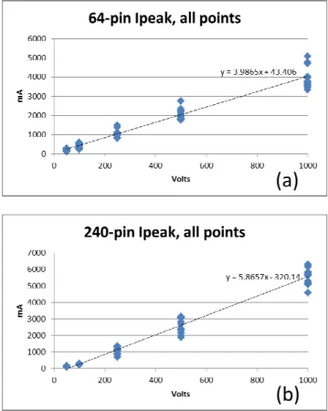
The results shown in Figs. 5-6 and Tables 1 are typical for an entire range of voltages applied to various samples of the two components. This is shown in Figure 7, where all Ipk results at all voltages were
plotted for the two components and linear regression lines computed. Tables 1 show that only at 500V does the larger 240-pin part have substantially more milliamps of peak current per discharge volt in a CDM pulse. At lower charging voltage (50, 250V) we have to guess at voltage reduction factor, and also find substantially higher equivalent spark resistance.
The intercept of the regression line for the 64-pin part is fairly close to zero, but for the 240-pin part it looks as if there could be arc extinction around 50V, which is not uncommon. But as we know, there is some voltage loss as the part approaches the ground plane, so the indicated “50V” should also have reduction factor f. For both parts, peak current has a basic linear relation to voltage, as expected.
2. Rise Times
The two-pole RLC approximations to the waveform are guaranteed to fit Qa, Qfp and Ipk [4], but rise time
matching may not happen without extra “rise time poles” as part of the model. This appears to be the case in Figures 5 and 6, and is also shown rather starkly in Figure 8, a 250V result for the large part. We think several things could be happening. These measurements were taken on a 3 GHz LeCroy oscilloscope (see Fig. 2) with 50 psec minimum time step, so the fastest rise times will be blurred a bit by the instrument. Aside from that, the air spark should have its own rise time poles to represent its finite
effective rise time, or perhaps even better, the resistance is really a time-dependent resistance (R[t]) coming down to a finite value from infinity, as discussed in the plasma physics picture of the air spark [6]. There is also some discussion of air spark R[t] in [4]. In any case, the observed rise times are explainable and do not affect our basic results.
Figure 7. (a) 64-pin LQFP peak currents, 12 devices, charging voltages at 2.5 mm. (b) Same situation for 240-pin MQFP.
3. Discharge Fixture Related to the CDM Tester
The handler test fixture of [2] plus its associated data, take us a step closer to relating CDM test results to measured factory conditions. Once the artificial 50 ohms is removed and the waveform recomputed, the handler test fixture results provide a link between total charge Qa and peak CDM current for a given part,
examples of which are seen in Table 1 for 500V.
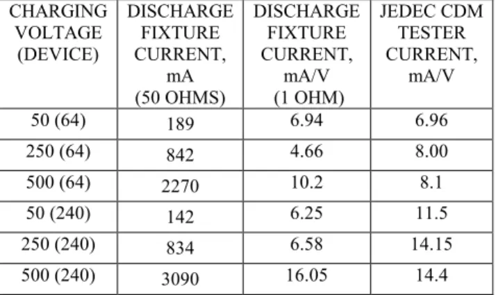
Discharge currents in the JEDEC CDM tester can then be compared those of the handler test fixture in the context of equipment CDM ESD handling capability. This is illustrated in Table 2. The data taken at 50-500 volts have to be adjusted for voltage reduction, as estimated in the first row of each of Tables 1. The second column of Table 2 lists peak current data from Tables 1. The third and fourth columns of Table 2 compare peak current per volt of discharge voltages from the handler fixture minus 50 ohms (column 3) and the CDM tester (column 4). Given that we had to estimate voltage reduction in the handler fixture and measure at a manifestly lower spark voltage, the comparisons are often remarkably good. The JEDEC CDM Ipk is usually more conservative, i.e., higher
than expected from the discharge fixture.
Table 2 – Comparison of discharge fixture and JEDEC CDM tester currents, typical examples
CHARGING VOLTAGE (DEVICE) DISCHARGE FIXTURE CURRENT, mA (50 OHMS) DISCHARGE FIXTURE CURRENT, mA/V (1 OHM) JEDEC CDM TESTER CURRENT, mA/V
50 (64) 189 6.94 6.96
250 (64) 842 4.66 8.00
500 (64) 2270 10.2 8.1
50 (240) 142 6.25 11.5
250 (240) 834 6.58 14.15
500 (240) 3090 16.05 14.4
Since we are able to make voltage measurements on devices in the factory with the HIDVM, we can directly correlate these measurements to the voltages in the CDM tester. This gives us a quantitative method of making a factory measurement to establish equipment and process capability to handle ESD-sensitive devices.
IV.
Relation to E-Fields
If we now consider that the total charge must be spread across the surface area Ad of the device (or 2Ad
for both sides of the device), this allows calculation of the E-field emerging from such a charged device. This would relate to factory measurements that could be made with a field meter, showing what sort of charge can be induced on the devices or measured on devices already charged. The E-field is computed through Gauss’ Law from the deduced amount of surface charge:
)
/
(
)
(
2
)
(
)
/
(
0 2cm
pF
cm
A
pC
Q
cm
V
E
d aε
=
, (1)where ε0=0.08854 pF/cm and the factor of 2 shows the minimum field that can be produced by a flat device with cross-sectional area Ad—the 2-sided
worst case, where often a case of induced charge from another object will be 1-sided. The same might be true of devices charged triboelectrically when only one side of the device is contacted during the handling process.
The field estimate can thus be related to field meter measurements from the factory. For example, a baseline E-field outdoors in clear weather is typically 100V/m or 1V/cm, which can be detected with a field mill [7], but measurements below that are unlikely. From (1), this corresponds to 88.54 fC/cm2 of total surface area. Typical desired factory limits are more like 200V/inch, or about 80V/cm, corresponding to 7.08 pC/cm2. This gives us a feel for how much charge could appear on the parts for a given E-field, and from there we can work toward values of possible Ipk and compare with CDM tester data.
Table 3—Relating peak current to E-field
Quantity 64-pin LQFP
240-pin MQFP
Ad (cm2) 1.44 12.15
Ipk/Qa (GHz) 5.64 2.04
Ipk/E (kV/cm) 1.44 4.39
CDM test voltage (1kV/cm 2-sided
E-field)
200-225V 250-300V
Table 3 shows quantities for our 64-pin and 240-pin parts derived from Table 1 and from [2], converging on a field-related figure of merit (FOM) for Ipk as
that the effective device capacitance for the CDM tester is higher than it is for the handler discharge test fixture, so the charge quantities Qa in the CDM tester
are guaranteed to be sufficient.
The results of Table 1c were used to find an approximate CDM test voltage (last row of Table 3) that produces the Ipk corresponding to an E-field
(2-sided) of 1kV/cm. Recall that 1kV/cm is a factor of 12.5x more than the 200V/inch E-field goal, plus the additional 2x worst-case factor as noted above. The 200V/inch goal would provide a significant safety factor for determining product handling capability in the 200-300 volt range.
While E-field measurements do not pick up all cases of device charging, these studies show that present-day CDM test goals around 250V are quite compatible with static control goals. Product loss due to CDM in the factory is likely to be explained by unusually weak parts or by unusual static charging events. One well-known example of the latter would be a huge collection area for the E-field, one the size of a printed circuit board instead of a small component (charged board event, or CBE). Avoidance of discharge events becomes a priority in such a case. Future work might examine the relationship between measured E-field and the resulting CBE discharge currents.
V.
Conclusions
An analysis of CDM discharge results from a component handler discharge simulator described previously [2] has been able to mathematically remove the 50 ohms of the oscilloscope channel detector. The waveforms from sets of two different size components were approximated by RLC models [4] and transformed to waveforms with 50 ohms less resistance, leaving only the air spark resistance and equivalent inductance and capacitance of the discharge environment. Higher peak currents resulted, as expected, and the waveforms became closer to their counterparts on the JEDEC/ESDA CDM tester, yet more precisely describe a component handler discharge. With the ability to precisely measure the actual voltage induced on a device at a given point in the manufacturing process, we have a method for describing equipment or process ESD handling capability.
The equivalent air spark resistance increases for lower discharge voltage, so Ipk will be weaker than expected
if scaled down to 50-100V from the 250-500V level.
This agrees with air spark data as reported in 2010 for the CDM tester [8], which showed that a 50-ohm relay-based CDM2 test could agree with low voltage (~100V) CDM Ipk, while air spark Ipk has much
variation. At higher voltages (250-500V), a 25-ohm relay-based CDM2 test [4] should match CDM air spark Ipk more closely.
With charge (Qa) data also joining the Ipk data, we
describe for these components a relation between worst-case CDM peak current and environmental E-fields as customarily measured in the manufacturing environment. These results can also then be mapped back to pre-existing data from the standard CDM tester, in order to find the true resilience of a given component during its handling in equipment or a manufacturing process.
VI. References
[1] A. Steinman, L.G. Henry, and M. Hernandez, “Measurements to Establish Process ESD
Compatibility,” in Proc. EOS/ESD Symposium, 2010, pp. 225-232. [Online]. Available:
http://ieeexplore.ieee.org/stamp/stamp.jsp?tp=&arnu mber=5623733.
[2] A. Steinman, “Equipment ESD Capability
Measurements”, in Proc. EOS/ESD Symposium, 2013, pp. 48-55. [Online]. Available:
http://ieeexplore.ieee.org/stamp/stamp.jsp?tp=&arnu mber=6635904
[3] B.C. Atwood, Y. Zhou, D. Clarke, and T. Weyl, “Effect of Large Device Capacitance on FICDM Peak Current,” in Proc. EOS/ESD Symposium, 2007, pp. 273-282. [Online]. Available:
http://ieeexplore.ieee.org/stamp/stamp.jsp?tp=&arnu mber=4401763.
[4] T.J. Maloney and N. Jack, “CDM Tester Properties as Deduced from Waveforms,” in Proc. EOS/ESD Symposium, 2013, pp. 374-382. [Online]. Available:
http://ieeexplore.ieee.org/stamp/stamp.jsp?tp=&arnu mber=6635950. Expanded version is in IEEE Trans. Mat. Dev. Reliability, 2014 (to be published). [Online]. Available:
[5] T.J. Maloney, "HBM Tester Waveforms, Equivalent Circuits, and Socket Capacitance," in Proc. EOS/ESD Symposium, 2010, pp. 407-415. [Online]. Available:
http://ieeexplore.ieee.org/stamp/stamp.jsp?tp=&arnu mber=5623761. Slightly revised version in
Microelectronics Reliability, vol. 53, pp. 184–189 (2013).
[6] R.G. Renninger, "Mechanisms of Charged-Device Electrostatic Discharges," in Proc. EOS/ESD
Symposium, 1991, pp. 127-143.
[7] [Online]. Available:
http://a-tech.net/ElectricFieldMill/
[8] R. Given, M. Hernandez, and T. Meuse, “CDM2—A New CDM Test Method for Improved Test Repeatability and Reproducibility,” in Proc. EOS/ESD Symposium, 2010, pp. 359-367. [Online]. Available: