Available
HIGH VOLTAGE TEMPERATURE
COMPENSATED ZENER REFERENCE DIODES
Screening in
reference to
MIL-PRF-19500
available
DESCRIPTION
The 1N4057 through 1N4085A series of temperature compensated reference diodes provides
a wide selection of nominal voltages ranging from 12.4 V to 200 V with low temperature
coefficients of either 0.005%/C or 0.002%/
oC for minimal voltage change with temperature.
This is achieved at the specified test currents of:
- 10.0 mA for the lower voltages 12.4 V to 33 V
- 7.5 mA for the next higher voltage grouping of 37 V to 100 V
- 5.00 mA for 68 V to 100 V
- 2.5 mA for the highest voltage group 105 V to 200 V
These axial-leaded reference diodes are packaged in three different plastic body package
configurations progressively increasing in size with the voltage. Microsemi also offers
numerous other Zener reference diode products in smaller packages for lower voltages in
popular JEDEC registrations.
Packaging
Important: For the latest information, visit our website
http://www.microsemi.com
.
FEATURES
•
JEDEC registered 1N4057 thru 1N4085.
•
Hermetically sealed, metallurgically bonded, double-plug construction.
•
Standard voltage tolerances of +/- 5 %.
•
Maximum temperature coefficient selections available of 0.005 %/
oC and 0.002 %/
oC.
•
Up-screening available in reference to MIL-PRF-19500.
(See
part nomenclature
for all available options.)
•
RoHS compliant versions available.
APPLICATIONS / BENEFITS
•
Provides minimal voltage change in voltage over a broad temperature range.
•
For instrumentation and other circuit designs requiring a stable voltage reference.
•
Flexible axial-lead mounting terminals.
•
Non-sensitive to ESD per MIL-STD-750 method 1020.
MAXIMUM RATINGS
MSC – Lawrence
6 Lake Street,
Lawrence, MA 01841
Tel: 1-800-446-1158 or
(978) 620-2600
Fax: (978) 689-0803
MSC – Ireland
Gort Road Business Park,
Ennis, Co. Clare, Ireland
Tel: +353 (0) 65 6840044
Fax: +353 (0) 65 6822298
Website:
www.microsemi.com
Parameters/Test Conditions
Symbol
Value
Unit
Junction and Storage Temperature
T
Jand T
STG-65 to +175
ºC
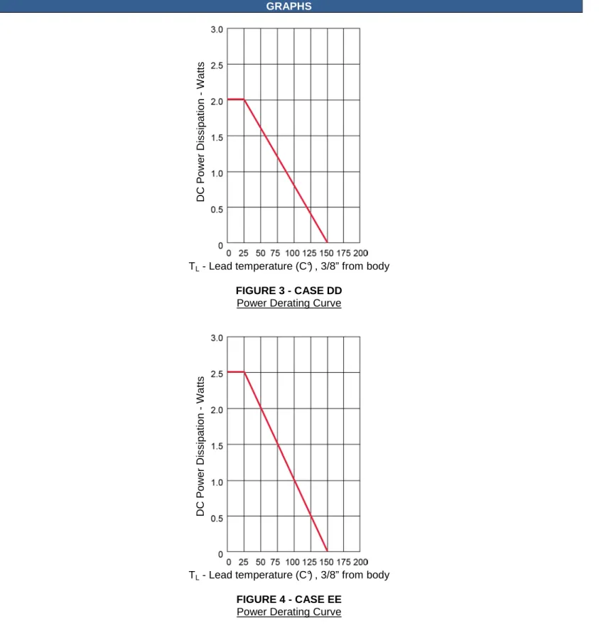
Off-State Power Dissipation
(1)Case CC
Case DD
Case EE
P
D1.5
2
2.5
W
Solder Temperature @ 10 s
T
SP260
oC
Notes: 1. Starting at 25 ºC, derate linearly to zero at 150 ºC:
Case CC derate at 12 mW/ºC
Case DD derate at 16 mW/ºC
Case EE derate at 20 mW/ºC
MECHANICAL and PACKAGING
•
CASE: Plastic shell filled with non-conductive epoxy around a hermetically sealed glass encased diode.
•
TERMINALS: Tin-lead or RoHS compliant matte-tin plated copper clad steel solderable per MIL-STD-750, method 2026.
•
MARKING: Part number and cathode band.
•
POLARITY: Reference diode to be operated with the banded end positive with respect to the opposite end.
•
TAPE & REEL option: Consult factory for quantities.
•
WEIGHT: Case CC: 1.17 grams
Case DD: 1.42 grams
Case EE: 2.86 grams
•
See
Package Dimensions
on last page.
PART NOMENCLATURE
JAN
1N4057
A
(e3)
Reliability Level
MQ (reference JAN)
MX (reference JANTX)
MV (reference JANTXV)
CDS (reference JANS)
Blank = Commercial
JEDEC type number
(See
Electrical Characteristics
table)
RoHS Compliance
e3 = RoHS compliant
Blank = non-RoHS compliant
Temperature Coefficient
A = +/- .002 % / ºC
Blank = +/- .005 % / ºC
SYMBOLS & DEFINITIONS
Symbol
Definition
I
Z, I
ZT, I
ZKRegulator Current: The dc regulator current (I
Z), at a specified test point (I
ZT), near breakdown knee (I
ZK).
P
DPower Dissipation: The power dissipation, dc.
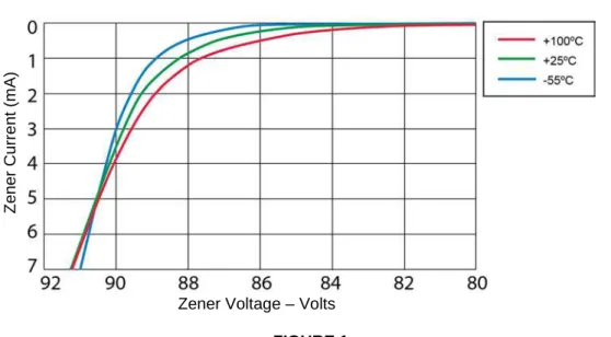
ELECTRICAL CHARACTERISTICS
JEDEC TYPE NUMBER ZENER VOLTAGE (See Note 1) VZ @ IZT ZENER TEST CURRENT IZT MAXIMUM DYNAMICS IMPEDANCE Zx @ IZT MAXIMUM TEMPERATURE COEFFICIENT (See Note 2)α
VZTEMPERATURE RANGE CASE TYPE NO. Volts (+/- 5%) mA Ohms +/ -% / o C +/- mV / o C o C 1N4057 1N4057A 12.4 12.4 10.0 10.0 25 25 .005 .002 .62 .25 55 to +25 to +100 55 to +25 to +100 CC CC 1N4058 1N4058A 14.6 14.6 10.0 10.0 30 30 .005 .002 .73 .29 55 to +25 to +100 55 to +25 to +100 CC CC 1N4059 1N4059A 16.8 16.8 10.0 10.0 30 30 .005 .002 .84 .34 55 to +25 to +100 55 to +25 to +100 CC CC 1N4060 1N4060A 18.5 18.5 10.0 10.0 30 30 .005 .002 .92 .37 55 to +25 to +100 55 to +25 to +100 CC CC 1N4061 1N4061A 21 21 10.0 10.0 35 35 .005 .002 1.05 .42 55 to +25 to +100 55 to +25 to +100 CC CC 1N4062 1N4062A 23 23 10.0 10.0 40 40 .005 .002 1.15 .46 55 to +25 to +100 55 to +25 to +100 CC CC 1N4063 1N4063A 27 27 10.0 10.0 45 45 .005 .002 1.35 .54 55 to +25 to +100 55 to +25 to +100 CC CC 1N4064 1N4064A 30 30 10.0 10.0 50 50 .005 .002 1.50 .60 55 to +25 to +100 55 to +25 to +100 CC CC 1N4065 1N4065A 33 33 10.0 10.0 55 55 .005 .002 1.65 .66 55 to +25 to +100 55 to +25 to +100 CC CC 1N4066 1N4066A 37 37 7.5 7.5 80 80 .005 .002 1.85 .74 55 to +25 to +100 55 to +25 to +100 CC CC 1N4067 1N4067A 43 43 7.5 7.5 90 90 .005 .002 2.15 .86 55 to +25 to +100 55 to +25 to +100 CC CC 1N4068 1N4068A 47 47 7.5 7.5 100 100 .005 .002 2.35 .94 55 to +25 to +100 55 to +25 to +100 CC CC 1N4069 1N4069A 51 51 7.5 7.5 110 110 .005 .002 2.55 1.02 55 to +25 to +100 55 to +25 to +100 DD DD 1N4070 1N4070A 56 56 7.5 7.5 120 120 .005 .002 2.80 1.12 55 to +25 to +100 55 to +25 to +100 DD DD 1N4071 1N4071A 62 62 7.5 7.5 135 135 .005 .002 3.10 1.24 55 to +25 to +100 55 to +25 to +100 DD DD 1N4072 1N4072A 68 68 5.0 5.0 230 230 .005 .002 3.40 1.36 55 to +25 to +100 55 to +25 to +100 DD DD 1N4073 1N4073A 75 75 5.0 5.0 250 250 .005 .002 3.75 1.50 55 to +25 to +100 55 to +25 to +100 DD DD 1N4074 1N4074A 82 82 5.0 5.0 270 270 .005 .002 4.10 1.64 55 to +25 to +100 55 to +25 to +100 DD DD 1N4075 1N4075A 87 87 5.0 5.0 290 290 .005 .002 4.35 1.74 55 to +25 to +100 55 to +25 to +100 DD DD 1N4076 1N4076A 91 91 5.0 5.0 310 310 .005 .002 4.55 1.82 55 to +25 to +100 55 to +25 to +100 DD DD 1N4077 1N4077A 100 100 5.0 5.0 340 340 .005 .002 5.00 2.00 55 to +25 to +100 55 to +25 to +100 DD DD 1N4078 1N4078A 105 105 2.5 2.5 700 700 .005 .002 5.25 2.10 55 to +25 to +100 55 to +25 to +100 DD DD 1N4079 1N4079A 110 110 2.5 2.5 740 740 .005 .002 5.50 2.20 55 to +25 to +100 55 to +25 to +100 DD DD 1N4080 1N4080A 120 120 2.5 2.5 800 800 .005 .002 6.00 2.40 55 to +25 to +100 55 to +25 to +100 DD DD 1N4081 1N4081A 130 130 2.5 2.5 840 840 .005 .002 6.50 2.60 55 to +25 to +100 55 to +25 to +100 EE EE 1N4082 1N4082A 140 140 2.5 2.5 960 960 .005 .002 7.00 2.80 55 to +25 to +100 55 to +25 to +100 EE EE 1N4083 1N4083A 150 150 2.5 2.5 1020 1020 .005 .002 7.50 3.00 55 to +25 to +100 55 to +25 to +100 EE EE 1N4084 1N4084A 175 175 2.5 2.5 1150 1150 .005 .002 8.75 3.50 55 to +25 to +100 55 to +25 to +100 EE EE 1N4085 1N4085A 200 200 2.5 2.5 1350 1350 .005 .002 10.00 4.00 55 to +25 to +100 55 to +25 to +100 EE EE
*JEDEC Registered Data